Äîêóìåíòàöèÿ è îïèñàíèÿ www.docs.chipfind.ru
SN74LVC2952A
OCTAL BUS TRANSCEIVER AND REGISTER
WITH 3-STATE OUTPUTS
SCAS311F JANUARY 1993 REVISED JUNE 1998
1
POST OFFICE BOX 655303
·
DALLAS, TEXAS 75265
D
EPIC
TM
(Enhanced-Performance Implanted
CMOS) Submicron Process
D
Typical V
OLP
(Output Ground Bounce)
< 0.8 V at V
CC
= 3.3 V, T
A
= 25
°
C
D
Typical V
OHV
(Output V
OH
Undershoot)
> 2 V at V
CC
= 3.3 V, T
A
= 25
°
C
D
Power Off Disables Outputs, Permitting
Live Insertion
D
Supports Mixed-Mode Signal Operation on
All Ports (5-V Input/Output Voltage With
3.3-V V
CC
)
D
ESD Protection Exceeds 2000 V Per
MIL-STD-883, Method 3015; Exceeds 200 V
Using Machine Model (C = 200 pF, R = 0)
D
Latch-Up Performance Exceeds 250 mA Per
JESD 17
D
Package Options Include Plastic
Small-Outline (DW), Shrink Small-Outline
(DB), and Thin Shrink Small-Outline (PW)
Packages
description
This octal bus transceiver and register is designed for 1.65-V to 3.6-V V
CC
operation.
The SN74LVC2952A consists of two 8-bit back-to-back registers that store data flowing in both directions
between two bidirectional buses. Data on the A or B bus is stored in the registers on the low-to-high transition
of the clock (CLKAB or CLKBA) input, provided that the clock-enable (CLKENAB or CLKENBA) input is low.
Taking the output-enable (OEAB or OEBA) input low accesses the data on either port.
Inputs can be driven from either 3.3-V or 5-V devices. This feature allows the use of these devices as translators
in a mixed 3.3-V/5-V system environment.
To ensure the high-impedance state during power up or power down, OE should be tied to V
CC
through a pullup
resistor; the minimum value of the resistor is determined by the current-sinking capability of the driver.
The SN74LVC2952A is characterized for operation from 40
°
C to 85
°
C.
Copyright
©
1998, Texas Instruments Incorporated
PRODUCTION DATA information is current as of publication date.
Products conform to specifications per the terms of Texas Instruments
standard warranty. Production processing does not necessarily include
testing of all parameters.
Please be aware that an important notice concerning availability, standard warranty, and use in critical applications of
Texas Instruments semiconductor products and disclaimers thereto appears at the end of this data sheet.
EPIC is a trademark of Texas Instruments Incorporated.
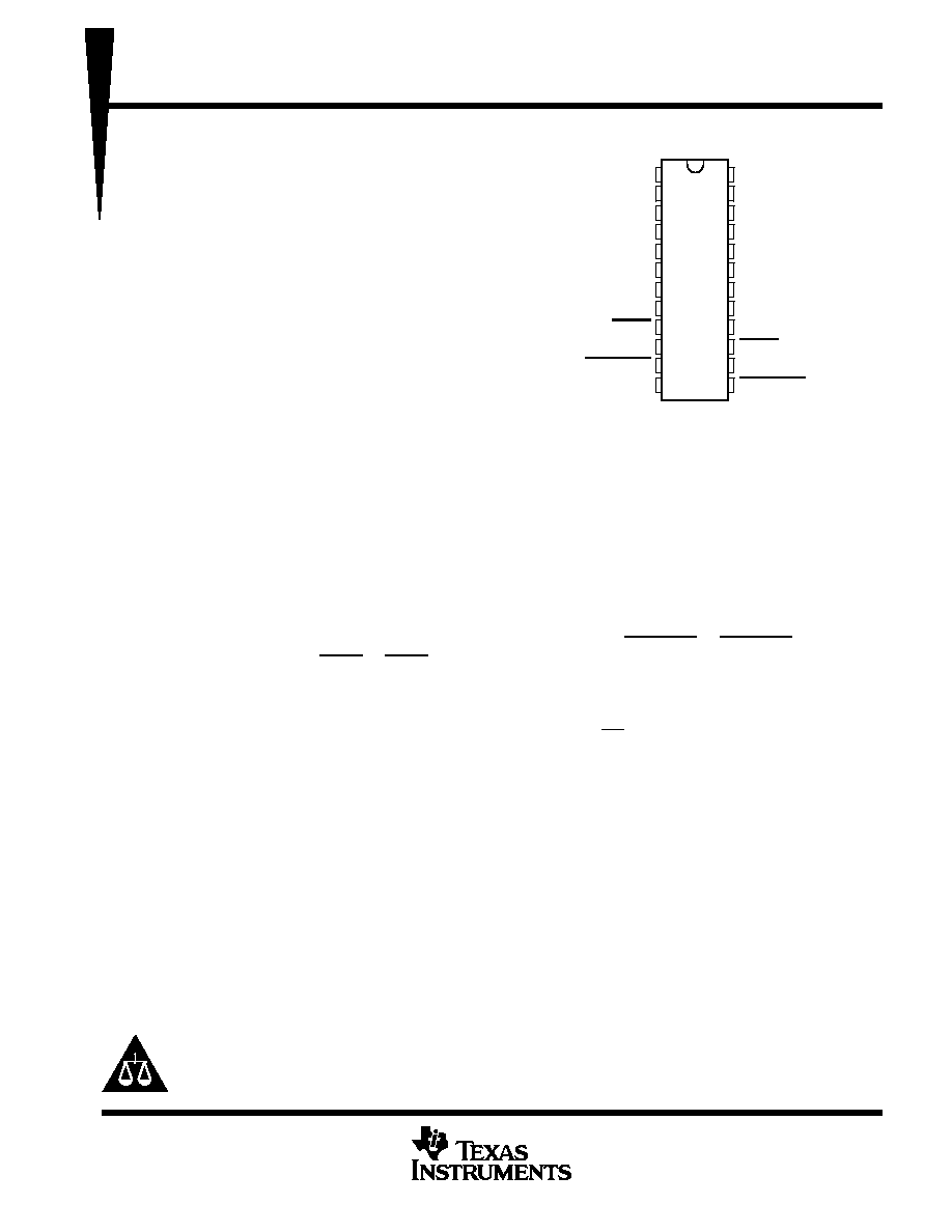
1
2
3
4
5
6
7
8
9
10
11
12
24
23
22
21
20
19
18
17
16
15
14
13
B8
B7
B6
B5
B4
B3
B2
B1
OEAB
CLKAB
CLKENAB
GND
V
CC
A8
A7
A6
A5
A4
A3
A2
A1
OEBA
CLKBA
CLKENBA
DB, DW, OR PW PACKAGE
(TOP VIEW)
SN74LVC2952A
OCTAL BUS TRANSCEIVER AND REGISTER
WITH 3-STATE OUTPUTS
SCAS311F JANUARY 1993 REVISED JUNE 1998
2
POST OFFICE BOX 655303
·
DALLAS, TEXAS 75265
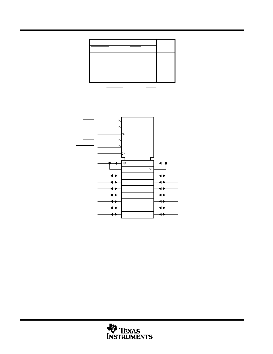
FUNCTION TABLE
INPUTS
OUTPUT
CLKENAB
CLKAB
OEAB
A
OUTPUT
B
H
X
L
X
B0
X
H or L
L
X
B0
L
L
L
L
L
L
H
H
X
X
H
X
Z
A-to-B data flow is shown; B-to-A data flow is similar,
but uses CLKENBA, CLKBA, and OEBA.
Level of B before the indicated steady-state input
conditions were established
logic symbol
§
B1
8
5D
A1
16
A2
17
A3
18
A4
19
EN3
15
1 C5
B2
7
B3
6
B4
5
A5
20
A6
21
A7
22
A8
23
B5
4
B6
3
B7
2
B8
1
G2
11
G1
13
EN4
9
2 C6
OEBA
CLKENBA
OEAB
CLKENAB
14
CLKBA
10
CLKAB
§ This symbol is in accordance with ANSI/IEEE Std 91-1984 and IEC Publication 617-12.
1
1
3
4
6D
SN74LVC2952A
OCTAL BUS TRANSCEIVER AND REGISTER
WITH 3-STATE OUTPUTS
SCAS311F JANUARY 1993 REVISED JUNE 1998
3
POST OFFICE BOX 655303
·
DALLAS, TEXAS 75265
logic diagram (positive logic)
To Seven Other Channels
B1
A1
OEBA
CLKBA
CLKENBA
OEAB
CLKAB
CLKENAB
8
C1
1D
C1
1D
11
10
9
13
14
15
16
SN74LVC2952A
OCTAL BUS TRANSCEIVER AND REGISTER
WITH 3-STATE OUTPUTS
SCAS311F JANUARY 1993 REVISED JUNE 1998
4
POST OFFICE BOX 655303
·
DALLAS, TEXAS 75265
absolute maximum ratings over operating free-air temperature range (unless otherwise noted)
Supply voltage range, V
CC
0.5 V to 6.5 V
. . . . . . . . . . . . . . . . . . . . . . . . . . . . . . . . . . . . . . . . . . . . . . . . . . . . . . . . .
Input voltage range, V
I
: (see Note 1)
0.5 V to 6.5 V
. . . . . . . . . . . . . . . . . . . . . . . . . . . . . . . . . . . . . . . . . . . . . . . .
Voltage range applied to any output in the high-impedance or power-off state, V
O
(see Note 1)
0.5 V to 6.5 V
. . . . . . . . . . . . . . . . . . . . . . . . . . . . . . . . . . . . . . . . . . . . . . . . . . . . . . . . . . . . . . . . . . .
Voltage range applied to any output in the high or low state, V
O
(see Notes 1 and 2)
0.5 V to V
CC
+ 0.5 V
. . . . . . . . . . . . . . . . . . . . . . . . . . . . . . . . . . . . . . . . . . . . . . . . . . . . . . .
Input clamp current, I
IK
(V
I
< 0)
50 mA
. . . . . . . . . . . . . . . . . . . . . . . . . . . . . . . . . . . . . . . . . . . . . . . . . . . . . . . . . . .
Output clamp current, I
OK
(V
O
< 0)
50 mA
. . . . . . . . . . . . . . . . . . . . . . . . . . . . . . . . . . . . . . . . . . . . . . . . . . . . . . . .
Continuous output current, I
O
±
50 mA
. . . . . . . . . . . . . . . . . . . . . . . . . . . . . . . . . . . . . . . . . . . . . . . . . . . . . . . . . . . . .
Continuous current through V
CC
or GND
±
100 mA
. . . . . . . . . . . . . . . . . . . . . . . . . . . . . . . . . . . . . . . . . . . . . . . . . .
Package thermal impedance,
JA
(see Note 3): DB package
104
°
C/W
. . . . . . . . . . . . . . . . . . . . . . . . . . . . . . . .
DW package
81
°
C/W
. . . . . . . . . . . . . . . . . . . . . . . . . . . . . . . . .
PW package
120
°
C/W
. . . . . . . . . . . . . . . . . . . . . . . . . . . . . . . .
Storage temperature range, T
stg
65
°
C to 150
°
C
. . . . . . . . . . . . . . . . . . . . . . . . . . . . . . . . . . . . . . . . . . . . . . . . . . .
Stresses beyond those listed under "absolute maximum ratings" may cause permanent damage to the device. These are stress ratings only, and
functional operation of the device at these or any other conditions beyond those indicated under "recommended operating conditions" is not
implied. Exposure to absolute-maximum-rated conditions for extended periods may affect device reliability.
NOTES:
1. The input negative-voltage and output voltage ratings may be exceeded if the input and output current ratings are observed.
2. The value of VCC is provided in the recommended oprating conditions table.
3. The package thermal impedance is calculated in accordance with JESD 51.
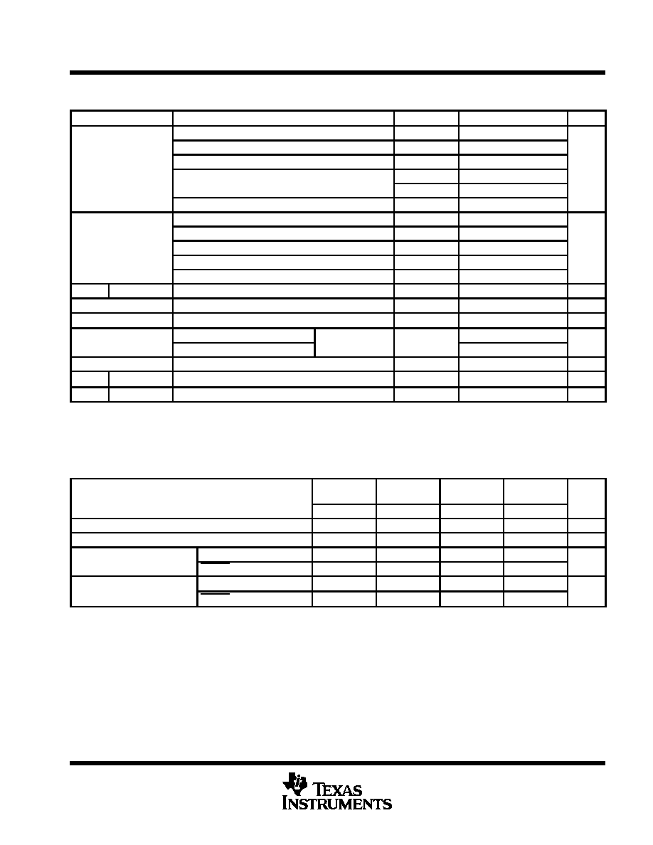
recommended operating conditions (see Note 4)
MIN
MAX
UNIT
VCC
Supply voltage
Operating
1.65
3.6
V
VCC
Supply voltage
Data retention only
1.5
V
VCC = 1.65 V to 1.95 V
0.65
×
VCC
VIH
High-level input voltage
VCC = 2.3 V to 2.7 V
1.7
V
VCC = 2.7 V to 3.6 V
2
VCC = 1.65 V to 1.95 V
0.35
×
VCC
VIL
Low-level input voltage
VCC = 2.3 V to 2.7 V
0.7
V
VCC = 2.7 V to 3.6 V
0.8
VI
Input voltage
0
5.5
V
VO
Output voltage
High or low state
0
VCC
V
VO
Output voltage
3 state
0
5.5
V
VCC = 1.65 V
4
IOH
High level output current
VCC = 2.3 V
8
mA
IOH
High-level output current
VCC = 2.7 V
12
mA
VCC = 3 V
24
VCC = 1.65 V
4
IOL
Low level output current
VCC = 2.3 V
8
mA
IOL
Low-level output current
VCC = 2.7 V
12
mA
VCC = 3 V
24
t/
v
Input transition rise or fall rate
0
10
ns/V
TA
Operating free-air temperature
40
85
°
C
NOTE 4: All unused inputs of the device must be held at VCC or GND to ensure proper device operation. Refer to the TI application report,
Implications of Slow or Floating CMOS Inputs, literature number SCBA004.
SN74LVC2952A
OCTAL BUS TRANSCEIVER AND REGISTER
WITH 3-STATE OUTPUTS
SCAS311F JANUARY 1993 REVISED JUNE 1998
5
POST OFFICE BOX 655303
·
DALLAS, TEXAS 75265
electrical characteristics over recommended operating free-air temperature range (unless
otherwise noted)
PARAMETER
TEST CONDITIONS
VCC
MIN
TYP
MAX
UNIT
IOH = 100
µ
A
1.65 V to 3.6 V
VCC0.2
IOH = 4 mA
1.65 V
1.2
VOH
IOH = 8 mA
2.3 V
1.7
V
VOH
IOH = 12 mA
2.7 V
2.2
V
IOH = 12 mA
3 V
2.4
IOH = 24 mA
3 V
2.2
IOL = 100
µ
A
1.65 V to 3.6 V
0.2
IOL = 4 mA
1.65 V
0.45
VOL
IOL = 8 mA
2.3 V
0.7
V
IOL = 12 mA
2.7 V
0.4
IOL = 24 mA
3 V
0.55
II
Control inputs
VI = 0 to 5.5 V
3.6 V
±
5
µ
A
Ioff
VI or VO = 5.5 V
0
±
10
µ
A
IOZ
VO = 0 to 5.5 V
3.6 V
±
10
µ
A
ICC
VI = VCC or GND
IO = 0
3 6 V
10
µ
A
ICC
3.6 V
VI
5.5 V§
IO = 0
3.6 V
10
µ
A
ICC
One input at VCC 0.6 V, Other inputs at VCC or GND
2.7 V to 3.6 V
500
µ
A
Ci
Control inputs
VI = VCC or GND
3.3 V
5
pF
Cio
A or B ports
VO = VCC or GND
3.3 V
8.5
pF
All typical values are at VCC = 3.3 V, TA = 25
°
C.
For I/O ports, the parameter IOZ includes the input leakage current.
§ This applies in the disabled state only.
timing requirements over recommended operating free-air temperature range (unless otherwise
noted) (see Figures 1 through 3)
VCC = 1.8 V
±
0.15 V
VCC = 2.5 V
±
0.2 V
VCC = 2.7 V
VCC = 3.3 V
±
0.3 V
UNIT
MIN
MAX
MIN
MAX
MIN
MAX
MIN
MAX
fclock
Clock frequency
¶
¶
150
150
MHz
tw
Pulse duration, CLK high or low
¶
¶
3.3
3.3
ns
t
Setup time
Data before CLK high
¶
¶
1.7
1.3
ns
tsu
Setup time
CLKEN before CLK high
¶
¶
1.3
1.1
ns
th
Hold time
Data after CLK high
¶
¶
1.8
1.1
ns
th
Hold time
CLKEN after CLK high
¶
¶
1.4
1.1
ns
¶ This information was not available at the time of publication.
SN74LVC2952A
OCTAL BUS TRANSCEIVER AND REGISTER
WITH 3-STATE OUTPUTS
SCAS311F JANUARY 1993 REVISED JUNE 1998
6
POST OFFICE BOX 655303
·
DALLAS, TEXAS 75265
switching characteristics over recommended operating free-air temperature range (unless
otherwise noted) (see Figures 1 through 3)
PARAMETER
FROM
(INPUT)
TO
(OUTPUT)
VCC = 1.8 V
±
0.15 V
VCC = 2.5 V
±
0.2 V
VCC = 2.7 V
VCC = 3.3 V
±
0.3 V
UNIT
(INPUT)
(OUTPUT)
MIN
MAX
MIN
MAX
MIN
MAX
MIN
MAX
fmax
150
150
MHz
tpd
CLKAB or CLKBA
B or A
8.8
1
8.2
ns
ten
OE
A or B
9
1
7.8
ns
tdis
OE
A or B
8.8
1
7.8
ns
tsk(o)
1
ns
This information was not available at the time of publication.
Skew between any two outputs of the same package switching in the same direction
operating characteristics, T
A
= 25
°
C
PARAMETER
TEST
CONDITIONS
VCC = 1.8 V
±
0.15 V
VCC = 2.5 V
±
0.2 V
VCC = 3.3 V
±
0.3 V
UNIT
CONDITIONS
TYP
TYP
TYP
Cpd
Power dissipation capacitance
Outputs enabled
f = 10 MHz
79
pF
Cpd
per transceiver
Outputs disabled
f = 10 MHz
41
pF
This information was not available at the time of publication.
SN74LVC2952A
OCTAL BUS TRANSCEIVER AND REGISTER
WITH 3-STATE OUTPUTS
SCAS311F JANUARY 1993 REVISED JUNE 1998
7
POST OFFICE BOX 655303
·
DALLAS, TEXAS 75265
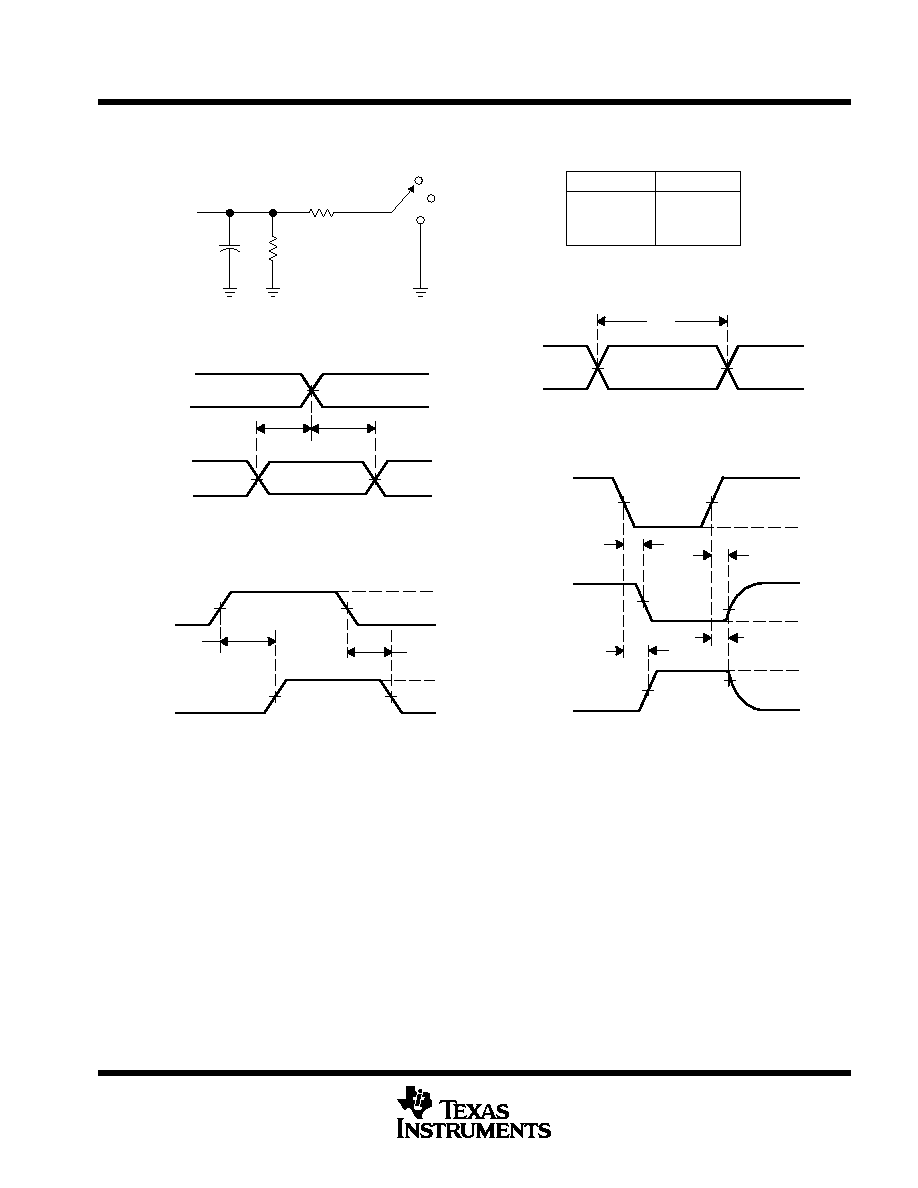
PARAMETER MEASUREMENT INFORMATION
V
CC
= 1.8 V
±
0.15 V
VCC/2
VCC/2
VCC/2
VCC/2
VCC/2
VCC/2
VCC/2
VCC/2
VOH
VOL
th
tsu
From Output
Under Test
CL = 30 pF
(see Note A)
LOAD CIRCUIT
S1
Open
GND
1k
1k
Output
Control
(low-level
enabling)
Output
Waveform 1
S1 at 2
×
VCC
(see Note B)
Output
Waveform 2
S1 at Open
(see Note B)
tPZL
tPZH
tPLZ
tPHZ
0 V
VOL + 0.15 V
VOH 0.15 V
0 V
VCC
0 V
0 V
tw
VCC
VCC
VOLTAGE WAVEFORMS
SETUP AND HOLD TIMES
VOLTAGE WAVEFORMS
PULSE DURATION
VOLTAGE WAVEFORMS
ENABLE AND DISABLE TIMES
Timing
Input
Data
Input
Input
tpd
tPLZ/tPZL
tPHZ/tPZH
Open
2
×
VCC
Open
TEST
S1
NOTES: A. CL includes probe and jig capacitance.
B. Waveform 1 is for an output with internal conditions such that the output is low except when disabled by the output control.
Waveform 2 is for an output with internal conditions such that the output is high except when disabled by the output control.
C. All input pulses are supplied by generators having the following characteristics: PRR
10 MHz, ZO = 50
, tr
2 ns, tf
2 ns.
D. The outputs are measured one at a time with one transition per measurement.
E. tPLZ and tPHZ are the same as tdis.
F. tPZL and tPZH are the same as ten.
G. tPLH and tPHL are the same as tpd.
0 V
VCC
VCC/2
tPHL
VCC/2
VCC/2
VCC
0 V
VOH
VOL
Input
Output
VOLTAGE WAVEFORMS
PROPAGATION DELAY TIMES
VCC/2
VCC/2
tPLH
2
×
VCC
VCC
Figure 1. Load Circuit and Voltage Waveforms
SN74LVC2952A
OCTAL BUS TRANSCEIVER AND REGISTER
WITH 3-STATE OUTPUTS
SCAS311F JANUARY 1993 REVISED JUNE 1998
8
POST OFFICE BOX 655303
·
DALLAS, TEXAS 75265
PARAMETER MEASUREMENT INFORMATION
V
CC
= 2.5 V
±
0.2 V
VCC/2
VCC/2
VCC/2
VCC/2
VCC/2
VCC/2
VCC/2
VCC/2
VOH
VOL
th
tsu
From Output
Under Test
CL = 30 pF
(see Note A)
LOAD CIRCUIT
S1
Open
GND
500
500
Output
Control
(low-level
enabling)
Output
Waveform 1
S1 at 2
×
VCC
(see Note B)
Output
Waveform 2
S1 at GND
(see Note B)
tPZL
tPZH
tPLZ
tPHZ
0 V
VOL + 0.15 V
VOH 0.15 V
0 V
VCC
0 V
0 V
tw
VCC
VCC
VOLTAGE WAVEFORMS
SETUP AND HOLD TIMES
VOLTAGE WAVEFORMS
PULSE DURATION
VOLTAGE WAVEFORMS
ENABLE AND DISABLE TIMES
Timing
Input
Data
Input
Input
tpd
tPLZ/tPZL
tPHZ/tPZH
Open
2
×
VCC
GND
TEST
S1
NOTES: A. CL includes probe and jig capacitance.
B. Waveform 1 is for an output with internal conditions such that the output is low except when disabled by the output control.
Waveform 2 is for an output with internal conditions such that the output is high except when disabled by the output control.
C. All input pulses are supplied by generators having the following characteristics: PRR
10 MHz, ZO = 50
, tr
2 ns, tf
2 ns.
D. The outputs are measured one at a time with one transition per measurement.
E. tPLZ and tPHZ are the same as tdis.
F. tPZL and tPZH are the same as ten.
G. tPLH and tPHL are the same as tpd.
0 V
VCC
VCC/2
tPHL
VCC/2
VCC/2
VCC
0 V
VOH
VOL
Input
Output
VOLTAGE WAVEFORMS
PROPAGATION DELAY TIMES
VCC/2
VCC/2
tPLH
2
×
VCC
VCC
Figure 2. Load Circuit and Voltage Waveforms
SN74LVC2952A
OCTAL BUS TRANSCEIVER AND REGISTER
WITH 3-STATE OUTPUTS
SCAS311F JANUARY 1993 REVISED JUNE 1998
9
POST OFFICE BOX 655303
·
DALLAS, TEXAS 75265
PARAMETER MEASUREMENT INFORMATION
V
CC
= 2.7 V AND 3.3 V
±
0.3 V
VOH
VOL
th
tsu
From Output
Under Test
CL = 50 pF
(see Note A)
LOAD CIRCUIT
S1
6 V
Open
GND
500
500
tPLH
tPHL
Output
Control
(low-level
enabling)
Output
Waveform 1
S1 at 6 V
(see Note B)
Output
Waveform 2
S1 at GND
(see Note B)
tPZL
tPZH
tPLZ
tPHZ
1.5 V
1.5 V
1.5 V
1.5 V
2.7 V
0 V
1.5 V
1.5 V
VOH
VOL
0 V
1.5 V
VOL + 0.3 V
1.5 V
VOH 0.3 V
0 V
1.5 V
2.7 V
0 V
1.5 V
1.5 V
0 V
2.7 V
0 V
1.5 V
1.5 V
tw
Input
2.7 V
2.7 V
3 V
VOLTAGE WAVEFORMS
SETUP AND HOLD TIMES
VOLTAGE WAVEFORMS
PROPAGATION DELAY TIMES
VOLTAGE WAVEFORMS
PULSE DURATION
VOLTAGE WAVEFORMS
ENABLE AND DISABLE TIMES
Timing
Input
Data
Input
Output
Input
tpd
tPLZ/tPZL
tPHZ/tPZH
Open
6 V
GND
TEST
S1
NOTES: A. CL includes probe and jig capacitance.
B. Waveform 1 is for an output with internal conditions such that the output is low except when disabled by the output control.
Waveform 2 is for an output with internal conditions such that the output is high except when disabled by the output control.
C. All input pulses are supplied by generators having the following characteristics: PRR
10 MHz, ZO = 50
, tr
2.5 ns, tf
2.5 ns.
D. The outputs are measured one at a time with one transition per measurement.
E. tPLZ and tPHZ are the same as tdis.
F. tPZL and tPZH are the same as ten.
G. tPLH and tPHL are the same as tpd.
Figure 3. Load Circuit and Voltage Waveforms

IMPORTANT NOTICE
Texas Instruments and its subsidiaries (TI) reserve the right to make changes to their products or to discontinue
any product or service without notice, and advise customers to obtain the latest version of relevant information
to verify, before placing orders, that information being relied on is current and complete. All products are sold
subject to the terms and conditions of sale supplied at the time of order acknowledgement, including those
pertaining to warranty, patent infringement, and limitation of liability.
TI warrants performance of its semiconductor products to the specifications applicable at the time of sale in
accordance with TI's standard warranty. Testing and other quality control techniques are utilized to the extent
TI deems necessary to support this warranty. Specific testing of all parameters of each device is not necessarily
performed, except those mandated by government requirements.
CERTAIN APPLICATIONS USING SEMICONDUCTOR PRODUCTS MAY INVOLVE POTENTIAL RISKS OF
DEATH, PERSONAL INJURY, OR SEVERE PROPERTY OR ENVIRONMENTAL DAMAGE ("CRITICAL
APPLICATIONS"). TI SEMICONDUCTOR PRODUCTS ARE NOT DESIGNED, AUTHORIZED, OR
WARRANTED TO BE SUITABLE FOR USE IN LIFE-SUPPORT DEVICES OR SYSTEMS OR OTHER
CRITICAL APPLICATIONS. INCLUSION OF TI PRODUCTS IN SUCH APPLICATIONS IS UNDERSTOOD TO
BE FULLY AT THE CUSTOMER'S RISK.
In order to minimize risks associated with the customer's applications, adequate design and operating
safeguards must be provided by the customer to minimize inherent or procedural hazards.
TI assumes no liability for applications assistance or customer product design. TI does not warrant or represent
that any license, either express or implied, is granted under any patent right, copyright, mask work right, or other
intellectual property right of TI covering or relating to any combination, machine, or process in which such
semiconductor products or services might be or are used. TI's publication of information regarding any third
party's products or services does not constitute TI's approval, warranty or endorsement thereof.
Copyright
©
1998, Texas Instruments Incorporated