
SN74LVC841A
10-BIT BUS-INTERFACE D-TYPE LATCH
WITH 3-STATE OUTPUTS
SCAS307H ≠ MARCH 1993 ≠ REVISED AUGUST 1998
1
POST OFFICE BOX 655303
∑
DALLAS, TEXAS 75265
D
EPIC
TM
(Enhanced-Performance Implanted
CMOS) Submicron Process
D
Typical V
OLP
(Output Ground Bounce)
< 0.8 V at V
CC
= 3.3 V, T
A
= 25
∞
C
D
Typical V
OHV
(Output V
OH
Undershoot)
> 2 V at V
CC
= 3.3 V, T
A
= 25
∞
C
D
Power Off Disables Outputs, Permitting
Live Insertion
D
Supports Mixed-Mode Signal Operation on
All Ports (5-V Input/Output Voltage With
3.3-V V
CC
)
D
ESD Protection Exceeds 2000 V Per
MIL-STD-883, Method 3015; Exceeds 200 V
Using Machine Model (C = 200 pF, R = 0)
D
Latch-Up Performance Exceeds 250 mA Per
JESD 17
D
Package Options Include Plastic
Small-Outline (DW), Shrink Small-Outline
(DB), and Thin Shrink Small-Outline (PW)
Packages
description
This 10-bit bus-interface D-type latch is designed for 1.65-V to 3.6-V V
CC
operation.
The SN74LVC841A is designed specifically for driving highly capacitive or relatively low-impedance loads. It
is particularly suitable for implementing buffer registers, I/O ports, bidirectional bus drivers, and
working registers.
The ten latches are transparent D-type latches. The device has noninverting data (D) inputs and provides true
data at its outputs.
A buffered output-enable (OE) input can be used to place the ten outputs in either a normal logic state (high
or low logic levels) or a high-impedance state. In the high-impedance state, the outputs neither load nor drive
the bus lines significantly. The high-impedance state and increased drive provide the capability to drive bus lines
without interface or pullup components.
OE does not affect the internal operations of the latch. Previously stored data can be retained or new data can
be entered while the outputs are in the high-impedance state.
Inputs can be driven from either 3.3-V or 5-V devices. This feature allows the use of these devices as translators
in a mixed 3.3-V/5-V system environment.
To ensure the high-impedance state during power up or power down, OE should be tied to V
CC
through a pullup
resistor; the minimum value of the resistor is determined by the current-sinking capability of the driver.
The SN74LVC841A is characterized for operation from ≠40
∞
C to 85
∞
C.
Copyright
©
1998, Texas Instruments Incorporated
PRODUCTION DATA information is current as of publication date.
Products conform to specifications per the terms of Texas Instruments
standard warranty. Production processing does not necessarily include
testing of all parameters.
Please be aware that an important notice concerning availability, standard warranty, and use in critical applications of
Texas Instruments semiconductor products and disclaimers thereto appears at the end of this data sheet.
EPIC is a trademark of Texas Instruments Incorporated.
DB, DW, OR PW PACKAGE
(TOP VIEW)
1
2
3
4
5
6
7
8
9
10
11
12
24
23
22
21
20
19
18
17
16
15
14
13
OE
1D
2D
3D
4D
5D
6D
7D
8D
9D
10D
GND
V
CC
1Q
2Q
3Q
4Q
5Q
6Q
7Q
8Q
9Q
10Q
LE

SN74LVC841A
10-BIT BUS-INTERFACE D-TYPE LATCH
WITH 3-STATE OUTPUTS
SCAS307H ≠ MARCH 1993 ≠ REVISED AUGUST 1998
2
POST OFFICE BOX 655303
∑
DALLAS, TEXAS 75265
FUNCTION TABLE
INPUTS
OUTPUT
OE
LE
D
Q
L
H
H
H
L
H
L
L
L
L
X
Q0
H
X
X
Z
logic symbol
This symbol is in accordance with ANSI/IEEE Std 91-1984 and IEC Publication 617-12.
EN
1
7
6D
8
7D
9
8D
10
9D
1D
2
1D
6Q
18
7Q
17
8Q
16
9Q
15
1Q
23
3
2D
4
3D
5
4D
6
5D
2Q
22
3Q
21
4Q
20
5Q
19
OE
C1
13
LE
11
10D
10Q
14
logic diagram (positive logic)
OE
To Nine Other Channels
1
13
2
23
LE
1D
C1
1D
1Q
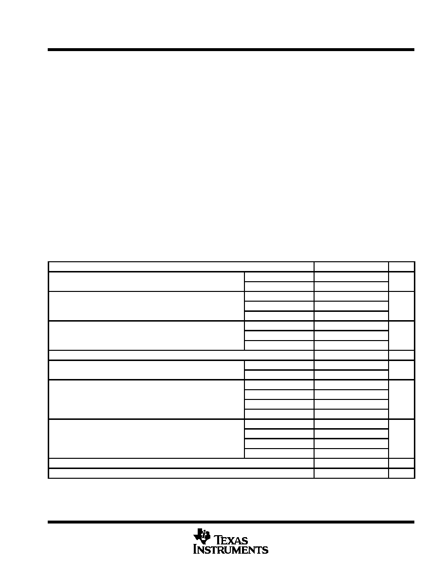
SN74LVC841A
10-BIT BUS-INTERFACE D-TYPE LATCH
WITH 3-STATE OUTPUTS
SCAS307H ≠ MARCH 1993 ≠ REVISED AUGUST 1998
3
POST OFFICE BOX 655303
∑
DALLAS, TEXAS 75265
absolute maximum ratings over operating free-air temperature range (unless otherwise noted)
Supply voltage range, V
CC
≠0.5 V to 6.5 V
. . . . . . . . . . . . . . . . . . . . . . . . . . . . . . . . . . . . . . . . . . . . . . . . . . . . . . . . .
Input voltage range, V
I
(see Note 1)
≠0.5 V to 6.5 V
. . . . . . . . . . . . . . . . . . . . . . . . . . . . . . . . . . . . . . . . . . . . . . . . .
Voltage range applied to any output in the high-impedance or power-off state, V
O
(see Note 1)
≠0.5 V to 6.5 V
. . . . . . . . . . . . . . . . . . . . . . . . . . . . . . . . . . . . . . . . . . . . . . . . . . . . . . . . . . . . . . . . . . .
Voltage range applied to any output in the high or low state, V
O
(see Notes 1 and 2)
≠0.5 V to V
CC
+ 0.5 V
. . . . . . . . . . . . . . . . . . . . . . . . . . . . . . . . . . . . . . . . . . . . . . . . . . . . . . .
Input clamp current, I
IK
(V
I
< 0)
≠50 mA
. . . . . . . . . . . . . . . . . . . . . . . . . . . . . . . . . . . . . . . . . . . . . . . . . . . . . . . . . . .
Output clamp current, I
OK
(V
O
< 0)
≠50 mA
. . . . . . . . . . . . . . . . . . . . . . . . . . . . . . . . . . . . . . . . . . . . . . . . . . . . . . . .
Continuous output current, I
O
±
50 mA
. . . . . . . . . . . . . . . . . . . . . . . . . . . . . . . . . . . . . . . . . . . . . . . . . . . . . . . . . . . . .
Continuous current through V
CC
or GND
±
100 mA
. . . . . . . . . . . . . . . . . . . . . . . . . . . . . . . . . . . . . . . . . . . . . . . . . .
Package thermal impedance,
JA
(see Note 3): DB package
104
∞
C/W
. . . . . . . . . . . . . . . . . . . . . . . . . . . . . . . .
DW package
81
∞
C/W
. . . . . . . . . . . . . . . . . . . . . . . . . . . . . . . . .
PW package
120
∞
C/W
. . . . . . . . . . . . . . . . . . . . . . . . . . . . . . . .
Storage temperature range, T
stg
≠65
∞
C to 150
∞
C
. . . . . . . . . . . . . . . . . . . . . . . . . . . . . . . . . . . . . . . . . . . . . . . . . . .
Stresses beyond those listed under "absolute maximum ratings" may cause permanent damage to the device. These are stress ratings only, and
functional operation of the device at these or any other conditions beyond those indicated under "recommended operating conditions" is not
implied. Exposure to absolute-maximum-rated conditions for extended periods may affect device reliability.
NOTES:
1. The input negative-voltage and output voltage ratings may be exceeded if the input and output current ratings are observed.
2. The value of VCC is provided in the recommended operating conditions table.
3. The package thermal impedance is calculated in accordance with JESD 51.
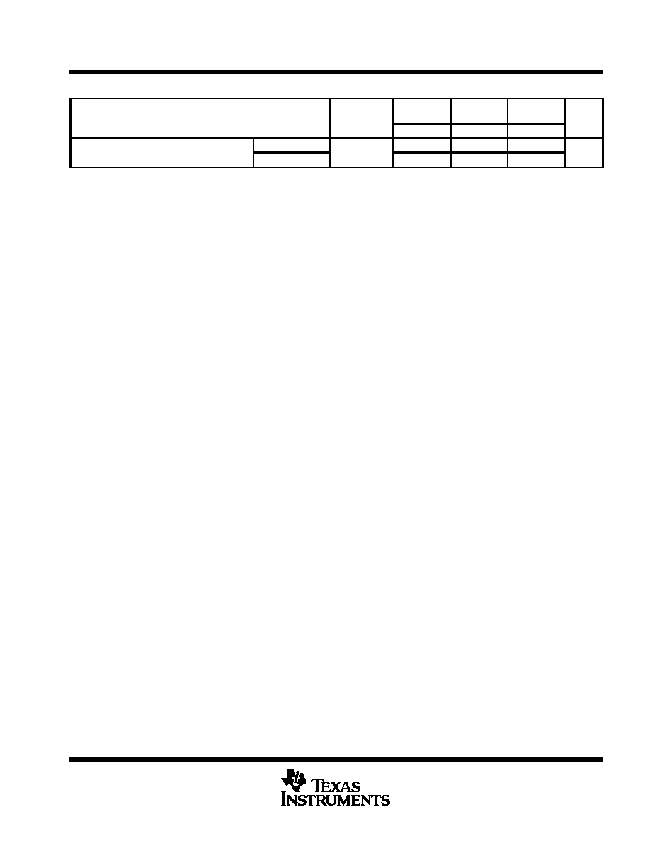
recommended operating conditions (see Note 4)
MIN
MAX
UNIT
VCC
Supply voltage
Operating
1.65
3.6
V
VCC
Supply voltage
Data retention only
1.5
V
VCC = 1.65 V to 1.95 V
0.65
◊
VCC
VIH
High-level input voltage
VCC = 2.3 V to 2.7 V
1.7
V
VCC = 2.7 V to 3.6 V
2
VCC = 1.65 V to 1.95 V
0.35
◊
VCC
VIL
Low-level input voltage
VCC = 2.3 V to 2.7 V
0.7
V
VCC = 2.7 V to 3.6 V
0.8
VI
Input voltage
0
5.5
V
VO
Output voltage
High or low state
0
VCC
V
VO
Output voltage
3 state
0
5.5
V
VCC = 1.65 V
≠4
IOH
High level output current
VCC = 2.3 V
≠8
mA
IOH
High-level output current
VCC = 2.7 V
≠12
mA
VCC = 3 V
≠24
VCC = 1.65 V
4
IOL
Low level output current
VCC = 2.3 V
8
mA
IOL
Low-level output current
VCC = 2.7 V
12
mA
VCC = 3 V
24
t/
v
Input transition rise or fall rate
0
10
ns/V
TA
Operating free-air temperature
≠40
85
∞
C
NOTE 4: All unused inputs of the device must be held at VCC or GND to ensure proper device operation. Refer to the TI application report,
Implications of Slow or Floating CMOS Inputs, literature number SCBA004.

SN74LVC841A
10-BIT BUS-INTERFACE D-TYPE LATCH
WITH 3-STATE OUTPUTS
SCAS307H ≠ MARCH 1993 ≠ REVISED AUGUST 1998
4
POST OFFICE BOX 655303
∑
DALLAS, TEXAS 75265
electrical characteristics over recommended operating free-air temperature range (unless
otherwise noted)
PARAMETER
TEST CONDITIONS
VCC
MIN
TYP
MAX
UNIT
IOH = ≠100
µ
A
1.65 V to 3.6 V
VCC≠0.2
IOH = ≠4 mA
1.65 V
1.2
VOH
IOH = ≠8 mA
2.3 V
1.7
V
VOH
IOH = 12 mA
2.7 V
2.2
V
IOH = ≠12 mA
3 V
2.4
IOH = ≠24 mA
3 V
2.2
IOL = 100
µ
A
1.65 V to 3.6 V
0.2
IOL = 4 mA
1.65 V
0.45
VOL
IOL = 8 mA
2.3 V
0.7
V
IOL = 12 mA
2.7 V
0.4
IOL = 24 mA
3 V
0.55
II
VI = 0 to 5.5 V
3.6 V
±
5
µ
A
Ioff
VI or VO = 5.5 V
0
±
10
µ
A
IOZ
VO = 0 to 5.5 V
3.6 V
±
10
µ
A
ICC
VI = VCC or GND
IO = 0
3 6 V
10
µ
A
ICC
3.6 V
VI
5.5 V
IO = 0
3.6 V
10
µ
A
ICC
One input at VCC ≠ 0.6 V,
Other inputs at VCC or GND
2.7 V to 3.6 V
500
µ
A
Ci
VI = VCC or GND
3.3 V
5
pF
Co
VO = VCC or GND
3.3 V
7
pF
All typical values are at VCC = 3.3 V, TA = 25
∞
C.
This applies in the disabled state only.
timing requirements over recommended operating free-air temperature range (unless otherwise
noted) (see Figures 1 through 3)
VCC = 1.8 V
±
0.15 V
VCC = 2.5 V
±
0.2 V
VCC = 2.7 V
VCC = 3.3 V
±
0.3 V
UNIT
MIN
MAX
MIN
MAX
MIN
MAX
MIN
MAX
tw
Pulse duration
ß
ß
3.3
3.3
ns
tsu
Setup time, data before LE
ß
ß
2.1
2.1
ns
th
Hold time, data after LE
ß
ß
1
1
ns
ß This information was not available at the time of publication.
switching characteristics over recommended operating free-air temperature range (unless
otherwise noted) (see Figures 1 through 3)
PARAMETER
FROM
(INPUT)
TO
(OUTPUT)
VCC = 1.8 V
±
0.2 V
VCC = 2.5 V
±
0.2 V
VCC = 2.7 V
VCC = 3.3 V
±
0.3 V
UNIT
(INPUT)
(OUTPUT)
MIN
MAX
MIN
MAX
MIN
MAX
MIN
MAX
t d
D
Q
ß
ß
ß
ß
7.5
2.4
6.7
ns
tpd
LE
Q
ß
ß
ß
ß
8.6
2.7
7.6
ns
ten
OE
Q
ß
ß
ß
ß
8.5
1.3
7.2
ns
tdis
OE
Q
ß
ß
ß
ß
6.6
1.9
5.9
ns
tsk(o)∂
1
ns
ß This information was not available at the time of publication.
∂ Skew between any two outputs of the same package switching in the same direction
SN74LVC841A
10-BIT BUS-INTERFACE D-TYPE LATCH
WITH 3-STATE OUTPUTS
SCAS307H ≠ MARCH 1993 ≠ REVISED AUGUST 1998
5
POST OFFICE BOX 655303
∑
DALLAS, TEXAS 75265
operating characteristics, T
A
= 25
∞
C
PARAMETER
TEST
CONDITIONS
VCC = 1.8 V
±
0.15 V
VCC = 2.5 V
±
0.2 V
VCC = 3.3 V
±
0.3 V
UNIT
CONDITIONS
TYP
TYP
TYP
Cpd
Power dissipation capacitance
Outputs enabled
f = 10 MHz
25
pF
Cpd
per latch
Outputs disabled
f = 10 MHz
6
pF
This information was not available at the time of publication.