 | –≠–ª–µ–∫—Ç—Ä–æ–Ω–Ω—ã–π –∫–æ–º–ø–æ–Ω–µ–Ω—Ç: THS1207 | –°–∫–∞—á–∞—Ç—å:  PDF PDF  ZIP ZIP |
Document Outline
- FEATURES
- APPLICATIONS
- DESCRIPTION
- ORDERING INFORMATION
- ABSOLUTE MAXIMUM RATINGS
- RECOMMENDED OPERATING CONDITIONS
- ELECTRICAL CHARACTERISTICS
- TIMING REQUIREMENTS
- Terminal Functions
- FUNCTIONAL BLOCK DIAGRAM
- TYPICAL CHARACTERISTICS
- DETAILED DESCRIPTION
- Reference Voltage
- Analog Inputs
- Converter
- Conversion Clock
- SYNC
- Sampling Rate
- Conversion
- DIGITAL OUTPUT DATA FORMAT
- ADC CONTROL REGISTER
- Writing to Control Register 0 and Control Register 1
- Control Register 0 (see Table 7)
- ANALOG INPUT CHANNEL SELECTION
- Test Mode
- Control Register 1 (see Table 7)
- TIMING AND SIGNAL DESCRIPTION OF THE THS1207
- Read Timing (using RD\, RD\-controlled)
- Read Timing Parameter (RD\-controlled)
- Write Timing (using WR\, WR\-controlled)
- Write Timing Parameter Using WR\ (WR\-controlled)
- Read Timing (using R/W\, (CS0)\-controlled)
- Read Timing Parameter ((CS0)\-controlled)
- Write Timing Diagram (using R/W\, (CS0)\-controlled)
- Write Timing Parameter ((CS0)\-controlled)
- ANALOG INPUT CONFIGURATION AND REFERENCE VOLTAGE
- SINGLE-ENDED MODE OF OPERATION
- DC-COUPLING
- DIFFERENTIAL MODE OF OPERATION
- DEFINITIONS OF SPECIFICATIONS AND TERMINOLOGY
- Integral Nonlinearity
- Differential Nonlinearity
- Zero Offset
- Gain Error
- Signal-to-Noise Ratio + Distortion (SINAD)
- Effective Number Of Bits (ENOB)
- Total Harmonic Distortion (THD)
- Spurious Free Dynamic Range (SFDR)
- MECHANICAL DATA
- DA (R-PDSO-G**) PLASTIC SMALL-OUTLINE PACKAGE
THS1207
SLAS284A ≠ AUGUST 2000 ≠ REVISED DECEMBER 2002
12 BIT 4 ANALOG INPUT, 6 MSPS, SIMULTANEOUS SAMPLING
ANALOG TO DIGITAL CONVERTER
FEATURES
D
Simultaneous Sampling of 4 Single-Ended
Signals or 2 Differential Signals or
Combination of Both
D
Signal-to-Noise and Distortion Ratio:
68 dB at f
I
= 2 MHz
D
Differential Nonlinearity Error:
±
1 LSB
D
Integral Nonlinearity Error:
±
1.5 LSB
D
Auto-Scan Mode for 2, 3, or 4 Inputs
D
3-V or 5-V Digital Interface Compatible
D
Low Power: 216 mW Max at 5 V
D
Power Down: 1 mW Max
D
5-V Analog Single Supply Operation
D
Internal Voltage References . . . 50 PPM/
∞
C
and
±
5% Accuracy
D
Glueless DSP Interface
D
Parallel
µ
C/DSP Interface
APPLICATIONS
D
Radar Applications
D
Communications
D
Control Applications
D
High-Speed DSP Front-End
D
Automotive Applications
DESCRIPTION
The THS1207 is a CMOS, low-power, 12-bit, 6 MSPS
analog-to-digital converter (ADC). The speed,
resolution, bandwidth, and single-supply operation are
suited for applications in radar, imaging, high-speed
acquisition, and communications. A multistage
pipelined architecture with output error correction logic
provides for no missing codes over the full operating
temperature range. Internal control registers are used
to program the ADC into the desired mode. The
THS1207 consists of four analog inputs, which are
sampled simultaneously. These inputs can be selected
individually and configured to single-ended or
differential-inputs. Internal reference voltages for the
ADC (1.5 V and 3.5 V) are provided. An external
reference can also be chosen to suit the dc accuracy
and temperature drift requirements of the application.
The THS1207C is characterized for operation from 0
∞
C
to 70
∞
C, the THS1207I is characterized for operation
from ≠40
∞
C to 85
∞
C.
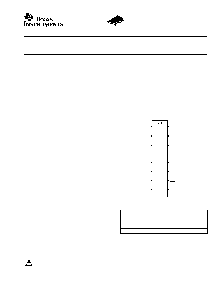
1
2
3
4
5
6
7
8
9
10
11
12
13
14
15
16
32
31
30
29
28
27
26
25
24
23
22
21
20
19
18
17
D0
D1
D2
D3
D4
D5
BV
DD
BGND
D6
D7
D8
D9
D10/RA0
D11/RA1
CONV_CLK
SYNC
AINP
AINM
BINP
BINM
REFIN
REFOUT
REFP
REFM
AGND
AV
DD
CS0
CS1
WR (R/W)
RD
DV
DD
DGND
DA PACKAGE
(TOP VIEW)
ORDERING INFORMATION
PACKAGED DEVICE
TA
TSSOP
(DA)
0
∞
C to 70
∞
C
THS1207CDA
≠40
∞
C to 85
∞
C
THS1207IDA
PRODUCTION DATA information is current as of publication date. Products
conform to specifications per the terms of Texas Instruments standard warranty.
Production processing does not necessarily include testing of all parameters.
Please be aware that an important notice concerning availability, standard warranty, and use in critical applications of Texas Instruments
semiconductor products and disclaimers thereto appears at the end of this data sheet.
www.ti.com
Copyright
2002, Texas Instruments Incorporated

THS1207
SLAS284A ≠ AUGUST 2000 ≠ REVISED DECEMBER 2002
www.ti.com
2
These devices have limited built-in ESD protection. The leads should be shorted together or the device placed in conductive foam during
storage or handling to prevent electrostatic damage to the MOS gates.
ABSOLUTE MAXIMUM RATINGS
over operating free-air temperature range unless otherwise noted(1)
UNITS
DGND to DVDD
≠0.3 V to 6.5 V
Supply voltage range
BGND to BVDD
≠0.3 V to 6.5 V
Su
ly voltage range
AGND to AVDD
≠0.3 V to 6.5 V
Analog input voltage range
AGND ≠0.3 V to AVDD + 1.5 V
Reference input voltage
≠0.3 V + AGND to AVDD + 0.3 V
Digital input voltage range
≠0.3 V to BVDD/DVDD + 0.3 V
Operating virtual junction temperature range, TJ
≠40
∞
C to 150
∞
C
Operating free air temperature range T
THS1207C
0
∞
C to 70
∞
C
Operating free-air temperature range, TA
THS1207I
≠40
∞
C to 85
∞
C
Storage temperature range, Tstg
≠65
∞
C to 150
∞
C
Lead temperature 1,6 mm (1/16 inch) from case for 10 seconds
260
∞
C
(1) Stresses beyond those listed under "absolute maximum ratings" may cause permanent damage to the device. These are stress ratings only, and
functional operation of the device at these or any other conditions beyond those indicated under "recommended operating conditions" is not
implied. Exposure to absolute-maximum-rated conditions for extended periods may affect device reliability.
RECOMMENDED OPERATING CONDITIONS
POWER SUPPLY
MIN
NOM
MAX
UNIT
AVDD
4.75
5
5.25
Supply voltage
DVDD
4.75
5
5.25
V
y
g
BVDD
3
5.25
ANALOG AND REFERENCE INPUTS
MIN
NOM
MAX
UNIT
Analog input voltage in single-ended configuration
VREFM
VREFP
V
Common-mode input voltage VCM in differential configuration
1
2.5
4
V
External reference voltage,VREFP (optional)
3.5
AVDD≠1.2
V
External reference voltage, VREFM (optional)
1.4
1.5
V
Input voltage difference, REFP ≠ REFM
2
V
DIGITAL INPUTS
MIN
NOM
MAX
UNIT
High level input voltage V
BVDD = 3.3 V
2
V
High-level input voltage, VIH
BVDD = 5.25 V
2.6
V
Low level input voltage V
BVDD = 3.3 V
0.6
V
Low-level input voltage, VIL
BVDD = 5.25 V
0.6
V
Input CONV_CLK frequency
DVDD = 4.75 V to 5.25 V
0.1
6
MHz
CONV_CLK pulse duration, clock high, tw(CONV_CLKH)
DVDD = 4.75 V to 5.25 V
80
83
5000
ns
CONV_CLK pulse duration, clock low, tw(CONV_CLKL)
DVDD = 4.75 V to 5.25 V
80
83
5000
ns
Operating free air temperature T
THS1207CDA
0
70
∞
C
Operating free-air temperature, TA
THS1207IDA
≠40
85
∞
C
THS1207
SLAS284A ≠ AUGUST 2000 ≠ REVISED DECEMBER 2002
www.ti.com
3
ELECTRICAL CHARACTERISTICS
over recommended operating conditions, AVDD = DVDD = 5 V, BVDD = 3.3 V, VREWF = internal (unless otherwise noted)
DIGITAL SPECIFICATIONS
PARAMETER
TEST CONDITIONS
MIN
TYP
MAX
UNIT
Digital inputs
IIH
High-level input current
DVDD = digital inputs
≠50
50
µ
A
IIL
Low-level input current
Digital input = 0 V
≠50
50
µ
A
Ci
Input capacitance
5
pF
Digital outputs
VOH
High-level output voltage
IOH = ≠50
µ
A
BV
3 3 V 5 V
BVDD≠0.5
V
VOL
Low-level output voltage
IOL = 50
µ
A
BVDD = 3.3 V, 5 V
0.4
V
IOZ
High-impedance-state output current
CS1 = DGND,
CS0 = DVDD
≠10
10
µ
A
CO
Output capacitance
5
pF
CL
Load capacitance at databus D0 ≠ D11
30
pF
ELECTRICAL CHARACTERISTICS
over recommended operating conditions, AVDD = DVDD = 5 V, BVDD = 3.3 V, fs = 6 MSPS, VREF = internal (unless otherwise noted)
DC SPECIFICATIONS
PARAMETER
TEST CONDITIONS
MIN
TYP
MAX
UNIT
Resolution
12
Bits
Accuracy
Integral nonlinearity, INL
±
1.5
LSB
Differential nonlinearity, DNL
±
1
LSB
Offset error
After calibration in single-ended mode
20
LSB
Offset error
After calibration in differential mode
≠20
20
LSB
Gain error
≠20
20
LSB
Analog input
Input capacitance
15
pF
Input leakage current
VAIN = VREFM to VREFP
±
10
µ
A
Internal voltage reference
Accuracy, VREFP
3.3
3.5
3.7
V
Accuracy, VREFM
1.4
1.5
1.6
V
Temperature coefficient
50
PPM/
∞
C
Reference noise
100
µ
V
Accuracy, REFOUT
2.475
2.5
2.525
V
Power supply
IDDA
Analog supply current
AVDD = DVDD = 5 V, BVDD =3.3 V
36
40
mA
IDDD
Digital supply current
AVDD = DVDD = 5 V, BVDD = 3.3 V
0.5
3
mA
IDDB
Buffer supply current
AVDD = DVDD = 5 V, BVDD = 3.3 V
1.5
4
mA
Power dissipation
AVDD = DVDD = 5 V, BVDD = 3.3 V
186
216
mW
Power dissipation in power down with conversion
clock inactive
AVDD = DVDD = 5 V, BVDD = 3.3 V
0.25
mW

THS1207
SLAS284A ≠ AUGUST 2000 ≠ REVISED DECEMBER 2002
www.ti.com
4
ELECTRICAL CHARACTERISTICS
over recommended operating conditions, VREF = internal, fs = 6 MSPS, fI = 2 MHz at ≠1 dBFS (unless otherwise noted)
AC SPECIFICATIONS, AVDD = DVDD = 5 V, BVDD = 3.3 V, CL < 30 pF
PARAMETER
TEST CONDITIONS
MIN
TYP
MAX
UNIT
SINAD
Signal to noise ratio + distortion
Differential mode
63
63
dB
SINAD
Signal-to-noise ratio + distortion
Single-ended mode
62
64
dB
SNR
Signal to noise ratio
Differential mode
64
69
dB
SNR
Signal-to-noise ratio
Single-ended mode
64
68
dB
THD
Total harmonic distortion
Differential mode
≠70
≠67
dB
THD
Total harmonic distortion
Single-ended mode
≠68
≠64
dB
ENOB
Effective number of bits
Differential mode
10.17
10.5
Bits
ENOB
Effective number of bits
Single-ended mode
10
10.3
Bits
SFDR
Spurious free dynamic range
Differential mode
67
71
dB
SFDR
Spurious free dynamic range
Single-ended mode
65
69
dB
Analog Input
Full-power bandwidth with a source impedance of 150
in
differential configuration.
Full scale sinewave
3 dB
96
MHz
Full-power bandwidth with a source impedance of 150
in
single-ended configuration.
Full scale sinewave, ≠3 dB
54
MHz
Small-signal bandwidth with a source impedance of 150
in
differential configuration.
100 mVpp sinewave
3 dB
96
MHz
Small-signal bandwidth with a source impedance of 150
in
single-ended configuration.
100 mVpp sinewave, ≠3 dB
54
MHz
TIMING REQUIREMENTS
AVDD = DVDD = 5 V, BVDD = 3.3 V, VREF = internal, CL < 30 pF
PARAMETER
TEST CONDITIONS
MIN
TYP
MAX
UNIT
tpipe
Latency
5
CONV
CLK
tsu(CONV_CLKL-READL)
Setup time, CONV_CLK low before CS valid
10
ns
tsu(READH-CONV_CLKL)
Setup time, CS invalid to CONV_CLK low
20
ns
td(CONV_CLKL-SYNCL)
Delay time, CONV_CLK low to SYNC low
10
ns
td(CONV_CLKL-SYNCH)
Delay time, CONV_CLK low to SYNC high
10
ns
THS1207
SLAS284A ≠ AUGUST 2000 ≠ REVISED DECEMBER 2002
www.ti.com
5
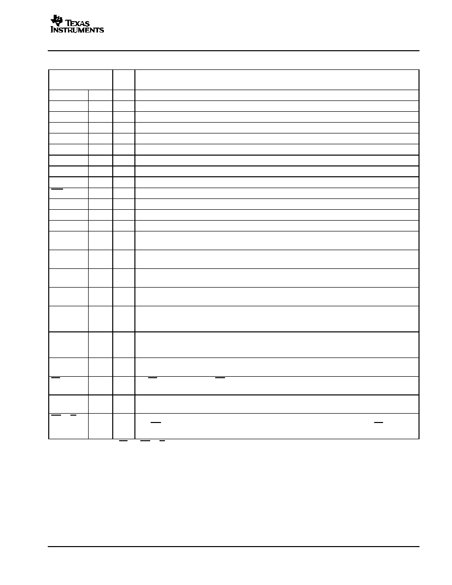
Terminal Functions
TERMINAL
I/O
DESCRIPTION
NAME
NO.
I/O
DESCRIPTION
AINP
32
I
Analog input, single-ended or positive input of differential channel A
AINM
31
I
Analog input, single-ended or negative input of differential channel A
BINP
30
I
Analog input, single-ended or positive input of differential channel B
BINM
29
I
Analog input, single-ended or negative input of differential channel B
AVDD
23
I
Analog supply voltage
AGND
24
I
Analog ground
BVDD
7
I
Digital supply voltage for buffer
BGND
8
I
Digital ground for buffer
CONV_CLK
15
I
Digital input. This input is the conversion clock input.
CS0
22
I
Chip select input (active low)
CS1
21
I
Chip select input (active high)
DGND
17
I
Digital ground. Ground reference for digital circuitry.
DVDD
18
I
Digital supply voltage
D0 ≠ D9
1≠6,
9≠12
I/O/Z
Digital input, output; D0 = LSB
D10/RA0
13
I/O/Z
Digital input, output. The data line D10 is also used as an address line (RA0) for the control register. This is
required for writing to the control register 0 and control register 1. See Table 7.
D11/RA1
14
I/O/Z
Digital input, output (D11 = MSB). The data line D11 is also used as an address line (RA1) for the control register.
This is required for writing to control register 0 and control register 1. See Table 7.
REFIN
28
I
Common-mode reference input for the analog input channels. It is recommended that this pin be connected to the
reference output REFOUT.
REFP
26
I
Reference input, requires a bypass capacitor of 10
µ
F to AGND in order to bypass the internal reference voltage.
An external reference voltage at this input can be applied. This option can be programmed through control
register 0. See Table 8.
REFM
25
I
Reference input, requires a bypass capacitor of 10
µ
F to AGND in order to bypass the internal reference voltage.
An external reference voltage at this input can be applied. This option can be programmed through control
register 0. See Table 8.
REFOUT
27
O
Analog fixed reference output voltage of 2.5 V. Sink and source capability of 250
µ
A. The reference output
requires a capacitor of 10
µ
F to AGND for filtering and stability.
RD(1)
19
I
The RD input is used only if the WR input is configured as a write only input. In this case, it is a digital input, active
low as a data read select from the processor. See timing section.
SYNC
16
O
Synchronization output. This signal indicates in a multichannel operation that data of channel A is brought to the
digital output and can therefore be used for synchronization.
WR (R/W)(1)
20
I
This input is programmable. It functions as a read-write input R/W and can also be configured as a write-only
input WR, which is active low and used as data write select from the processor. In this case, the RD input is used
as a read input from the processor. See timing section.
(1) The start-conditions of RD and WR (R/W) are unknown. The first access to the ADC has to be a write access to initialize the ADC.