 | –≠–ª–µ–∫—Ç—Ä–æ–Ω–Ω—ã–π –∫–æ–º–ø–æ–Ω–µ–Ω—Ç: THS1215 | –°–∫–∞—á–∞—Ç—å:  PDF PDF  ZIP ZIP |

www.ti.com
FEATURES
APPLICATIONS
1
2
3
4
5
6
7
8
9
10
11
12
13
14
28
27
26
25
24
23
22
21
20
19
18
17
16
15
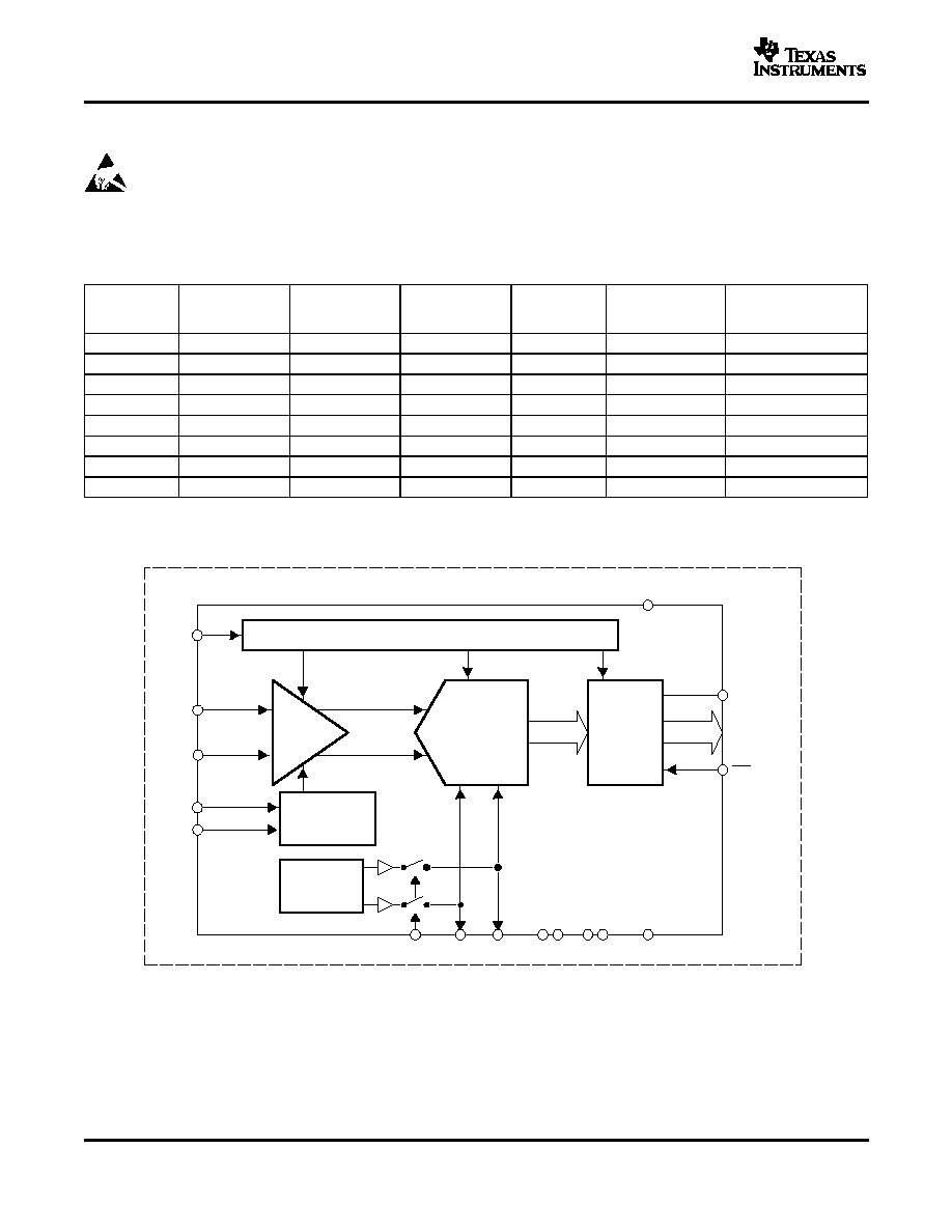
AGND
CON1
CON0
EXTREF
AIN+
AIN-
AGND
AV
DD
REFT
REFB
OVRNG
D11
D10
D9
CLK
AV
DD
OE
D0
D1
D2
D3
D4
DV
DD
DGND
D5
D6
D7
D8
DW OR PW PACKAGE
(TOP VIEW)
DESCRIPTION
THS1215
SLAS292A ≠ MARCH 2001 ≠ REVISED MARCH 2004
3.3-V, 12-BIT, 15 MSPS, LOW-POWER ANALOG-TO-DIGITAL
CONVERTER WITH POWER DOWN
∑
Input Configurations:
≠ Differential 0.5x Gain
≠ Differential 1x Gain
∑
3.3-V Supply Operation
∑
Internal Voltage Reference
∑
Out-of-Range Indicator
∑
Power-Down Mode
∑
Camcorders
∑
Digital Cameras
∑
Copiers
∑
Communications
∑
Test Instruments
∑
Baseband Digitization
The THS1215 is a CMOS, low-power, 12-bit, 15 MSPS analog-to-digital converter (ADC) that operates with a
3.3-V supply. The THS1215 gives circuit developers complete flexibility. The analog input to the THS1215 is
differential with a gain of 1.0 in Mode 1 and 0.5 in Mode 2. The THS1215 provides a wide selection of voltage
references to match the user's design requirements. For more design flexibility, the internal reference can be
bypassed to use an external reference to suit the dc accuracy and temperature drift requirements of the
application. The out-of-range output is used to monitor any out-of-range condition in the THS1215's input range.
The speed, resolution, and single-supply operation of the THS1215 are suited for applications in video,
multimedia, high-speed acquisition, and communications. The speed and resolution ideally suit charge-couple
device (CCD) input systems such as digital copiers, digital cameras, and camcorders. The wide input voltage
range between V
REFB
and V
REFT
allows the THS1215 to be designed into multiple systems.
The THS1215C is characterized for operation from 0
∞
C to 70
∞
C. The THS1215I is characterized for operation
from -40
∞
C to 85
∞
C.
Please be aware that an important notice concerning availability, standard warranty, and use in critical applications of Texas
Instruments semiconductor products and disclaimers thereto appears at the end of this data sheet.
PRODUCTION DATA information is current as of publication date.
Copyright © 2001≠2004, Texas Instruments Incorporated
Products conform to specifications per the terms of the Texas
Instruments standard warranty. Production processing does not
necessarily include testing of all parameters.
www.ti.com
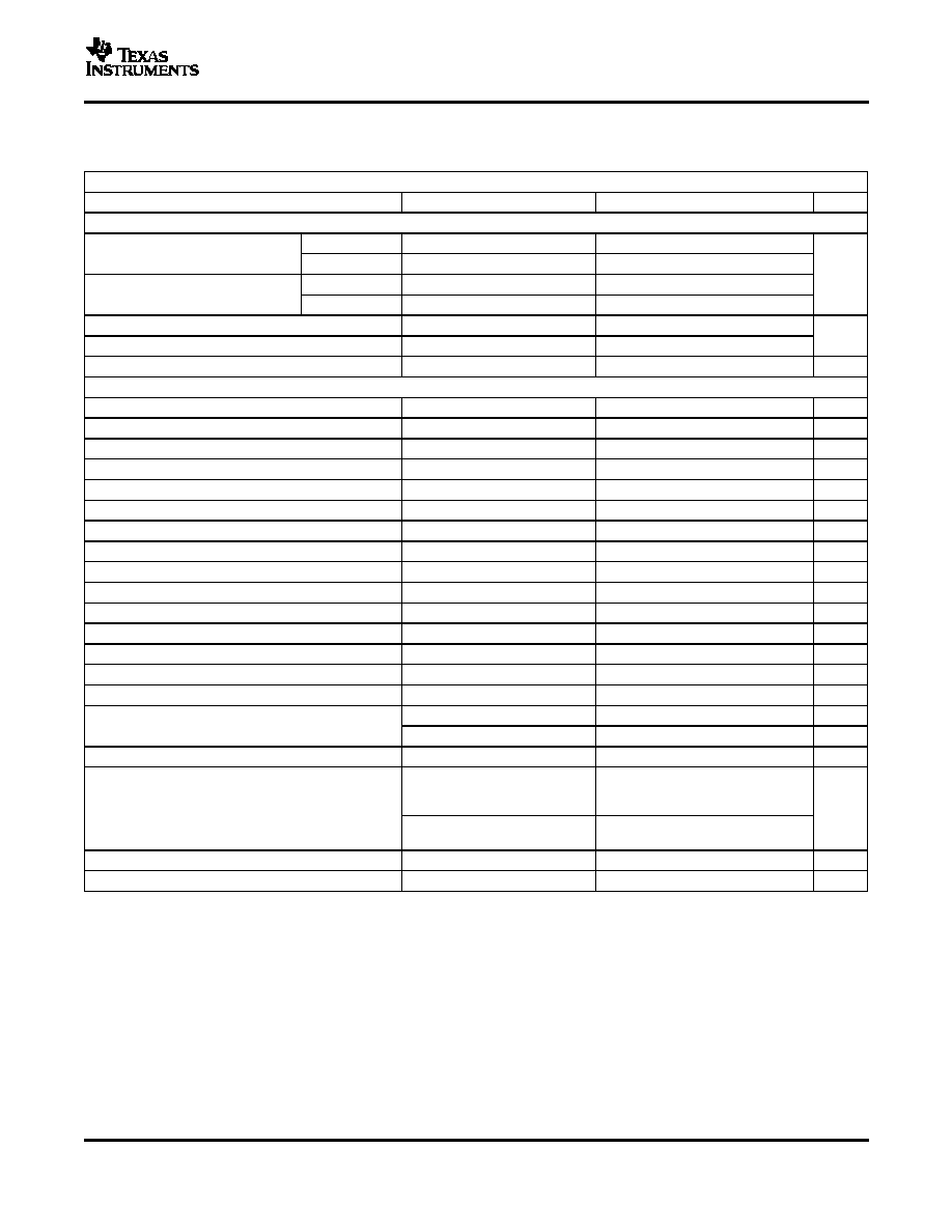
FUNCTIONAL BLOCK DIAGRAM
12-Bit ADC
D[11:0]
Sample
and Hold
CLK
DGND
AGND
OVRNG
CON0
Timing Circuitry
REFT REFB
Internal
Reference
Circuit
CON1
3-State
Output
Buffers
EXTREF
Configuration
Control
Circuit
DV
DD
AIN+
AIN-
AV
DD
OE
THS1215
SLAS292A ≠ MARCH 2001 ≠ REVISED MARCH 2004
This integrated circuit can be damaged by ESD. Texas Instruments recommends that all integrated
circuits be handled with appropriate precautions. Failure to observe proper handling and installation
procedures can cause damage.
ESD damage can range from subtle performance degradation to complete device failure. Precision
integrated circuits may be more susceptible to damage because very small parametric changes could
cause the device not to meet its published specifications.
ORDERING INFORMATION
PRODUCT
PACKAGE-
PACKAGE
SPECIFIED
PACKAGE
ORDERING
TRANSPORT
LEAD
DESIGNATOR
(1)
TEMPERATURE
MARKING
NUMBER
MEDIA, QUANTITY
RANGE
THS1215
TSSOP-28
PW
0
∞
C TO 70
∞
C
TH1215
THS1215 CPW
Tube, 50
THS1215
TSSOP-28
PW
0
∞
C TO 70
∞
C
TH1215
THS1215 CPWR
Tape and reel, 2000
THS1215
TSSOP-28
PW
≠40
∞
C TO 85
∞
C
TJ1215
THS1215 IPW
Tube, 50
THS1215
TSSOP-28
PW
≠40
∞
C TO 85
∞
C
TJ1215
THS1215 IPWR
Tape and reel, 2000
THS1215
SOP-28
DW
0
∞
C TO 70
∞
C
TH1215
THS1215 CDW
Tube, 20
THS1215
SOP-28
DW
0
∞
C TO 70
∞
C
TH1215
THS1215 CDWR
Tape and reel, 1000
THS1215
SOP-28
DW
≠40
∞
C TO 85
∞
C
TJ1215
THS1215 IDW
Tube, 20
THS1215
SOP-28
DW
≠40
∞
C TO 85
∞
C
TJ1215
THS1215 IDWR
Tape and reel, 1000
(1)
For the most current specifications and package information refer to our Web site at www.ti.com.
2

www.ti.com
TERMINAL FUNCTIONS
ABSOLUTE MAXIMUM RATINGS
(1)
THS1215
SLAS292A ≠ MARCH 2001 ≠ REVISED MARCH 2004
TERMINAL
I/O
DESCRIPTION
NAME
NO.
AGND
1, 7
I
Analog ground
AV
DD
8, 27
I
Analog supply
AIN+
5
I
Positive analog input
AIN-
6
I
Negative analog input
CLK
28
I
ADC conversion clock
CON1
2
I
Configuration input 1
CON0
3
I
Configuration input 0
DGND
19
I
Digital ground
DV
DD
20
I
Digital supply
D11
12
O
ADC data bit 11
D10
13
O
ADC data bit 10
D9
14
O
ADC data bit 9
D8
15
O
ADC data bit 8
D7
16
O
ADC data bit 7
D6
17
O
ADC data bit 6
D5
18
O
ADC data bit 5
D4
21
O
ADC data bit 4
D3
22
O
ADC data bit 3
D2
23
O
ADC data bit 2
D1
24
O
ADC data bit 1
D0
25
O
ADC data bit 0
EXTREF
4
I
Reference select input (high = external, low = internal)
OVRNG
11
O
Out of range indicator (high = out of range)
OE
26
I
Output enable (high = disable, low = enable)
REFT
9
I/O
Upper ADC reference voltage
REFB
10
I/O
Lower ADC reference voltage
over operating free-air temperature range (unless otherwise noted)
UNIT
AV
DD
to AGND, DV
DD
to DGND
≠0.3 V to 4 V
Supply voltage range
AGND to DGND
≠0.3 V to 0.3 V
Reference voltage input range, REFT, REFB to AGND
≠0.3 to AV
DD
+ 0.3 V
Analog input voltage range, AIN+, AIN≠ to AGND
≠0.3 to AV
DD
+ 0.3 V
Clock input voltage range, CLK to AGND
≠0.3 to AV
DD
+ 0.3 V
Digital input voltage range, digital input to DGND
≠0.3 to DV
DD
+ 0.3 V
Digital output voltage range, digital output to DGND
≠0.3 to DV
DD
+ 0.3 V
Operating junction temperature range, T
J
≠40
∞
C to 150
∞
C
Storage temperature range, T
STG
≠65
∞
C to 150
∞
C
Lead temperature 1,6 mm (1/16 in) from case for 10 seconds
300
∞
C
(1)
Stresses beyond those listed under "absolute maximum ratings" may cause permanent damage to the device. These are stress ratings
only, and functional operation of the device at these or any other conditions beyond those indicated under "recommended operating
conditions" is not implied. Exposure to absolute-maximum-rated conditions for extended periods may affect device reliability.
3

www.ti.com
RECOMMENDED OPERATING CONDITIONS
THS1215
SLAS292A ≠ MARCH 2001 ≠ REVISED MARCH 2004
over operating free-air temperature range, T
A
(unless otherwise noted)
MIN
NOM
MAX
UNIT
POWER SUPPLY
Supply voltage
AV
DD
3.0
3.3
3.6
V
DV
DD
ANALOG AND REFERENCE INPUTS
V
REFT
f
CLK
= 5 MHz to 15 MHz
2.0
2.15
2.5
Reference input voltage
V
V
REFB
f
CLK
= 5 MHz to 15 MHz
1.05
1.15
1.3
Reference voltage differential, V
REFT
≠ V
REFB
f
CLK
= 5 MHz to 15 MHz
0.95
1.0
1.05
V
CON1 = 0, CON0 = 1
≠1.0
1.0
V
Analog input voltage differential, (AIN+) ≠ (AIN≠)
(1)
CON1 = 1, CON0 = 0
≠2.0
2.0
V
Analog input capacitance, C
i
10
pF
Clock input
(2)
0
AV
DD
V
DIGITAL OUTPUTS
Minimum digital output load resistance, R
L
100
k
Maximum digital output load capacitance, C
i
0
10
15
pF
DIGITAL INPUTS
High-level input voltage, V
IH
2.4
DV
DD
V
Low-level input voltage, V
IL
DGND
0.8
V
Clock frequency, f
CLK
, See Note
(3)
5
30
MHz
Clock pulse duration, t
W(CLKL)
, t
W(CLKH)
f
CLK
= 15 MHz
30
33.3
36.7
ns
TH1215
0
70
∞
C
Operating free-air temperature, T
A
TJ1215
≠40
85
(1)
Based on V
REFT
≠ V
REFB
= 1.0 V, varies proportional to the V
REFT
≠ V
REFB
value. AIN+ and AIN≠ inputs must always be greater than 0 V
and less than AV
DD
.
(2)
Clock pin is referenced to AGND and powered by AV
DD
.
(3)
Clock frequency can be extended to this range without degradation of performance.
4
www.ti.com
ELECTRICAL CHARACTERISTICS
THS1215
SLAS292A ≠ MARCH 2001 ≠ REVISED MARCH 2004
over recommended operating conditions (AV
DD
= DV
DD
= 3.3 V, f
s
= 15 MHz/50% duty cycle, MODE = 1, 1-V input span,
internal reference, T
min
to T
max
) (unless otherwise noted)
DIGITAL INPUTS AND OUTPUTS (all supplies = 3.3 V)
PARAMETER
TEST CONDITION
MIN
TYP
MAX
UNIT
DIGITAL INPUTS
All other inputs
0.8
◊
DV
DD
V
IH
High level input voltage
CLK
0.8
◊
AV
DD
V
All other inputs
0.2
◊
DV
DD
V
IL
Low level input voltage
CLK
0.2
◊
AV
DD
I
IH
High level input current
1
µA
I
IL
Low level input current
≠1
C
i
Input capacitance
5
pF
DIGITAL OUTPUTS
V
OH
High level output voltage
I
load
= 50 µA
DV
DD
≠0.4
V
V
OL
Low level output voltage
I
load
= ≠50 µA
0.4
V
High impedance output current
±
1
µA
t
r
/t
f
Rise/fall time
C
L
= 10 pF
4.5
ns
ANALOG INPUTS
C
i
Switched input capacitance
6
pF
t
d(ap)
Aperture delay time
2
ns
Aperture uncertainty (jitter)
2
ns
DC leakage current (input =
±
FS)
10
µA
POWER SUPPLY (CLK = 15 MHz)
XV
DD
Supply voltage (all supplies)
3
3.3
3.6
V
I
DD
Supply current active - total
45
53.5
mA
I
(analog)
Supply current active - analog
34
mA
I
(digital)
Supply current active - digital
11
mA
I
I(standby)
Standby supply current
CLK = 0 MHz
10
µA
1 µF bypass
(1)
770
µs
t
(PU)
Power-up time for references from standby
10 µF bypass
(1)
6.2
ms
t
(PUconv)
Power-up time for valid ADC conversion
1 µF bypass
(2)
820
ns
Clock = 15 MHz,
AIN+ and AIN≠ at Common
148
177
Mode or 1.65 V dc
P
D
Power dissipation
mW
Clock = 15 MHz,
167
fin = 3.58 MHz at ≠1 dBFS
P
D(STBY)
Standby power dissipation
CLK = 0 MHz
36
µW
PSRR
Power supply rejection ratio
±
0.1
%FS
(1)
Time for reference to recover to 1% of its final voltage level.
(2)
Time for ADC conversions to be accurate to within 0.1% of fullscale.
5