 | –≠–ª–µ–∫—Ç—Ä–æ–Ω–Ω—ã–π –∫–æ–º–ø–æ–Ω–µ–Ω—Ç: TL084x2 | –°–∫–∞—á–∞—Ç—å:  PDF PDF  ZIP ZIP |

SLOS136 ≠ APRIL 1994
1
POST OFFICE BOX 655303
∑
DALLAS, TEXAS 75265
D
Low Power Consumption
D
Wide Common-Mode and Differential
Voltage Ranges
D
Low Input Bias and Offset Currents
D
Output Short-Circuit Protection
D
Low Total Harmonic
Distortion . . . 0.003% Typ
D
High Input Impedance . . . JFET-Input Stage
D
Latch-Up-Free Operation
D
High Slew Rate . . . 13 V/
µ
s Typ
D
Common-Mode Input Voltage Range
Includes V
CC+
description
The TL084x2 JFET-input operational amplifier
incorporates well-matched, high-voltage JFET
and bipolar transistors in a monolithic integrated
circuit. The device features high slew rates, low
input bias and offset currents, and low offset
voltage temperature coefficient.
The TL084x2 is characterized for operation from
0
∞
C to 70
∞
C.
AVAILABLE OPTION
PACKAGE
TA
VIOmax AT 25
∞
C
SMALL OUTLINE
(DB)
0
∞
C to 70
∞
C
15 mV
TL084x2DBLE
The DB package is only available left-end taped and reeled.
Copyright
©
1994, Texas Instruments Incorporated
PRODUCTION DATA information is current as of publication date.
Products conform to specifications per the terms of Texas Instruments
standard warranty. Production processing does not necessarily include
testing of all parameters.
1
30
16
15
14
13
12
11
10
9
8
7
6
5
4
3
2
29
28
27
26
25
24
23
22
21
20
19
18
17
1OUT
1IN ≠
1IN +
1V
CC+
2IN +
2IN ≠
20UT
NC
3OUT
3IN ≠
3IN +
2V
CC+
4IN +
4IN ≠
4OUT
8OUT
8IN ≠
8IN +
1V
CC≠
7IN +
7IN ≠
7OUT
NC
6OUT
6IN ≠
6IN +
2V
CC≠
5IN +
5IN ≠
5OUT
DB PACKAGE
(TOP VIEW)
NC ≠ No internal connection
+
≠
IN +
IN ≠
OUT
symbol (each amplifier)
SLOS136 ≠ APRIL 1994
2
POST OFFICE BOX 655303
∑
DALLAS, TEXAS 75265
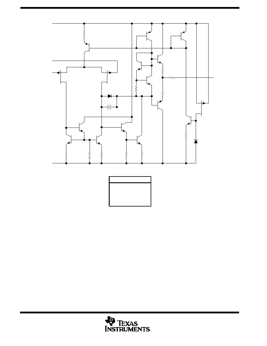
schematic (each amplifier)
C1
VCC +
IN +
VCC ≠
1080
1080
IN ≠
64
128
64
OUT
All component values shown are nominal.
COMPONENT COUNT
Resistors
76
Resistors
Transistors
76
120
JFET
20
Diodes
12
Capacitors
8

SLOS136 ≠ APRIL 1994
3
POST OFFICE BOX 655303
∑
DALLAS, TEXAS 75265
absolute maximum ratings over operating free-air temperature range (unless otherwise noted)
Supply voltage, V
CC+
(see Note 1)
18 V
. . . . . . . . . . . . . . . . . . . . . . . . . . . . . . . . . . . . . . . . . . . . . . . . . . . . . . . . . . .
Supply voltage, V
CC ≠
(see Note 1)
≠18 V
. . . . . . . . . . . . . . . . . . . . . . . . . . . . . . . . . . . . . . . . . . . . . . . . . . . . . . . . . .
Differential input voltage, V
ID
(see Note 2)
±
30 V
. . . . . . . . . . . . . . . . . . . . . . . . . . . . . . . . . . . . . . . . . . . . . . . . . . .
Input voltage, V
I
(any input) (see Notes 1 and 3)
±
15 V
. . . . . . . . . . . . . . . . . . . . . . . . . . . . . . . . . . . . . . . . . . . . . .
Duration of output short circuit to ground (see Note 4)
unlimited
. . . . . . . . . . . . . . . . . . . . . . . . . . . . . . . . . . . . . .
Continuous total dissipation
See Dissipation Rating Table
. . . . . . . . . . . . . . . . . . . . . . . . . . . . . . . . . . . . . . . . . . . .
Operating free-air temperature range, T
A
0
∞
C to 70
∞
C
. . . . . . . . . . . . . . . . . . . . . . . . . . . . . . . . . . . . . . . . . . . . . .
Storage temperature range
≠ 65
∞
C to 150
∞
C
. . . . . . . . . . . . . . . . . . . . . . . . . . . . . . . . . . . . . . . . . . . . . . . . . . . . . . . .
Lead temperature 1,6 mm (1/16 inch) from case for 10 seconds
260
∞
C
. . . . . . . . . . . . . . . . . . . . . . . . . . . . . . . .
Stresses beyond those listed under "absolute maximum ratings" may cause permanent damage to the device. These are stress ratings only, and
functional operation of the device at these conditions is not implied. Exposure to absolute-maximum-rated conditions for extended periods may
affect device reliability.
NOTES:
1. All voltage values, except differential voltages and VCC specified for the measurement of IOS, are with respect to the midpoint
between VCC + and VCC ≠ .
2. Differential voltages are at IN + with respect to IN ≠.
3. The magnitude of the input voltage must never exceed the magnitude of the supply voltage or 15 V, whichever is less.
4. The output can be shorted to ground or to either supply. Temperature and/or supply voltages must be limited to ensure that the
dissipation rating is not exceeded.
DISSIPATION RATING TABLE
PACKAGE
TA
25
∞
C
POWER RATING
DERATING FACTOR
ABOVE TA = 25
∞
C
TA = 70
∞
C
POWER RATING
DB
1024 mW
8.2 mW/
∞
C
655 mW

SLOS136 ≠ APRIL 1994
4
POST OFFICE BOX 655303
∑
DALLAS, TEXAS 75265
electrical characteristics, V
CC
±
=
±
15 V (unless otherwise noted)
PARAMETER
TEST CONDITIONS
TA
MIN
TYP
MAX
UNIT
VIO
Input offset voltage
VO = 0
RS = 50
25
∞
C
5
15
mV
VIO
Input offset voltage
VO = 0,
RS = 50
Full range
20
mV
VIO
Temperature coefficient of input offset
voltage
VO = 0,
RS = 50
Full range
10
µ
V/
∞
C
IIO
Input offset current
VO = 0
25
∞
C
5
200
pA
IIO
Input offset current
VO = 0
Full range
5
nA
IIB
Inp t bias c rrentß
VO = 0
25
∞
C
30
400
pA
IIB
Input bias currentß
VO = 0
Full range
10
nA
VICR
Common-mode input voltage range
25
∞
C
±
10
±
11
V
RL = 10 k
25
∞
C
±
12
±
13.5
VOM
Maximum peak output voltage swing
RL
10 k
Full range
±
12
V
RL
2 k
Full range
±
10
±
12
AVD
Large-signal differential voltage
VO =
±
10 V,
RL
2 k
25
∞
C
25
200
V/mV
AVD
g
g
g
amplification
VO =
±
10 V,
RL
2 k
Full range
15
V/mV
B1
Unity-gain bandwidth
25
∞
C
3
MHz
ri
Input resistance
25
∞
C
1012
CMRR
Common mode rejection ratio
VIC = VICRmin,
VO = 0,
25
∞
C
70
76
dB
CMRR
Common-mode rejection ratio
IC
ICR
,
RS = 50
O
,
25
∞
C
70
76
dB
kSVR
Supply-voltage rejection ratio
VCC =
±
15 V to
±
9 V,
VO = 0,
25
∞
C
70
76
dB
kSVR
y
g
j
(
VCC
±
/
VIO)
CC
,
RS = 50
O
,
25
∞
C
70
76
dB
ICC
Supply current (per amplifier)
VO = 0,
No load
25
∞
C
1.4
2.8
mA
VO1/VO2 Crosstalk attenuation
AVD = 100
25
∞
C
120
dB
All characteristics are measured under open-loop conditions with zero common-mode voltage unless otherwise specified.
Full range is 0
∞
C to 70
∞
C.
ß Input bias currents of a FET-input operational amplifier are normal junction reverse currents, which are temperature sensitive as shown in
Figure 14. Pulse techniques must be used that will maintain the junction temperature as close to the ambient temperature as possible.
operating characteristics, V
CC
±
=
±
15 V, T
A
= 25
∞
C (unless otherwise noted)
PARAMETER
TEST CONDITIONS
MIN
TYP
MAX
UNIT
SR
Slew rate at unity gain
VI = 10 V,
RL = 2 k
,
CL = 100 pF, See Figure 1
13
V/
µ
s
tr
Rise time
VI = 20 mV
RL = 2 k
CL = 100 pF
See Figure 1
0.05
µ
s
Overshoot factor
VI = 20 mV,
RL = 2 k
,
CL = 100 pF, See Figure 1
20%
Vn
Equivalent input noise voltage
RS = 20
,
f = 1 kHz
18
nV/
Hz

SLOS136 ≠ APRIL 1994
5
POST OFFICE BOX 655303
∑
DALLAS, TEXAS 75265
PARAMETER MEASUREMENT INFORMATION
Figure 1. Unity-Gain Amplifier
VI
CL = 100 pF
RL = 2 k
+
≠
OUT
Figure 2. Gain-of-10 Inverting Amplifier
VI
10 k
1 k
RL
CL = 100 pF
+
≠
OUT
TYPICAL CHARACTERISTICS
Table of Graphs
FIGURE
vs Frequency
3, 4, 5
VOM
Maximum peak output voltage
vs Frequency
vs Free-air temperature
3, 4, 5
6
VOM
Maximum peak output voltage
vs Load resistance
7
vs Supply voltage
8
AVD
Large signal differential voltage amplification
vs Free-air temperature
9
AVD
Large-signal differential voltage amplification
vs Frequency
10
PD
Total power dissipation
vs Free-air temperature
11
ICC
Supply current
vs Free-air temperature
12
ICC
Supply current
vs Supply voltage
13
IIB
Input bias current
vs Free-air temperature
14
Pulse response
Large signal
15
VO
Output voltage
vs Elasped time
16
CMRR
Common-mode rejection ratio
vs Free-air temperature
17
Vn
Equivalent input noise voltage
vs Frequency
18
THD
Total harmonic distortion
vs Frequency
19
Phase shift
vs Free-air temperature
10