
TL2218-285, TL2218-285Y
EXCALIBUR CURRENT-MODE SCSI TERMINATOR
SLVS072C ≠ DECEMBER 1992 ≠ REVISED OCTOBER 1995
POST OFFICE BOX 655303
∑
DALLAS, TEXAS 75265
Copyright
©
1995, Texas Instruments Incorporated
8≠1
available features
∑
Fully Integrated 9-Channel SCSI
Termination
∑
No External Components Required
∑
Maximum Allowed Current Applied at First
High-Level Step
∑
6-pF Typical Power-Down Output
Capacitance
∑
Wide V
term
(Termination Voltage)
Operating Range, 3.5 V to 5.5 V
∑
TTL-Compatible Disable Feature
∑
Compatible With Active Negation
∑
Thermal Regulation
description
The TL2218-285 is a current-mode 9-channel monolithic terminator specially designed for single-ended
small-computer-systems-interface (SCSI) bus termination. A user-controlled disable function is provided to
reduce standby power. No impedance-matching resistors or other external components are required for its
operation as a complete terminator.
The device operates over a wide termination-voltage (V
term
) range of 3.5 V to 5.5 V, offering an extra 0.5 V of
operating range when compared to the minimum termination voltage of 4 V required by other integrated active
terminators. The TL2218-285 functions as a current-sourcing terminator and supplies a constant output current
of 23 mA into each asserted line. When a line is deasserted, the device senses the rising voltage level and begins
to function as a voltage source, supplying a fixed output voltage of 2.85 V. The TL2218-285 features
compatibility with active negation drivers and has a typical sink current capability of 20 mA.
The TL2218-285 is able to ensure that maximum current is applied at the first high-level step. This performance
means that the device should provide a first high-level step exceeding 2 V even at a 10-MHz rate. Therefore,
noise margins are improved considerably above those provided by resistive terminators.
A key difference between the TL2218-285 current-mode terminator and a Boulay terminator is that the
TL2218-285 does not incorporate a low dropout regulator to set the output voltage to 2.85 V. In contrast with
the Boulay termination concept, the accuracy of the 2.85 V is not critical with the current-mode method used
in the TL2218-285 because this voltage does not determine the driver current. Therefore, the primary device
specifications are not the same as with a voltage regulator but are more concerned with output current.
The DISABLE terminal is TTL compatible and must be taken low to shut down the outputs. The device is
normally active, even when DISABLE is left floating. In the disable mode, only the device startup circuits remain
active, thereby reducing the supply current to just 500
µ
A. Output capacitance in the shutdown mode is typically
6 pF.
The TL2218-285 has on-board thermal regulation and current limiting, thus eliminating the need for external
protection circuitry. A thermal regulation circuit that is designed to provide current limiting, rather than an actual
thermal shutdown, is included in the individual channels of the TL2218-285. When a system fault occurs that
leads to excessive power dissipation by the terminator, the thermal regulation circuit causes a reduction in the
asserted-line output current sufficient to maintain operation. This feature allows the bus to remain active during
a fault condition, which permits data transfer immediately upon removal of the fault. A terminator with thermal
shutdown does not allow for data transfer until sufficient cooling has occurred. Another advantage offered by
the TL2218-285 is a design that does not require costly laser trimming in the manufacturing process.
The TL2218-285 is characterized for operation over the virtual junction temperature range of 0
∞
C to 125
∞
C.
This symbol is not presently listed within EIA/JEDEC standards for letter symbols.
2
3
4
5
6
7
8
9
10
20
19
18
17
16
15
14
13
12
11
TERMPWR
NC
NC
D0
D1
D2
D3
D4
NC
GND
TERMPWR
DISABLE
NC
D8
D7
NC
D6
D5
NC
GND
PW PACKAGE
(TOP VIEW)
1
NC ≠ No internal connection
PRODUCTION DATA information is current as of publication date.
Products conform to specifications per the terms of Texas Instruments
standard warranty. Production processing does not necessarily include
testing of all parameters.

TL2218-285, TL2218-285Y
EXCALIBUR CURRENT-MODE SCSI TERMINATOR
SLVS072C ≠ DECEMBER 1992 ≠ REVISED OCTOBER 1995
POST OFFICE BOX 655303
∑
DALLAS, TEXAS 75265
8≠2
AVAILABLE OPTIONS
TJ
SURFACE MOUNT
(PW)
CHIP FORM
(Y)
0
∞
C to 125
∞
C
TL2218-285PWLE
TL2218-285Y
The PW package is only available left-end taped and reeled.
TL2218-285Y chip information
This chip, when properly assembled, displays characteristics similar to the TL2218-285. Thermal compression
or ultrasonic bonding may be used on the doped aluminum bonding pads. The chip may be mounted with
conductive epoxy or a gold-silicon preform.
BONDING PAD ASSIGNMENTS
CHIP THICKNESS: 11 MILS TYPICAL
BONDING PADS: 4
◊
4 MILS MINIMUM
TJmax = 150
∞
C
TOLERANCES ARE
±
10%.
ALL DIMENSIONS ARE IN MILS.
Thermal
Regulation
Feedback
Active
Negation
Clamp
TERMPWR
1, 20
4
19
Vref
DISABLE
D0
Common to All Channels
161
84
(1)
(4)
(5)
(6)
(7)
(8)
(10) (11)
(13)
(14)
(16)
(17)
(19)
(20)

TL2218-285, TL2218-285Y
EXCALIBUR CURRENT-MODE SCSI TERMINATOR
SLVS072C ≠ DECEMBER 1992 ≠ REVISED OCTOBER 1995
POST OFFICE BOX 655303
∑
DALLAS, TEXAS 75265
8≠3
functional block diagram (each channel)
Thermal
Regulation
Feedback
Active
Negation
Clamp
TERMPWR
1, 20
4
19
Vref
DISABLE
D0
Common to All Channels
absolute maximum ratings over operating free-air temperature range (unless otherwise noted)
(see Figures 1, 2, and 3)
Continuous termination voltage
10 V
. . . . . . . . . . . . . . . . . . . . . . . . . . . . . . . . . . . . . . . . . . . . . . . . . . . . . . . . . . . . .
Continuous output voltage range
0 V to 5.5 V
. . . . . . . . . . . . . . . . . . . . . . . . . . . . . . . . . . . . . . . . . . . . . . . . . . . . . .
Continuous disable voltage range
0 V to 5.5 V
. . . . . . . . . . . . . . . . . . . . . . . . . . . . . . . . . . . . . . . . . . . . . . . . . . . . .
Continuous total power dissipation
See Dissipation Rating Table
. . . . . . . . . . . . . . . . . . . . . . . . . . . . . . . . . . . . .
Operating virtual junction temperature range, T
J
≠ 55
∞
C to 150
∞
C
. . . . . . . . . . . . . . . . . . . . . . . . . . . . . . . . . . . .
Storage temperature range, T
stg
≠ 60
∞
C to 150
∞
C
. . . . . . . . . . . . . . . . . . . . . . . . . . . . . . . . . . . . . . . . . . . . . . . . . .
Lead temperature 1,6 mm (1/16 inch) from case for 10 seconds
260
∞
C
. . . . . . . . . . . . . . . . . . . . . . . . . . . . . . .
Stresses beyond those listed under "absolute maximum ratings" may cause permanent damage to the device. These are stress ratings only, and
functional operation of the device at these or any other conditions beyond those indicated under "recommended operating conditions" is not
implied. Exposure to absolute-maximum-rated conditions for extended periods may affect device reliability.
DISSIPATION RATING TABLE
PACKAGE
POWER RATING
T
25
∞
C
DERATING FACTOR
T = 70
∞
C
T = 85
∞
C
T = 125
∞
C
PACKAGE
AT
POWER RATING
ABOVE T = 25
∞
C
POWER RATING
POWER RATING
POWER RATING
TA
828 mW
6.62 mW/
∞
C
530 mW
430 mW
166 mW
PW
TC
4032 mW
32.2 mW/
∞
C
2583 mW
2100 mW
812 mW
TL
2475 mW
19.8 mW/
∞
C
1584 mW
1287 mW
495 mW
R
JL is the thermal resistance between the junction and device lead. To determine the virtual junction temperature (TJ) relative to the device lead
temperature, the following calculations should be used: TJ = PD x R
JL + TL , where PD is the internal power dissipation of the device and TL is
the device lead temperature at the point of contact to the printed wiring board. R
JL is 50.5
∞
C/W.
TL2218-285, TL2218-285Y
EXCALIBUR CURRENT-MODE SCSI TERMINATOR
SLVS072C ≠ DECEMBER 1992 ≠ REVISED OCTOBER 1995
POST OFFICE BOX 655303
∑
DALLAS, TEXAS 75265
8≠4
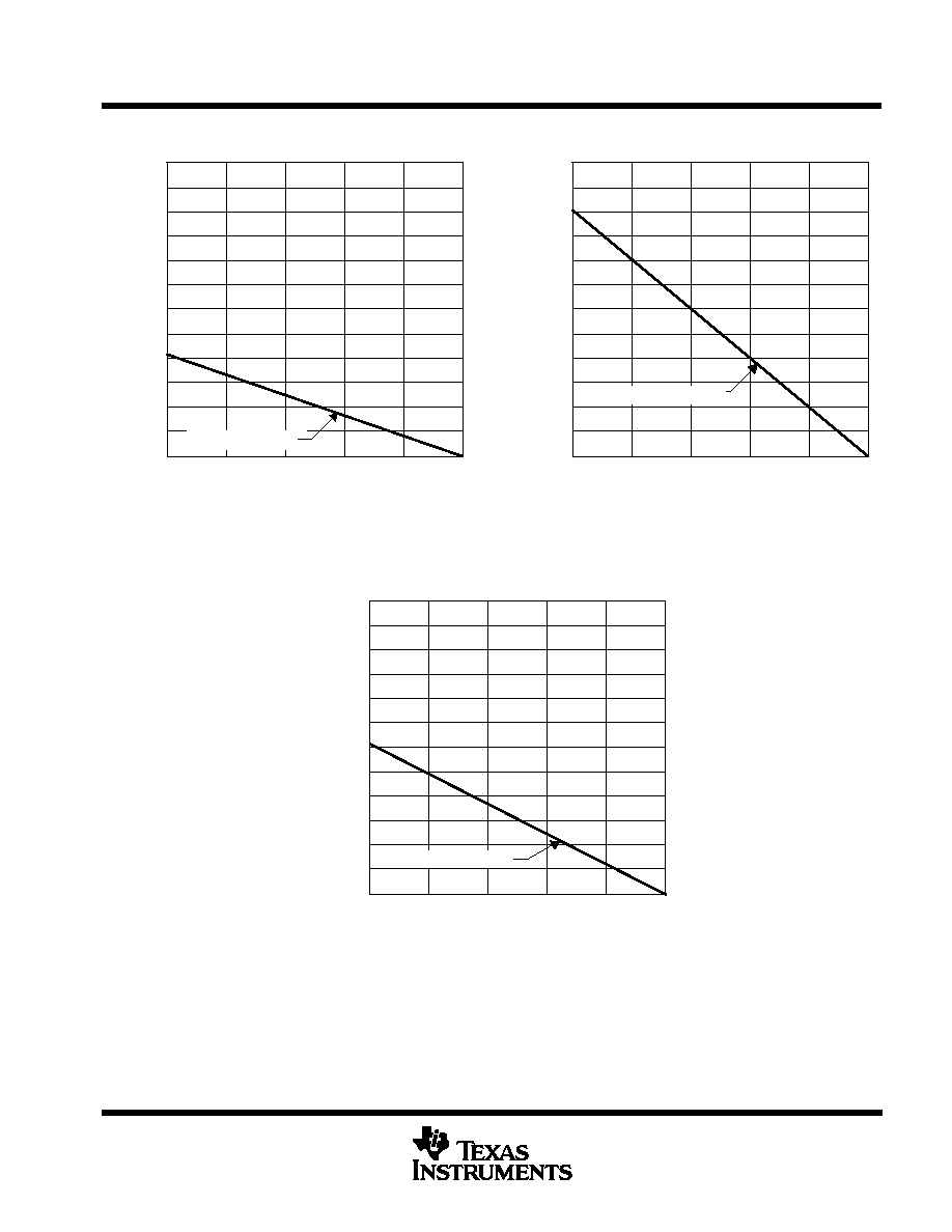
600
400
200
0
25
50
75
100
800
1000
1200
125
150
1800
1600
1400
2000
2200
2400
FREE-AIR TEMPERATURE
DISSIPATION DERATING CURVE
TA ≠ Free-Air Temperature ≠
∞
C
Maximum Continuous Power Dissipation ≠ mW
1200
800
400
0
25
50
75
100
1600
2000
2400
125
150
3600
3200
2800
4000
4400
4800
CASE TEMPERATURE
DISSIPATION DERATING CURVE
TC ≠ Case Temperature ≠
∞
C
R
JA = 151
∞
C/W
R
JC = 31
∞
C/W
Maximum Continuous Power Dissipation ≠ mW
Figure 1
Figure 2
1200
800
400
0
25
50
75
100
2000
125
150
3600
3200
2800
4000
4400
4800
LEAD TEMPERATURE
DISSIPATION DERATING CURVE
TL ≠ Lead Temperature ≠
∞
C
2400
1600
R
JL = 50.5
∞
C/W
Maximum Continuous Power Dissipation ≠ mW
Figure 3
R
JL is the thermal resistance between the junction and device lead. To determine the virtual junction temperature (TJ) relative to the device lead
temperature, the following calculations should be used: TJ = PD x R
JL + TL, where PD is the internal power dissipation of the device, and TL is
the device lead temperature at the point of contact to the printed wiring board. R
JL is 50.5
∞
C/W.

TL2218-285, TL2218-285Y
EXCALIBUR CURRENT-MODE SCSI TERMINATOR
SLVS072C ≠ DECEMBER 1992 ≠ REVISED OCTOBER 1995
POST OFFICE BOX 655303
∑
DALLAS, TEXAS 75265
8≠5
recommended operating conditions
MIN
MAX
UNIT
Termination voltage
3.5
5.5
V
High-level disable input voltage, VIH
2
Vterm
V
Low-level disable input voltage, VIL
0
0.8
V
Operating virtual junction temperature, TJ
0
125
∞
C
electrical characteristics, V
term
= 4.75 V, V
O
= 0.5 V, T
J
= 25
∞
C
PARAMETER
TEST CONDITIONS
MIN
TYP
MAX
UNIT
Output high voltage
2.5
2.85
V
All data lines open
9
mA
TERMPWR supply current
All data lines = 0.5 V
228
mA
DISABLE = 0 V
500
µ
A
Output current
≠ 20.5
≠ 23
≠ 24
mA
Disable input current (see Note 1)
DISABLE = 4.75 V
1
µ
A
Disable input current (see Note 1)
DISABLE = 0 V
600
µ
A
Output leakage current
DISABLE = 0 V
100
nA
Output capacitance, device disabled
VO = 0 V,
1 MHz
6
pF
Termination sink current, total
VO = 4 V
20
mA
NOTE 1: When DISABLE is open or high, the terminator is active.