 | –≠–ª–µ–∫—Ç—Ä–æ–Ω–Ω—ã–π –∫–æ–º–ø–æ–Ω–µ–Ω—Ç: TL343 | –°–∫–∞—á–∞—Ç—å:  PDF PDF  ZIP ZIP |

TL343
SINGLE LOW-POWER OPERATIONAL AMPLIFIER
SLOS250D ≠ JUNE 1999 ≠ REVISED NOVEMBER 1999
1
POST OFFICE BOX 655303
∑
DALLAS, TEXAS 75265
D
Wide Range of Supply Voltages, Single
Supply 5 V to 30 V, or Dual Supplies
D
Class AB Output Stage
D
True Differential-Input Stage
D
Low Input Bias Current
D
Internal Frequency Compensation
D
Short-Circuit Protection
D
Packaged in SOT-23 Package
description
The TL343 is a single operational amplifier similar in performance to the
µ
A741, but with several distinct
advantages. It is designed to operate from a single supply over a range of voltages from 3 V to 36 V. Operation
from split supplies also is possible, provided the difference between the two supplies is 3 V to 36 V. The
common-mode input range includes the negative supply. Output range is from the negative supply to
V
CC
≠ 1.5 V.
The TL343 is characterized for operation from ≠40
∞
C to 125
∞
C.
symbol
≠
+
IN+
OUT
IN≠
AVAILABLE OPTIONS
TA
VIOMAX
AT 25
∞
C
SOT-23
PACKAGE
(DBV)
≠40
∞
C to 125
∞
C
10 mV
TL343IDBV
The DBV package is only available taped and
reeled. Add the suffix R to device type for ordering
(e.g., TL343IDBVR).
Copyright
©
1999, Texas Instruments Incorporated
PRODUCTION DATA information is current as of publication date.
Products conform to specifications per the terms of Texas Instruments
standard warranty. Production processing does not necessarily include
testing of all parameters.
Please be aware that an important notice concerning availability, standard warranty, and use in critical applications of
Texas Instruments semiconductor products and disclaimers thereto appears at the end of this data sheet.
DBV PACKAGE
(TOP VIEW)
1
2
3
5
4
IN+
V
CC≠
/GND
IN≠
V
CC
+
OUT
TL343
SINGLE LOW-POWER OPERATIONAL AMPLIFIER
SLOS250D ≠ JUNE 1999 ≠ REVISED NOVEMBER 1999
2
POST OFFICE BOX 655303
∑
DALLAS, TEXAS 75265
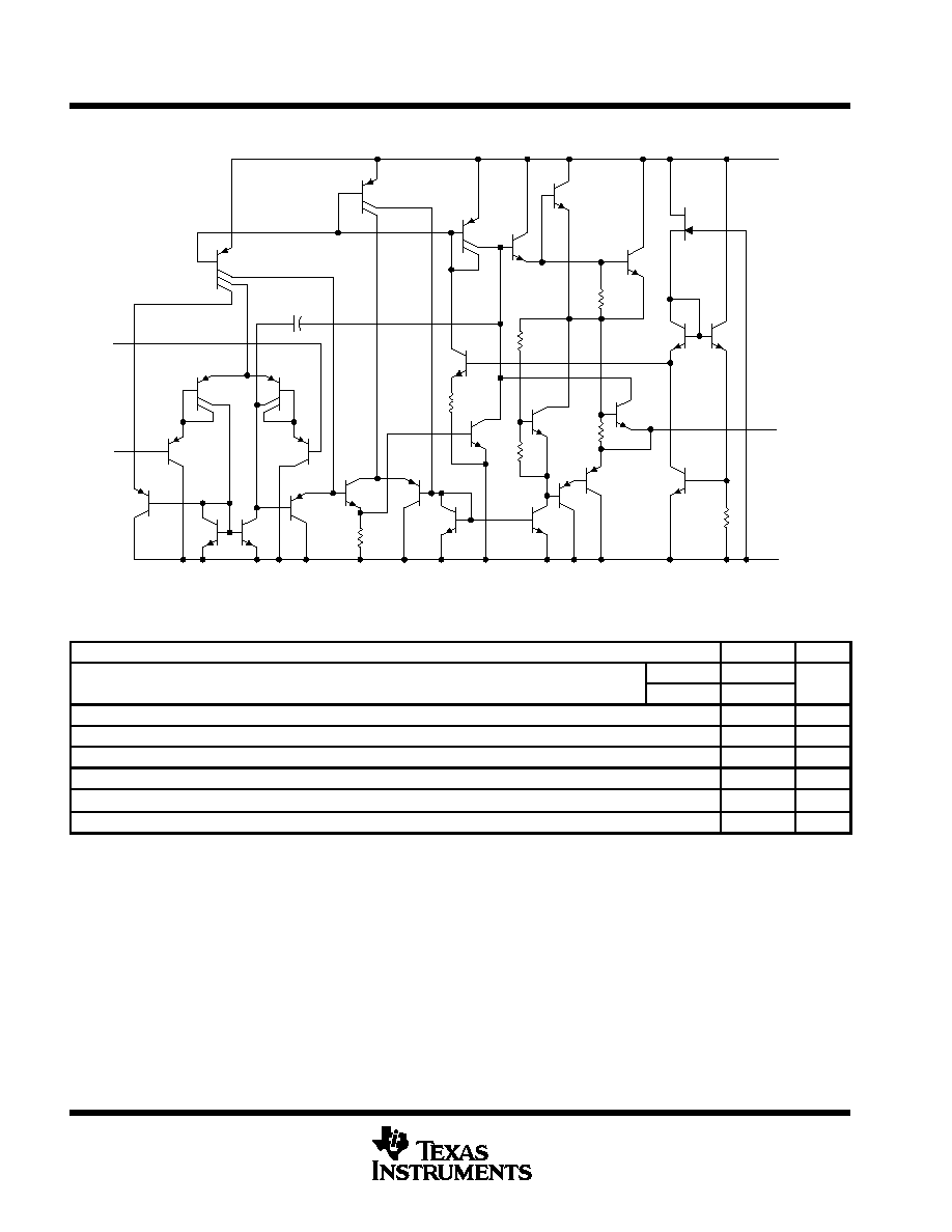
schematic
IN≠
IN+
VCC+
VCC≠/GND
OUT
2.4 k
5 pF
NOTE A: Component values shown are nominal.
absolute maximum ratings over operating free-air temperature range (unless otherwise noted)
MAX
UNIT
Supply voltage (see Note 1)
VCC+
18
V
Supply voltage (see Note 1)
VCC≠
≠18
V
Supply voltage, VCC+ with respect to VCC≠
36
V
Differential input voltage (see Note 2)
±
36
V
Input voltage (see Notes 1 and 3)
±
18
V
Package thermal impedance,
JA (see Note 4)
347
∞
C/W
Lead temperature 1,6 mm (1/16 inch) from case for 10 seconds
260
∞
C
Storage temperature range, Tstg
≠65 to 150
∞
C
NOTES:
1. These voltage values are with respect to the midpoint between VCC+ and VCC≠.
2. Differential voltages are at IN+ with respect to IN≠.
3. Neither input must ever be more positive than VCC+ or more negative than VCC≠.
4. The package thermal impedance is calculated in accordance with JESD 51.
TL343
SINGLE LOW-POWER OPERATIONAL AMPLIFIER
SLOS250D ≠ JUNE 1999 ≠ REVISED NOVEMBER 1999
3
POST OFFICE BOX 655303
∑
DALLAS, TEXAS 75265
recommended operating conditions
MIN
MAX
UNIT
Single-supply voltage
VCC
5
30
V
Dual supply voltage
VCC+
2.5
15
V
Dual-supply voltage
VCC≠
≠2.5
≠15
V
Operating free-air temperature, TA
≠40
125
∞
C
electrical characteristics at specified free-air temperature, V
CC
±
=
±
15 V (unless otherwise noted)
PARAMETER
TEST CONDITIONS
MIN
TYP
MAX
UNIT
VIO
Input offset voltage
See Note 5
25
∞
C
2
10
mV
VIO
Input offset voltage
See Note 5
Full range
12
mV
a
V
IO
Temperature coefficient
of input offset voltage
See Note 5
Full range
10
µ
V/
∞
C
IIO
Input offset current
See Note 5
25
∞
C
30
50
nA
IIO
Input offset current
See Note 5
Full range
200
nA
a
I
IO
Temperature coefficient
of input offset current
See Note 5
Full range
50
pA/C
IIB
Input bias current
See Note 5
25
∞
C
≠20
≠50
nA
IIB
Input bias current
See Note 5
Full range
≠80
nA
VICR
Common-mode input voltage range
25
∞
C
VCC≠
to 13
VCC≠
to 13.5
V
RL = 10 k
25
∞
C
±
12
±
13.5
VOM
Peak output-voltage swing
RL = 2 k
25
∞
C
±
10
±
13
V
RL = 2 k
Full range
±
10
AVD
Large-signal differential
VO =
±
10 V
RL = 2 k
25
∞
C
20
200
V/mV
AVD
g
g
voltage amplification
VO =
±
10 V,
RL = 2 k
Full range
15
V/mV
BOM
Maximum-output-swing bandwidth
VOPP = 20 V,
THD
5%,
AVD = 1,
RL = 2 k
25
∞
C
9
kHz
B1
Unity-gain bandwidth
VO = 50 mV,
RL = 10 k
25
∞
C
1
MHz
m
Phase margin
CL = 200 pF,
RL = 2 k
25
∞
C
44
∞
ri
Input resistance
f = 20 Hz
25
∞
C
0.3
1
M
ro
Output resistance
f = 20 Hz
25
∞
C
75
CMRR
Common-mode rejection ratio
VIC = VICR(min)
25
∞
C
70
90
dB
kSVS
Supply-voltage sensitivity (
VIO/
VCC)
VCC
±
=
±
2.5 to
±
15 V
25
∞
C
30
150
µ
V/V
IOS
Short-circuit output currentß
25
∞
C
±
10
±
30
±
55
mA
ICC
Total supply current
No load,
See Note 5
25
∞
C
0.7
2.8
mA
All characteristics are measured under open-loop conditions with zero common-mode voltage unless otherwise specified. Full range for TA is
≠40
∞
C to 125
∞
C.
The VICR limits are linked directly, volt-for-volt, to supply voltage; the positive limit is 2 V less than VCC+.
ß Temperature and/or supply voltages must be limited to ensure that the dissipation rating is not exceeded.
NOTE 5: VIO, IIO, IIB, and ICC are defined at VO = 0.
TL343
SINGLE LOW-POWER OPERATIONAL AMPLIFIER
SLOS250D ≠ JUNE 1999 ≠ REVISED NOVEMBER 1999
4
POST OFFICE BOX 655303
∑
DALLAS, TEXAS 75265
electrical characteristics, V
CC+
= 5 V, V
CC≠
= 0 V, T
A
= 25
∞
C (unless otherwise noted)
PARAMETER
TEST CONDITIONS
MIN
TYP
MAX
UNIT
VIO
Input offset voltage
VO = 2.5 V
2
10
mV
IIO
Input offset current
VO = 2.5 V
30
50
nA
IIB
Input bias current
VO = 2.5 V
≠20
≠50
nA
VOM
Peak output voltage swing
RL = 10 k
3.3
3.5
V
AVD
Large-signal differential voltage
amplification
VO = 1.7 V to 3.3 V,
RL = 2 k
20
200
V/mV
kSVS
Supply-voltage sensitivity (
VIO/
VCC
±
)
VCC
±
=
±
2.5 V to
±
15 V
150
µ
V/V
ICC
Supply current
VO = 2.5 V,
No load
0.7
1.75
mA
All characteristics are measured under open-loop conditions with zero common-mode input voltage unless otherwise specified.
Output swings essentially to ground.
operating characteristics, V
CC
±
=
±
15 V, T
A
= 25
∞
C, A
VD
= 1 (unless otherwise noted)
PARAMETER
TEST CONDITIONS
MIN
TYP
MAX
UNIT
SR
Slew rate at unity gain
VI =
±
10 V,
CL = 100 pF,
RL = 2 k
,
See Figure 1
1
V/
µ
s
tr
Rise time
VO = 50 mV,
CL = 100 pF,
RL = 10 k
,
See Figure 1
0.35
µ
s
tf
Fall time
VO = 50 mV,
CL = 100 pF,
RL = 10 k
,
See Figure 1
0.35
µ
s
Overshoot factor
VO = 50 mV,
CL = 100 pF,
RL = 10 k
,
See Figure 1
20%
Crossover distortion
VI(PP) = 30 mV,
VOPP = 2 V,
f = 10 kH
Z
1%
PARAMETER MEASUREMENT INFORMATION
+
≠
RL
CL = 100 pF
VI
OUT
Figure 1. Unity-Gain Amplifier

TL343
SINGLE LOW-POWER OPERATIONAL AMPLIFIER
SLOS250D ≠ JUNE 1999 ≠ REVISED NOVEMBER 1999
5
POST OFFICE BOX 655303
∑
DALLAS, TEXAS 75265
TYPICAL CHARACTERISTICS
0
≠75
I
TA ≠ Free-Air Temperature ≠
∞
C
50
100
150
200
250
≠50
≠25
0
25
50
75
100
125
VCC
±
=
±
15 V
INPUT BIAS CURRENT
vs
FREE-AIR TEMPERATURE
Figure 2
IB
≠ Input Bias Current ≠ nA
|VCC
±
| ≠ Supply Voltage ≠ V
0
250
200
150
100
50
0
2
4
8
10
12
14
16
6
TA = 25
∞
C
INPUT BIAS CURRENT
vs
SUPPLY VOLTAGE
Figure 3
I
IB
≠ Input Bias Current ≠ nA
|VCC
±
| ≠ Supply Voltage ≠ V
V
0
0
5
10
15
20
25
30
2
4
6
8
10
12
14
16
RL = 10 k
TA = 25
∞
C
MAXIMUM PEAK-TO-PEAK OUTPUT VOLTAGE
vs
SUPPLY VOLTAGE
Figure 4
OPP
≠ Maximum Peak-to-Peak Output V
oltage ≠ V
1 k
f ≠ Frequency ≠ Hz
30
25
20
15
10
5
0
10 k
100 k
1 M
MAXIMUM PEAK-TO-PEAK OUTPUT VOLTAGE
vs
FREQUENCY
Figure 5
V
OPP
≠ Maximum Peak-to-Peak Output V
oltage ≠ V
ŒŒŒŒŒ
ŒŒŒŒŒ
ŒŒŒŒŒ
ŒŒŒŒŒ
ŒŒŒŒŒ
VCC
±
=
±
15 V
CL = 0
RL = 10 k
TA = 25
∞
C
See Figure 1
Operation of the device at these or any other conditions beyond those indicated under "recommended operating conditions" is not implied.