 | –≠–ª–µ–∫—Ç—Ä–æ–Ω–Ω—ã–π –∫–æ–º–ø–æ–Ω–µ–Ω—Ç: TL3x071 | –°–∫–∞—á–∞—Ç—å:  PDF PDF  ZIP ZIP |
TL3x071, TL3x071A, TL3x072, TL3x072A, TL3x074, TL3x074A
HIGH-SLEW-RATE, SINGLE-SUPPLY OPERATIONAL AMPLIFIERS
SLOS097C ≠ MARCH 1991 ≠ REVISED AUGUST 1996
1
POST OFFICE BOX 655303
∑
DALLAS, TEXAS 75265
D
Wide Gain-Bandwidth Product . . . 4.5 MHz
D
High Slew Rate . . . 13 V/
µ
s
D
Fast Settling Time . . . 1.1
µ
s to 0.1%
D
Wide-Range Single-Supply Operation
4 V to 44 V
D
Wide Input Common-Mode Range Includes
Ground (V
CC ≠
)
D
Low Total Harmonic Distortion . . . 0.02%
D
Low Input Offset Voltage . . . 3 mV Max
(A Suffix)
D
Large Output Voltage Swing
≠ 14.7 V to 14 V (With
±
15-V Supplies)
D
Large Capacitance Drive Capability
10,000 pF
D
Excellent Phase Margin . . . 60
∞
D
Excellent Gain Margin . . . 12 dB
D
Output Short-Circuit Protection
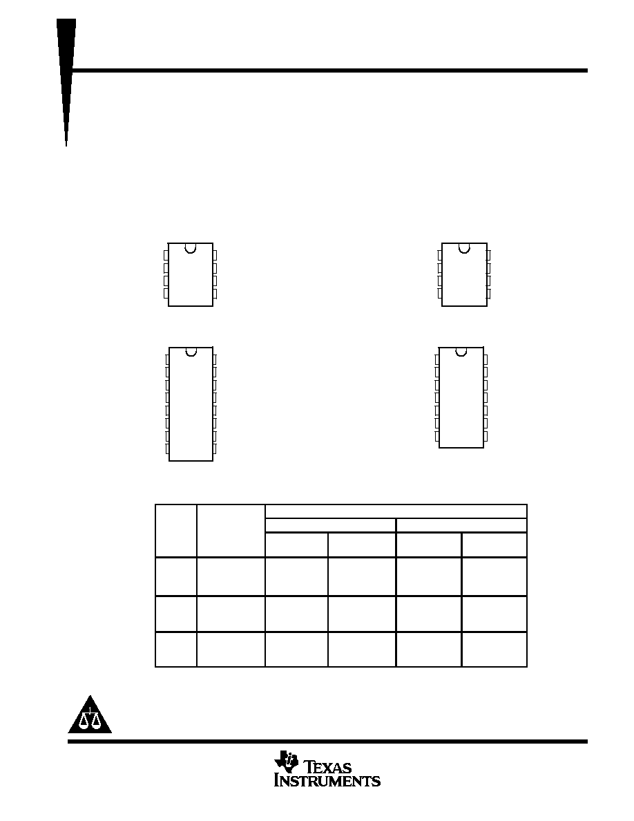
1
2
3
4
8
7
6
5
OFSET N1
IN ≠
IN +
V
CC ≠
/GND
NC
V
CC +
OUT
OFSET N2
D OR P PACKAGE
(SINGLE, TOP VIEW)
NC ≠ No internal connection
1
2
3
4
8
7
6
5
1OUT
1IN ≠
1IN +
V
CC ≠
/GND
V
CC +
2OUT
2IN ≠
2IN +
D OR P PACKAGE
(DUAL, TOP VIEW)
1
2
3
4
5
6
7
8
16
15
14
13
12
11
10
9
1OUT
1IN ≠
1IN +
V
CC +
2IN +
2IN ≠
2OUT
NC
4OUT
4IN ≠
4IN +
V
CC ≠
/GND
3IN +
3IN ≠
3OUT
NC
(QUAD, TOP VIEW)
DW PACKAGE
1
2
3
4
5
6
7
14
13
12
11
10
9
8
1OUT
1IN ≠
1IN +
V
CC +
2IN +
2IN ≠
2OUT
4OUT
4IN ≠
4IN +
V
CC ≠
/GND
3IN +
3IN ≠
3OUT
N PACKAGE
(QUAD, TOP VIEW)
AVAILABLE OPTIONS
PACKAGE
TA
COMPLEXITY
PLASTIC DIP
SMALL OUTLINE
TA
COMPLEXITY
STANDARD
GRADE
PRIME
GRADE
STANDARD
GRADE
PRIME
GRADE
0
∞
C
Single
TL34071P
TL34071AP
TL34071D
TL34071AD
to
Single
Dual
TL34071P
TL34072P
TL34071AP
TL34072AP
TL34071D
TL34072D
TL34071AD
TL34072AD
70
∞
C
Quad
TL34074N
TL34074AN
TL34074DW
TL34074ADW
≠ 40
∞
C
Single
TL33071P
TL33071AP
TL33071D
TL33071AD
40 C
to
g
Dual
TL33072P
TL33072AP
TL33072D
TL33072AD
105
∞
C
Quad
TL33074N
TL33074AN
TL33074DW
TL33074ADW
≠ 55
∞
C
Single
TL35071P
TL35071AP
TL35071D
TL35071AD
55 C
to
g
Dual
TL35072P
TL35072AP
TL35072D
TL35072AD
125
∞
C
Quad
TL35074N
TL35074AN
TL35074DW
TL35074ADW
D and DW packages are available taped and reeled. Add R suffix to device type (e.g., TL34071ADR).
Please be aware that an important notice concerning availability, standard warranty, and use in critical applications of
Texas Instruments semiconductor products and disclaimers thereto appears at the end of this data sheet.
PRODUCTION DATA information is current as of publication date.
Products conform to specifications per the terms of Texas Instruments
standard warranty. Production processing does not necessarily include
testing of all parameters.
Copyright
©
1996, Texas Instruments Incorporated
TL3x071, TL3x071A, TL3x072, TL3x072A, TL3x074, TL3x074A
HIGH-SLEW-RATE, SINGLE-SUPPLY OPERATIONAL AMPLIFIERS
SLOS097C ≠ MARCH 1991 ≠ REVISED AUGUST 1996
2
POST OFFICE BOX 655303
∑
DALLAS, TEXAS 75265
description
Quality, low cost, bipolar fabrication with innovative design concepts are employed for the TL33071/2/4,
TL34071/2/4, and TL35071/2/4 series of monolithic operational amplifiers. This series of operational amplifiers
offers 4.5 MHz of gain bandwidth product, 13 V/
µ
s slew rate, and fast settling time without the use of JFET device
technology. Although this series can be operated from split supplies, it is particularly suited for single-supply
operation since the common-mode input voltage range includes ground potential (V
CC ≠
). With a Darlington
transistor input stage, this series exhibits high input resistance, low input offset voltage, and high gain. The
all-npn output stage, characterized by no dead-band crossover distortion and large output voltage swing,
provides high-capacitance drive capability, excellent phase and gain margins, low open-loop high-frequency
output impedance, and symmetrical source/sink ac frequency response.
The TL34071/2/4 devices are avaliable in standard or prime performance (A-suffix) grades and are specified
over the commercial (0
∞
C to 70
∞
C) temperature range. The TL33071/2/4 devices are available in standard or
prime performance (A-suffix) grades and are specified over industrial/vehicular (≠ 40
∞
C to 105
∞
C) temperature
range. The TL35071/2/4 devices are avaliable in standard or prime performance (A-suffix) grades and are
specified over the military (≠ 55
∞
C to 125
∞
C) temperature range. These low-cost amplifiers are available in
single, dual, and quad configurations and are pin compatible with the MC33071/2/4, MC34071/2/4, and
MC35071/2/4 series of amplifiers. Packaging options include standard plastic DIP and SO packages.
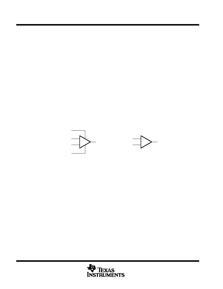
symbol
+
≠
+
≠
OFFSET N1
IN +
IN ≠
OFFSET N2
OUT
Single
OUT
IN +
IN ≠
Dual and Quad
(per amplifier)
TL3x071, TL3x071A, TL3x072, TL3x072A, TL3x074, TL3x074A
HIGH-SLEW-RATE, SINGLE-SUPPLY OPERATIONAL AMPLIFIERS
SLOS097C ≠ MARCH 1991 ≠ REVISED AUGUST 1996
3
POST OFFICE BOX 655303
∑
DALLAS, TEXAS 75265
absolute maximum ratings over operating free-air temperature range (unless otherwise noted)
Supply voltage, V
CC +
(see Note 1)
22 V
. . . . . . . . . . . . . . . . . . . . . . . . . . . . . . . . . . . . . . . . . . . . . . . . . . . . . . . . . . .
Supply voltage, V
CC ≠
≠ 22 V
. . . . . . . . . . . . . . . . . . . . . . . . . . . . . . . . . . . . . . . . . . . . . . . . . . . . . . . . . . . . . . . . . . . . .
Differential input voltage, V
ID
(see Note 2)
±
44 V
. . . . . . . . . . . . . . . . . . . . . . . . . . . . . . . . . . . . . . . . . . . . . . . . . . .
Input voltage, V
I
(any input)
V
CC
±
. . . . . . . . . . . . . . . . . . . . . . . . . . . . . . . . . . . . . . . . . . . . . . . . . . . . . . . . . . . . . . . .
Input current, I
I
(each input)
±
1 mA
. . . . . . . . . . . . . . . . . . . . . . . . . . . . . . . . . . . . . . . . . . . . . . . . . . . . . . . . . . . . . . .
Output current, I
O
±
80 mA
. . . . . . . . . . . . . . . . . . . . . . . . . . . . . . . . . . . . . . . . . . . . . . . . . . . . . . . . . . . . . . . . . . . . . . .
Total current into V
CC +
80 mA
. . . . . . . . . . . . . . . . . . . . . . . . . . . . . . . . . . . . . . . . . . . . . . . . . . . . . . . . . . . . . . . . . . .
Total current out of V
CC ≠
80 mA
. . . . . . . . . . . . . . . . . . . . . . . . . . . . . . . . . . . . . . . . . . . . . . . . . . . . . . . . . . . . . . . . .
Duration of short-circuit current at (or below) 25
∞
C (see Note 3)
unlimited
. . . . . . . . . . . . . . . . . . . . . . . . . . . . . .
Continuous total power dissipation
See Dissipation Rating Table
. . . . . . . . . . . . . . . . . . . . . . . . . . . . . . . . . . . . .
Operating free-air temperature range, T
A
: TL3307x ≠ 40
∞
C to 105
∞
C
. . . . . . . . . . . . . . . . . . . . . . . . . . . . . . . . . . .
TL3407x 0
∞
C to 70
∞
C
. . . . . . . . . . . . . . . . . . . . . . . . . . . . . . . . . . . . . .
TL3507x ≠ 55
∞
C to 125
∞
C
. . . . . . . . . . . . . . . . . . . . . . . . . . . . . . . . . . .
Storage temperature range, T
stg
≠ 65
∞
C to 150
∞
C
. . . . . . . . . . . . . . . . . . . . . . . . . . . . . . . . . . . . . . . . . . . . . . . . . . .
Lead temperature 1.6 mm (1/16 inch) from case for 10 seconds: D, DW, N, or P package
260
∞
C
. . . . . . . . .
Stresses beyond those listed under "absolute maximum ratings" may cause permanent damage to the device. These are stress ratings only, and
functional operation of the device at these or any other conditions beyond those indicated under "recommended operating conditions" is not
implied. Exposure to absolute-maximum-rated conditions for extended periods may affect device reliability.
NOTES:
1. All voltage values, except differential voltages, are with respect to the midpoint between VCC+ and VCC ≠.
2. Differential voltages are at the noninverting input with respect to the inverting input. Excessive current flows if input is brought below
VCC ≠ ≠ 0.3 V.
3. The output can be shorted to either supply. Temperature and/or supply voltages must be limited to ensure that the maximum
dissipation rating is not exceeded.
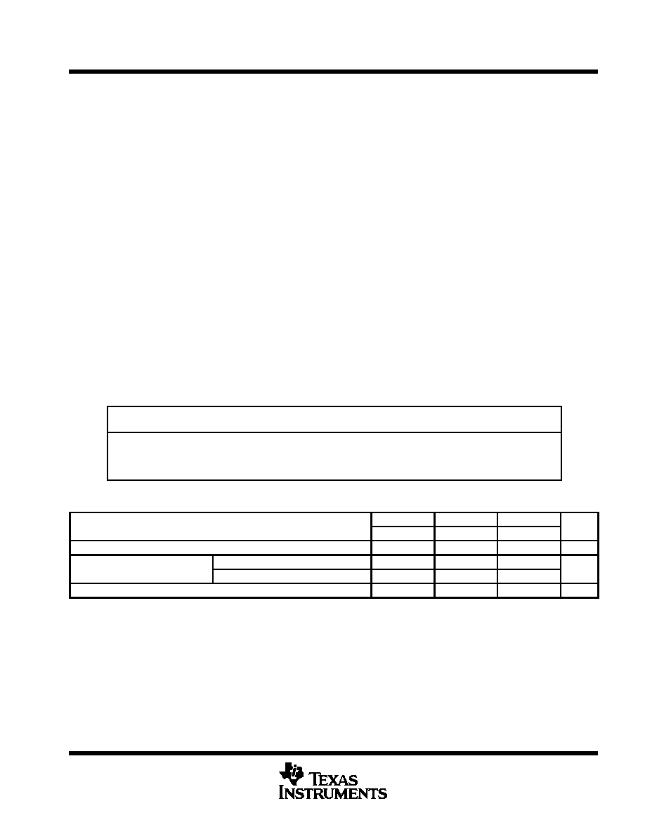
DISSIPATION RATING TABLE
PACKAGE
TA
25
∞
C
DERATING FACTOR
TA = 70
∞
C
TA = 105
∞
C
TA = 125
∞
C
PACKAGE
A
POWER RATING
ABOVE TA = 25
∞
C
A
POWER RATING
A
POWER RATING
A
POWER RATING
D
725 mW
5.8 mW/
∞
C
464 mW
261 mW
145 mW
DW
1025 mW
8.2 mW/
∞
C
656 mW
369 mW
205 mW
N
1150 mW
9.2 mW/
∞
C
736 mW
414 mW
230 mW
P
1000 mW
8.0 mW/
∞
C
640 mW
360 mW
200 mW
recommended operating conditions
TL3307x
TL3407x
TL3507x
UNIT
MIN
MAX
MIN
MAX
MIN
MAX
UNIT
Supply voltage, VCC
±
±
2
±
22
±
2
±
22
±
2
±
22
V
Common mode input voltage VIC
VCC = 5 V
0
2.7
0
2.9
0
2.7
V
Common-mode input voltage, VIC
VCC
±
=
±
15 V
≠ 15
12.7
≠ 15
12.9
≠ 15
12.7
V
Operating free-air temperature, TA
≠ 40
105
0
70
≠ 55
125
∞
C

TL3x071, TL3x071A, TL3x072, TL3x072A, TL3x074, TL3x074A
HIGH-SLEW-RATE, SINGLE-SUPPLY OPERATIONAL AMPLIFIERS
SLOS097C ≠ MARCH 1991 ≠ REVISED AUGUST 1996
4
POST OFFICE BOX 655303
∑
DALLAS, TEXAS 75265
electrical characteristics at specified free-air temperature, V
CC
±
=
±
15 V (unless otherwise noted)
PARAMETER
TEST CONDITIONS
T
TL3x07xA
TL3x07x
PARAMETER
TEST CONDITIONS
TA
MIN
TYP
MAX
MIN
TYP
MAX
UNIT
VCC = 5 V
25
∞
C
0.5
3
1.5
5
VIO
Input offset voltage
VCC =
±
15 V
25
∞
C
0.5
3
1.0
5
mV
VCC =
±
15 V
Full range
5
7
VIO
Temperature coefficient
of input offset voltage
VIC = 0,
V
0
VCC =
±
15 V
Full range
10
10
µ
V/
∞
C
IIO
Input offset current
VO = 0,
RS = 50
VCC =
±
15 V
25
∞
C
7
100
7
100
nA
IIO
Input offset current
RS = 50
VCC =
±
15 V
Full range
250
250
nA
VCC = 5 V
25
∞
C
≠ 0.8
≠ 2
≠ 0.8
≠ 2
IIB
Input bias current
VCC = 5 V
Full range
≠ 2.3
≠ 2.3
µ
A
IIB
Input bias current
VCC =
±
15 V
25
∞
C
≠ 0.7
≠ 1.5
≠ 0.7
≠ 1.5
µ
A
VCC =
±
15 V
Full range
≠ 1.8
≠ 1.8
VICR
Common-mode input
RS = 50
25
∞
C
≠ 15
to
13.2
≠ 15
to
13.2
V
VICR
voltage range
RS = 50
Full range
≠ 15
to
12.8
≠ 15
to
12.8
V
V
Hi h l
l
t
t
lt
VCC + = 5 V, VCC ≠ = 0,
RL = 2 k
25
∞
C
3.7
4
3.7
4
V
VOH
High-level output voltage
RL = 10 k
25
∞
C
13.6
14
13.6
14
V
RL = 2 k
Full range
13.4
13.4
V
L
l
l
t
t
lt
VCC + = 5 V, VCC ≠ = 0,
RL = 2 k
25
∞
C
0.1
0.3
0.1
0.3
V
VOL
Low-level output voltage
RL = 10 k
25
∞
C
≠ 14.7
≠ 14.3
≠ 14.7
≠ 14.3
V
RL = 2 k
Full range
≠ 13.5
≠ 13.5
AVD
Large-signal differential
VO =
±
10 V
RL = 2 k
25
∞
C
50
100
25
100
V/mV
AVD
g
g
voltage amplification
VO =
±
10 V,
RL = 2 k
Full range
25
20
V/mV
IOS
Short circuit output current
Source: VID = 1 V, VO = 0
25
∞
C
≠ 10
≠ 30
≠ 10
≠ 30
mA
IOS
Short-circuit output current
Sink: VID = ≠ 1 V, VO = 0
25
∞
C
20
30
20
30
mA
CMRR
Common-mode
VIC = VICRmin,
25
∞
C
80
97
70
97
dB
CMRR
rejection ratio
IC
ICR
,
RS = 50
25
∞
C
80
97
70
97
dB
kSVR
Supply-voltage rejection
VCC
±
=
±
13.5 V
25
∞
C
80
97
70
97
dB
kSVR
y
g
j
ratio (
VCC
±
/
VIO)
CC
±
to
±
16.5 V,
RS = 100
25
∞
C
80
97
70
97
dB
VO = 0
No Load
25
∞
C
3.5
4.5
3.5
4.5
ICC
Supply current
VO = 0,
No Load
Full range
4.7
4.7
mA
ICC
y
(per channel)
VCC + = 5 V, VCC ≠ = 0,
25
∞
C
3.4
4.4
3.4
4.4
mA
VO = 0,
No Load
Full range
4.6
4.6
Full range is 0
∞
C to 70
∞
C for the TL3407x devices, and ≠ 40
∞
C to 105
∞
C for the TL3307x devices, and ≠ 55
∞
C to 125
∞
C for the TL3507x devices.
All typical values are at TA = 25
∞
C.

TL3x071, TL3x071A, TL3x072, TL3x072A, TL3x074, TL3x074A
HIGH-SLEW-RATE, SINGLE-SUPPLY OPERATIONAL AMPLIFIERS
SLOS097C ≠ MARCH 1991 ≠ REVISED AUGUST 1996
5
POST OFFICE BOX 655303
∑
DALLAS, TEXAS 75265
operating characteristics, V
CC
±
=
±
15 V, T
A
= 25
∞
C
PARAMETER
TEST CONDITIONS
TL3x07xA
TL3x07x
UNIT
PARAMETER
TEST CONDITIONS
MIN
TYP
MAX
MIN
TYP
MAX
UNIT
SR +
Positive slew rate
VI = ≠ 10 V to 10 V,
AV = 1
8
10
8
10
V/
µ
s
SR ≠
Negative slew rate
I
,
RL = 2 k
AV = ≠ 1
13
13
V/
µ
s
t
Settling time
AVD = 1 10 V step
To 0.1%
1.1
1.1
µ
s
ts
Settling time
AVD = ≠ 1, 10-V step
To 0.01%
2.2
2.2
µ
s
Vn
Equivalent input noise voltage
f = 1 kHz,
RS = 100
32
32
nV/
Hz
In
Equivalent input noise current
f = 1 kHz
0.22
0.22
pA/
Hz
THD
Total harmonic distortion
VO = 2 V to 20 V, RL = 2 k
,
0 02
0 02
%
THD
Total harmonic distortion
AVD = 10,
f = 10 kHz
0.02
0.02
%
GBW
Gain-bandwidth product
f =100 kHz
3.5
4.5
3.5
4.5
MHz
BW
Power bandwidth
RL = 2 k
,
VO(PP) = 20 V,
200
200
kHz
BW
Power bandwidth
L
,
AVD = 1,
O(PP)
,
THD = 5.0%
200
200
kHz
Phase margin
RL = 2 k
,
CL = 0
60
∞
60
∞
m
Phase margin
RL = 2 k
,
CL = 300 pF
40
∞
40
∞
Gain margin
RL = 2 k
,
CL = 0
12
12
dB
Gain margin
RL = 2 k
,
CL = 300 pF
4
4
dB
ri
Differential input resistance
VIC = 0
150
150
M
Ci
Input capacitance
VIC = 0
2.5
2.5
pF
Channel separation
f = 10 kHZ
120
120
dB
zo
Open-loop output impedance
f = 1 MHZ
30
30