 | –≠–ª–µ–∫—Ç—Ä–æ–Ω–Ω—ã–π –∫–æ–º–ø–æ–Ω–µ–Ω—Ç: TL441AM | –°–∫–∞—á–∞—Ç—å:  PDF PDF  ZIP ZIP |
TL441AM
LOGARITHMIC AMPLIFIER
SLFS038 ≠ JUNE 1976 ≠ REVISED FEBRUARY 1989
1
POST OFFICE BOX 655303
∑
DALLAS, TEXAS 75265
D
Excellent Dynamic Range
D
Wide Bandwidth
D
Built-In Temperature Compensation
D
Log Linearity (30 dB Sections) . . . 1 dB Typ
D
Wide Input Voltage Range
description
This monolithic amplifier circuit contains four
30-dB logarithmic stages. Gain in each stage is
such that the output of each stage is proportional
to the logarithm of the input voltage over the 30-dB
input voltage range. Each half of the circuit
contains two of these 30-dB stages summed
together in one differential output that is
proportional to the sum of the logarithms of the
input voltages of the two stages. The four stages
may be interconnected to obtain a theoretical
input voltage range of 120-dB. In practice, this
permits the input voltage range to be typically
greater than 80-dB with log linearity of
±
0.5-dB
(see application data). Bandwidth is from dc to
40 MHz.
This circuit is useful in military weapons systems,
broadband radar, and infrared reconnaissance
systems. It serves for data compression and
analog compensation. This logarithmic amplifier
is used in log IF circuitry as well as video and log
amplifiers. The TL441AM is characterized for
operation over the full military temperature range
of ≠ 55
∞
C to 125
∞
C.
Copyright
©
1989, Texas Instruments Incorporated
PRODUCTION DATA information is current as of publication date.
Products conform to specifications per the terms of Texas Instruments
standard warranty. Production processing does not necessarily include
testing of all parameters.
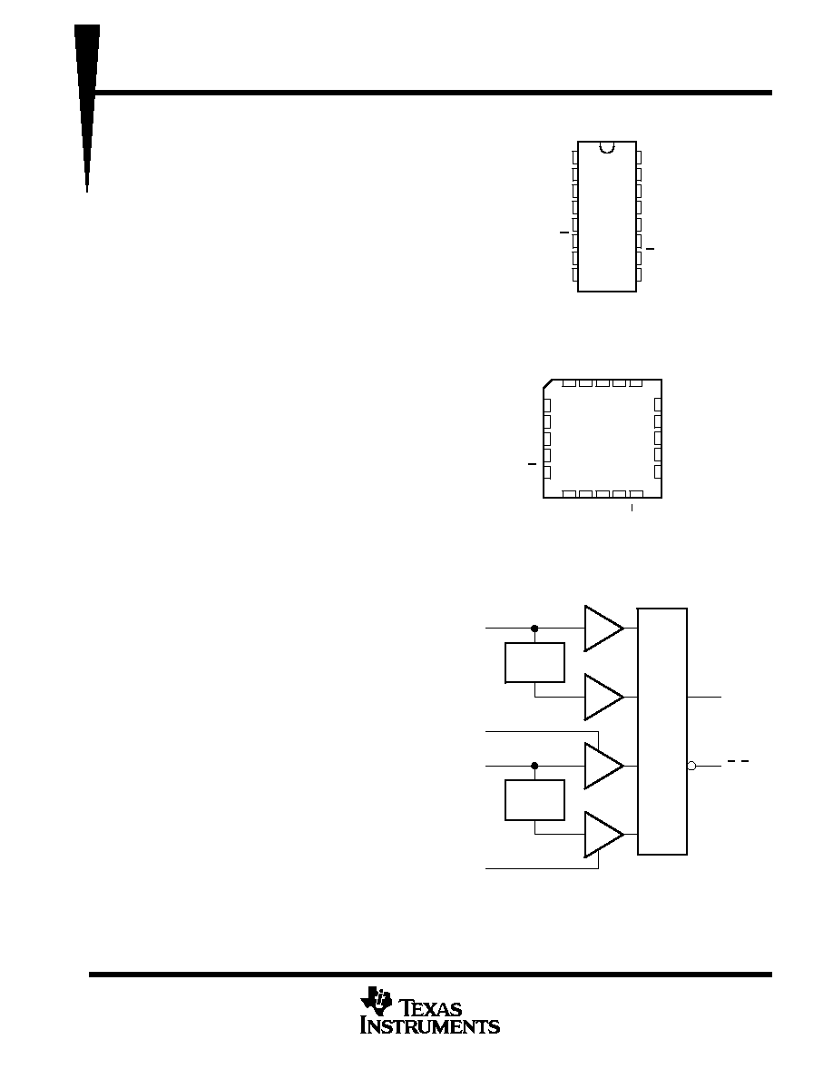
1
2
3
4
5
6
7
8
16
15
14
13
12
11
10
9
C
A2
V
CC ≠
C
A2
A1
Y
Y
A2
V
CC +
NC
C
B2
C
B2
GND
B1
Z
Z
B2
J PACKAGE
(TOP VIEW)
3
2
1 20 19
9 10 11 12 13
4
5
6
7
8
18
17
16
15
14
C
B2
GND
NC
B1
Z
C
A2
A1
NC
Y
Y
FK PACKAGE
(TOP VIEW)
V
C
NC
B2
Z
NC
C
A2
V
NC
NC -- No internal connection
A2
B2
CC +
CC ≠
≠15 dB
≠15 dB
Log
Log
Log
Log
Y (Z)
Y (Z)
A1
(B1)
CA2
(CB2)
CA2
(CB2
)
Y
log A1 + log A2; Z
log B1 + log B2
where: A1, A2, B1, and B2 are in dBV, 0 dBV = 1 V.
CA2, CA2
, CB2, and CB2
are detector compensation inputs.
A2
(B2)
functional block diagram (one half)
TL441AM
LOGARITHMIC AMPLIFIER
SLFS038 ≠ JUNE 1976 ≠ REVISED FEBRUARY 1989
2
POST OFFICE BOX 655303
∑
DALLAS, TEXAS 75265
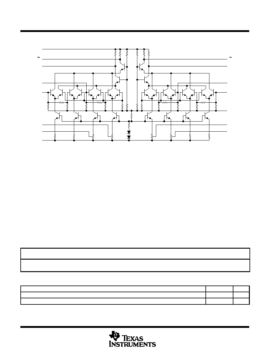
schematic
VCC +
Y
Y
A2
A1
CA2
CA2
VCC ≠
8
6
5
7
4
3
1
2
10
11
9
12
13
14
15
Z
Z
B2
B1
GND
CB2
CB2
Pin numbers shown are for the J package.
absolute maximum ratings over operating free-air temperature range (unless otherwise noted)
Supply voltages (see Note 1): V
CC+
8
V
. . . . . . . . . . . . . . . . . . . . . . . . . . . . . . . . . . . . . . . . . . . . . . . . . . . . . . . . . . .
V
CC ≠
≠ 8
V
. . . . . . . . . . . . . . . . . . . . . . . . . . . . . . . . . . . . . . . . . . . . . . . . . . . . . . . . .
Input voltage (see Note 1)
6 V
. . . . . . . . . . . . . . . . . . . . . . . . . . . . . . . . . . . . . . . . . . . . . . . . . . . . . . . . . . . . . . . . . . . .
Output sink current (any one output)
30 mA
. . . . . . . . . . . . . . . . . . . . . . . . . . . . . . . . . . . . . . . . . . . . . . . . . . . . . . . .
Continuous total dissipation
See Dissipation Rating Table
. . . . . . . . . . . . . . . . . . . . . . . . . . . . . . . . . . . . . . . . . . .
Operating free-air temperature range
≠ 55
∞
C to 125
∞
C
. . . . . . . . . . . . . . . . . . . . . . . . . . . . . . . . . . . . . . . . . . . . . . .
Storage temperature range
≠ 65
∞
C to 150
∞
C
. . . . . . . . . . . . . . . . . . . . . . . . . . . . . . . . . . . . . . . . . . . . . . . . . . . . . . . .
Case temperature for 60 seconds: FK package
260
∞
C
. . . . . . . . . . . . . . . . . . . . . . . . . . . . . . . . . . . . . . . . . . . . . .
Lead temperature 1,6 mm (1/16 inch) from case for 60 seconds: J package
300
∞
C
. . . . . . . . . . . . . . . . . . . . .
Stresses beyond those listed under absolute maximum ratings may cause permanent damage to the device. This is a stress rating only, and
functional operation of the device at these or any other conditions beyond those indicated in the recommended operating conditions section of this
specification is not implied. Exposure to absolute-maximum-rated conditions for extended periods may affect device reliability.
NOTE 1: All voltages, except differential output voltages, are with respect to network ground terminal.
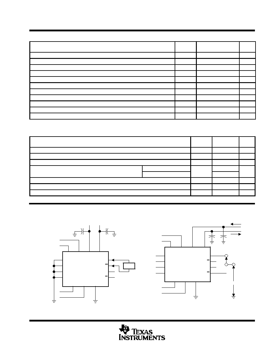
DISSIPATION RATING TABLE
PACKAGE
TA
25
∞
C
POWER RATING
DERATING
FACTOR
DERATE
ABOVE TA
TA = 70
∞
C
POWER RATING
TA = 125
∞
C
POWER RATING
FK
500 mW
11.0 mW/
∞
C
104
∞
C
500 mW
275 mW
J
500 mW
11.0 mW/
∞
C
104
∞
C
500 mW
275 mW
recommended operating conditions
MIN
MAX
UNIT
Peak-to-peak input voltage for each 30-dB stage
0.01
1
V
Operating free-air temperature, TA
≠ 55
125
∞
C
TL441AM
LOGARITHMIC AMPLIFIER
SLFS038 ≠ JUNE 1976 ≠ REVISED FEBRUARY 1989
3
POST OFFICE BOX 655303
∑
DALLAS, TEXAS 75265
electrical characteristics, V
CC
±
=
±
6 V, T
A
= 25
∞
C
PARAMETER
TEST
FIGURE
MIN
TYP
MAX
UNIT
Differential output offset voltage
1
±
25
±
70
mV
Quiescent output voltage
2
5.45
5.6
5.85
V
DC scale factor (differential output), each 3-dB stage, ≠ 35 dBV to ≠ 5 dBV
3
7
8
11
mV/dB
AC scale factor (differential output)
8
mV/dB
DC error at ≠ 20 dBV (midpoint of ≠ 35 dBV to ≠ 5 dBV range)
3
1
2.6
dB
Input impedance
500
Output impedance
200
Rise time, 10% to 90% points, CL = 24 pF
4
20
35
ns
Supply current from VCC+
2
14.5
18.5
23
mA
Supply current from VCC ≠
2
≠ 6
≠ 8.5
≠ 10.5
mA
Power dissipation
2
123
162
201
mW
electrical characteristics over operating free-air temperature range, V
CC
±
=
±
6 V (unless otherwise
noted)
PARAMETER
TEST
FIGURE
MIN
MAX
UNIT
Differential output offset voltage
1
±
100
mV
Quiescent output voltage
2
5.3
5.85
V
DC scale factor (differential output) each 30-dB stage, ≠ 35 dBV to ≠ 5 dBV
3
7
11
mV/dB
DC error at
20 dBV (midpoint of
35 dBV to
5 dBV range)
TA = ≠ 55
∞
C
3
4
dB
DC error at ≠ 20 dBV (midpoint of ≠ 35 dBV to ≠ 5 dBV range)
TA = 125
∞
C
3
3
dB
Supply current from VCC+
2
10
31
mA
Supply current from VCC ≠
2
≠ 4.5
≠ 15
mA
Power dissipation
2
87
276
mW
PARAMETER MEASUREMENT INFORMATION
Figure 1
VCC+
VCC≠
CA2 CA2
VCC + VCC ≠
Y
Y
Z
Z
DVM
CB2 CB2
GND
A1
A2
B1
B2
Figure 2
CA2 CA2
VCC+ VCC≠
Y
Y
Z
Z
CB2 CB2
GND
A1
A2
B1
B2
VCC+
VCC≠
ICC +
ICC ≠
VO
PD = VCC+
∑
ICC+ + VCC≠
∑
ICC≠
TL441AM
LOGARITHMIC AMPLIFIER
SLFS038 ≠ JUNE 1976 ≠ REVISED FEBRUARY 1989
4
POST OFFICE BOX 655303
∑
DALLAS, TEXAS 75265
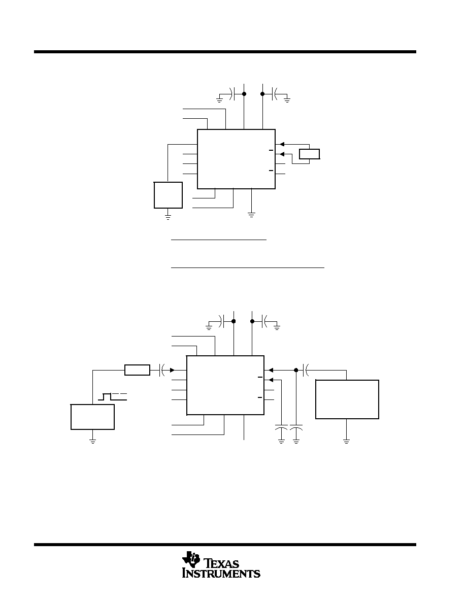
PARAMETER MEASUREMENT INFORMATION
CA2 CA2
VCC+ VCC≠
Y
Y
Z
Z
CB2
GND
A1
A2
B1
B2
DVM
18 mV
100 mV
560 mV
DC
Power
Supply
VCC+ VCC≠
Scale Factor
+
V
out(560 mV)
≠V
out(18mV)
mV
30 dB
Error
+
VV
out(100 mV)
≠0.5 V
out(560 mV)
≠0.5 V
out(18 mV)
Scale Factor
CB2
Figure 3
CA2 CA2
VCC+ VCC≠
Y
Y
Z
Z
CB2 CB2
GND
A1
A2
B1
B2
VCC+
VCC≠
1000 pF
CI
CL
CL
100 mV
0 mV
Atten
Pulse
Generator
50
Tektronix
Sampling Scope
With Digital
Readout or
Equivalent
NOTES: A. The input pulse has the following characteristics: tw = 200 ns, tr
2 ns, tf
2 ns, PRR
10 MHz.
B. Capacitor CI consists of three capacitors in parallel: 1
µ
F, 0.1
µ
F, and 0.01
µ
F.
C. CL includes probe and jig capacitance.
Figure 4
TL441AM
LOGARITHMIC AMPLIFIER
SLFS038 ≠ JUNE 1976 ≠ REVISED FEBRUARY 1989
5
POST OFFICE BOX 655303
∑
DALLAS, TEXAS 75265
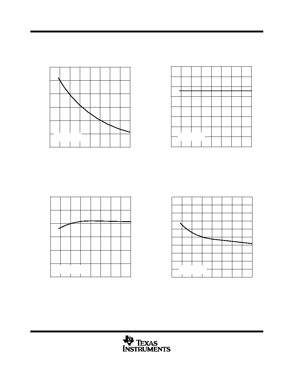
TYPICAL CHARACTERISTICS
Figure 5
DIFFERENTIAL OUTPUT OFFSET VOLTAGE
vs
FREE-AIR TEMPERATURE
TA ≠ Free-Air Temperature ≠
∞
C
60
50
40
30
20
10
0
≠ 75 ≠ 50 ≠ 25
0
25
50
75
100
125
Differential Output Offset V
oltage ≠ mV
VCC
±
=
±
6 V
See Figure 1
Figure 6
QUIESCENT OUTPUT VOLTAGE
vs
FREE-AIR TEMPERATURE
TA ≠ Free-Air Temperature ≠
∞
C
≠ 75 ≠ 50 ≠ 25
0
25
50
75
100
125
8
7
6
5
4
3
2
1
0
Quiescent Output V
oltage ≠ V
VCC
±
=
±
6 V
See Figure 2
Figure 7
TA ≠ Free-Air Temperature ≠
∞
C
≠ 75 ≠ 50 ≠ 25
0
25
50
75
100
125
12
10
8
6
4
2
0
DC SCALE FACTOR
vs
FREE-AIR TEMPERATURE
DC Scale Factor (Differential Output) ≠ mV/dBV
VCC
±
=
±
6 V
See Figure 3
Figure 8
TA ≠ Free-Air Temperature ≠
∞
C
≠ 75 ≠ 50 ≠ 25
0
25
50
75
100
125
2.0
1.8
1.6
1.4
1.2
1.0
0.8
0.6
0.4
0.2
0
DC ERROR
vs
FREE-AIR TEMPERATURE
DC Error at Midpoint of 30-dBV Range ≠ dBV
VCC
±
=
±
6 V
See Figure 3