 | ÐлекÑÑоннÑй компоненÑ: TLC32046I | СкаÑаÑÑ:  PDF PDF  ZIP ZIP |
Äîêóìåíòàöèÿ è îïèñàíèÿ www.docs.chipfind.ru

TLC32046C, TLC32046I, TLC32046M
Data Manual
Wide-Band Analog Interface Circuit
SLAS028
May 1995

IMPORTANT NOTICE
Texas Instruments (TI) reserves the right to make changes to its products or to discontinue any
semiconductor product or service without notice, and advises its customers to obtain the latest
version of relevant information to verify, before placing orders, that the information being relied
on is current.
TI warrants performance of its semiconductor products and related software to the specifications
applicable at the time of sale in accordance with TI's standard warranty. Testing and other quality
control techniques are utilized to the extent TI deems necessary to support this warranty.
Specific testing of all parameters of each device is not necessarily performed, except those
mandated by government requirements.
Certain applications using semiconductor products may involve potential risks of death,
personal injury, or severe property or environmental damage ("Critical Applications").
TI SEMICONDUCTOR PRODUCTS ARE NOT DESIGNED, INTENDED, AUTHORIZED, OR
WARRANTED TO BE SUITABLE FOR USE IN LIFE-SUPPORT APPLICATIONS, DEVICES
OR SYSTEMS OR OTHER CRITICAL APPLICATIONS.
Inclusion of TI products in such applications is understood to be fully at the risk of the customer.
Use of TI products in such applications requires the written approval of an appropriate TI officer.
Questions concerning potential risk applications should be directed to TI through a local SC
sales office.
In order to minimize risks associated with the customer's applications, adequate design and
operating safeguards should be provided by the customer to minimize inherent or procedural
hazards.
TI assumes no liability for applications assistance, customer product design, software
performance, or infringement of patents or services described herein. Nor does TI warrant or
represent that any license, either express or implied, is granted under any patent right, copyright,
mask work right, or other intellectual property right of TI covering or relating to any combination,
machine, or process in which such semiconductor products or services might be or are used.
Copyright
©
1995, Texas Instruments Incorporated

iii
Contents
Section
Title
Page
1
Introduction
11
. . . . . . . . . . . . . . . . . . . . . . . . . . . . . . . . . . . . . . . . . . . . . . . . . . . . . . . . . . . . . .
1.1
Features
12
. . . . . . . . . . . . . . . . . . . . . . . . . . . . . . . . . . . . . . . . . . . . . . . . . . . . . . . . . . . . .
1.2
Functional Block Diagrams
13
. . . . . . . . . . . . . . . . . . . . . . . . . . . . . . . . . . . . . . . . . . . . .
1.3
Terminal Assignments
16
. . . . . . . . . . . . . . . . . . . . . . . . . . . . . . . . . . . . . . . . . . . . . . . . .
1.4
Ordering Information
16
. . . . . . . . . . . . . . . . . . . . . . . . . . . . . . . . . . . . . . . . . . . . . . . . . .
1.5
Terminal Functions
17
. . . . . . . . . . . . . . . . . . . . . . . . . . . . . . . . . . . . . . . . . . . . . . . . . . . .
2
Detailed Description
21
. . . . . . . . . . . . . . . . . . . . . . . . . . . . . . . . . . . . . . . . . . . . . . . . . . . . . .
2.1
Internal Timing Configuration
22
. . . . . . . . . . . . . . . . . . . . . . . . . . . . . . . . . . . . . . . . . . .
2.2
Analog Input
24
. . . . . . . . . . . . . . . . . . . . . . . . . . . . . . . . . . . . . . . . . . . . . . . . . . . . . . . . .
2.3
A/D Band-Pass Filter, Clocking, and Conversion Timing
24
. . . . . . . . . . . . . . . . . . . .
2.4
A/D Converter
24
. . . . . . . . . . . . . . . . . . . . . . . . . . . . . . . . . . . . . . . . . . . . . . . . . . . . . . . .
2.5
Analog Output
24
. . . . . . . . . . . . . . . . . . . . . . . . . . . . . . . . . . . . . . . . . . . . . . . . . . . . . . . .
2.6
D/A Low-Pass Filter, Clocking, and Conversion Timing
24
. . . . . . . . . . . . . . . . . . . . .
2.7
D/A Converter
24
. . . . . . . . . . . . . . . . . . . . . . . . . . . . . . . . . . . . . . . . . . . . . . . . . . . . . . . .
2.8
Serial Port
25
. . . . . . . . . . . . . . . . . . . . . . . . . . . . . . . . . . . . . . . . . . . . . . . . . . . . . . . . . . .
2.9
Synchronous Operation
25
. . . . . . . . . . . . . . . . . . . . . . . . . . . . . . . . . . . . . . . . . . . . . . . .
2.9.1
One 16-Bit Word
25
. . . . . . . . . . . . . . . . . . . . . . . . . . . . . . . . . . . . . . . . . . . . . . .
2.9.2
Two 8-Bit Bytes
25
. . . . . . . . . . . . . . . . . . . . . . . . . . . . . . . . . . . . . . . . . . . . . . .
2.9.3
Synchronous Operating Frequencies
26
. . . . . . . . . . . . . . . . . . . . . . . . . . . . .
2.10 Asynchronous Operation
26
. . . . . . . . . . . . . . . . . . . . . . . . . . . . . . . . . . . . . . . . . . . . . . .
2.10.1 One 16-Bit Word
26
. . . . . . . . . . . . . . . . . . . . . . . . . . . . . . . . . . . . . . . . . . . . . . .
2.10.2 Two 8-Bit Bytes
26
. . . . . . . . . . . . . . . . . . . . . . . . . . . . . . . . . . . . . . . . . . . . . . . .
2.10.3 Asynchronous Operating Frequencies
26
. . . . . . . . . . . . . . . . . . . . . . . . . . . .
2.11 Operation of TLC32046C and TLC32046I With Internal Voltage Reference
27
. . .
2.12 Operation of TLC32046C AND TLC32046I With External Voltage Reference
27
.
2.13 Reset
27
. . . . . . . . . . . . . . . . . . . . . . . . . . . . . . . . . . . . . . . . . . . . . . . . . . . . . . . . . . . . . . .
2.14 Loopback
27
. . . . . . . . . . . . . . . . . . . . . . . . . . . . . . . . . . . . . . . . . . . . . . . . . . . . . . . . . . . .
2.15 Communications Word Sequence
28
. . . . . . . . . . . . . . . . . . . . . . . . . . . . . . . . . . . . . . .
2.15.1 Primary DR Word Bit Pattern
28
. . . . . . . . . . . . . . . . . . . . . . . . . . . . . . . . . . . .
2.15.2 Primary DX Word Bit Pattern
29
. . . . . . . . . . . . . . . . . . . . . . . . . . . . . . . . . . . .
2.15.3 Secondary DX Word Bit Pattern
210
. . . . . . . . . . . . . . . . . . . . . . . . . . . . . . . . .
2.16 Reset Function
210
. . . . . . . . . . . . . . . . . . . . . . . . . . . . . . . . . . . . . . . . . . . . . . . . . . . . . . .
2.17 Power-Up Sequence
211
. . . . . . . . . . . . . . . . . . . . . . . . . . . . . . . . . . . . . . . . . . . . . . . . . .
2.18 AIC Register Constraints
211
. . . . . . . . . . . . . . . . . . . . . . . . . . . . . . . . . . . . . . . . . . . . . . .
2.19 AIC Responses to Improper Conditions
211
. . . . . . . . . . . . . . . . . . . . . . . . . . . . . . . . . .
2.20 Operation With Conversion Times Too Close Together
212
. . . . . . . . . . . . . . . . . . . . .
2.21 More Than One Receive Frame Sync Occurring Between Two Transmit
Frame Syncs Asynchronous Operation
212
. . . . . . . . . . . . . . . . . . . . . . . . . . . . . . . . .
2.22 More Than One Transmit Frame Sync Occurring Between Two Receive
Frame Syncs Asynchronous Operation
213
. . . . . . . . . . . . . . . . . . . . . . . . . . . . . . . . .

iv
Section
Title
Page
2.23 More than One Set of Primary and Secondary DX Serial Communications
Occurring Between Two Receive Frame Syncs Asynchronous Operation
213
. . .
2.24 System Frequency Response Correction
214
. . . . . . . . . . . . . . . . . . . . . . . . . . . . . . . . .
2.25 (Sin x)/x Correction
214
. . . . . . . . . . . . . . . . . . . . . . . . . . . . . . . . . . . . . . . . . . . . . . . . . . .
2.26 (Sin x)/x Roll-Off for a Zero-Order Hold Function
214
. . . . . . . . . . . . . . . . . . . . . . . . . .
2.27 Correction Filter
215
. . . . . . . . . . . . . . . . . . . . . . . . . . . . . . . . . . . . . . . . . . . . . . . . . . . . . .
2.28 Correction Results
215
. . . . . . . . . . . . . . . . . . . . . . . . . . . . . . . . . . . . . . . . . . . . . . . . . . . .
2.29 TMS320 Software Requirements
216
. . . . . . . . . . . . . . . . . . . . . . . . . . . . . . . . . . . . . . . .
3
Specifications
31
. . . . . . . . . . . . . . . . . . . . . . . . . . . . . . . . . . . . . . . . . . . . . . . . . . . . . . . . . . . .
3.1
Absolute Maximum Ratings Over Operating Free-Air Temperature Range
31
. . . .
3.2
Recommended Operating Conditions
31
. . . . . . . . . . . . . . . . . . . . . . . . . . . . . . . . . . . .
3.3
Electrical Characteristics Over Recommended Operating Free-Air
Temperature Range, V
CC+
= 5 V, V
CC
= 5 V, V
DD
= 5 V
32
. . . . . . . . . . . . . . . . .
3.3.1
Total Device, MSTR CLK Frequency = 5.184 MHz
32
. . . . . . . . . . . . . . . . .
3.3.2
Power Supply Rejection and Crosstalk Attenuation
32
. . . . . . . . . . . . . . . . .
3.3.3
Serial Port
32
. . . . . . . . . . . . . . . . . . . . . . . . . . . . . . . . . . . . . . . . . . . . . . . . . . . .
3.3.4
Receive Amplifier Input
33
. . . . . . . . . . . . . . . . . . . . . . . . . . . . . . . . . . . . . . . . .
3.3.5
Transmit Filter Output
33
. . . . . . . . . . . . . . . . . . . . . . . . . . . . . . . . . . . . . . . . . .
3.3.6
Receive and Transmit Channel System Distortion, SCF Clock
Frequency = 288 kHz
33
. . . . . . . . . . . . . . . . . . . . . . . . . . . . . . . . . . . . . . . . . . .
3.3.7
Receive Channel Signal-to-Distortion Ratio
34
. . . . . . . . . . . . . . . . . . . . . . .
3.3.8
Transmit Channel Signal-to-Distortion Ratio
34
. . . . . . . . . . . . . . . . . . . . . . .
3.3.9
Receive and Transmit Gain and Dynamic Range
34
. . . . . . . . . . . . . . . . . . .
3.3.10 Receive Channel Band-Pass Filter Transfer Function,
SCF f
clock
= 288 kHz, Input (IN+ IN ) Is A + 3-V Sine Wave
35
. . . . . . .
3.3.11 Receive and Transmit Channel Low-Pass Filter Transfer Function,
SCF f
clock
= 288 kHz
35
. . . . . . . . . . . . . . . . . . . . . . . . . . . . . . . . . . . . . . . . . . .
3.4
Operating Characteristics Over Recommended Operating Free-Air
Temperature Range, V
CC+
= 5 V, V
CC
= 5 V, V
DD
= 5 V
36
. . . . . . . . . . . . . . . . .
3.4.1 Receive and Transmit Noise
36
. . . . . . . . . . . . . . . . . . . . . . . . . . . . . . . . . . . . . .
3.5
Timing Requirements
36
. . . . . . . . . . . . . . . . . . . . . . . . . . . . . . . . . . . . . . . . . . . . . . . . . .
3.5.1
Serial Port Recommended Input Signals
36
. . . . . . . . . . . . . . . . . . . . . . . . . .
3.5.2
Serial Port AIC Output Signals, C
L
= 30 pF for SHIFT CLK Output,
C
L
= 15 pF For All Other Outputs
37
. . . . . . . . . . . . . . . . . . . . . . . . . . . . . . . .
4
Parameter Measurement Information
41
. . . . . . . . . . . . . . . . . . . . . . . . . . . . . . . . . . . . . . .
5
Typical Characteristics
51
. . . . . . . . . . . . . . . . . . . . . . . . . . . . . . . . . . . . . . . . . . . . . . . . . . . .
6
Application Information
61
. . . . . . . . . . . . . . . . . . . . . . . . . . . . . . . . . . . . . . . . . . . . . . . . . . .

v
List of Illustrations
Figure
Title
Page
11
Dual-Word (Telephone Interface) Mode
15
. . . . . . . . . . . . . . . . . . . . . . . . . . . . . . . . . . .
12
Word Mode
15
. . . . . . . . . . . . . . . . . . . . . . . . . . . . . . . . . . . . . . . . . . . . . . . . . . . . . . . . . . .
13
Byte Mode
15
. . . . . . . . . . . . . . . . . . . . . . . . . . . . . . . . . . . . . . . . . . . . . . . . . . . . . . . . . . . .
21
Asynchronous Internal Timing Configuration
23
. . . . . . . . . . . . . . . . . . . . . . . . . . . . . . .
22
Primary and Secondary Communications Word Sequence
28
. . . . . . . . . . . . . . . . . . .
23
DR Word Bit Pattern
28
. . . . . . . . . . . . . . . . . . . . . . . . . . . . . . . . . . . . . . . . . . . . . . . . . . . .
24
Primary DX Word BIt Pattern
29
. . . . . . . . . . . . . . . . . . . . . . . . . . . . . . . . . . . . . . . . . . . .
25
Secondary DX Word BIt Pattern
210
. . . . . . . . . . . . . . . . . . . . . . . . . . . . . . . . . . . . . . . . . .
26
Reset on Power-Up Circuit
211
. . . . . . . . . . . . . . . . . . . . . . . . . . . . . . . . . . . . . . . . . . . . . .
27
Conversion Times Too Close Together
212
. . . . . . . . . . . . . . . . . . . . . . . . . . . . . . . . . . . .
28
More Than One Receive Frame Sync Between Two Transmit Frame Syncs
213
. . .
29
More Than One Transmit Frame Sync Between Two Receive Frame Syncs
213
. . .
210 More Than One Set of Primary and Secondary DX Serial Communications
Between Two Receive Frame Syncs
214
. . . . . . . . . . . . . . . . . . . . . . . . . . . . . . . . . . . . . .
211 First-Order Correction Filter
215
. . . . . . . . . . . . . . . . . . . . . . . . . . . . . . . . . . . . . . . . . . . . .
41
IN + and IN Gain Control Circuitry
41
. . . . . . . . . . . . . . . . . . . . . . . . . . . . . . . . . . . . . . .
42
Dual-Word (Telephone Interface) Mode Timing
42
. . . . . . . . . . . . . . . . . . . . . . . . . . . . .
43
Word Timing
42
. . . . . . . . . . . . . . . . . . . . . . . . . . . . . . . . . . . . . . . . . . . . . . . . . . . . . . . . . . .
4 4
Byte Mode Timing
43
. . . . . . . . . . . . . . . . . . . . . . . . . . . . . . . . . . . . . . . . . . . . . . . . . . . . . .
4 5
Shift-Clock Timing
44
. . . . . . . . . . . . . . . . . . . . . . . . . . . . . . . . . . . . . . . . . . . . . . . . . . . . . .
4 6
TMS32010/TMS320C15 TLC32046 Interface Timing
44
. . . . . . . . . . . . . . . . . . . . . .
4 7
TMS32010/TMS320C15 TLC32046 Interface Circuit
45
. . . . . . . . . . . . . . . . . . . . . . .

vi
List of Tables
Table
Title
Page
21
Mode-Selection Function Table
21
. . . . . . . . . . . . . . . . . . . . . . . . . . . . . . . . . . . . . . . . . .
22
Primary DX Serial Communication Protocol
21
. . . . . . . . . . . . . . . . . . . . . . . . . . . . . . . .
23
Secondary DX Serial Communication Protocol
21
. . . . . . . . . . . . . . . . . . . . . . . . . . . . .
24
AIC Responses to Improper Conditions
21
. . . . . . . . . . . . . . . . . . . . . . . . . . . . . . . . . . .
25
(sin x)/x Roll-Off Error
21
. . . . . . . . . . . . . . . . . . . . . . . . . . . . . . . . . . . . . . . . . . . . . . . . . .
26
(sin x)/x Correction Table for f
s
= 8000 Hz and f
s
= 9600 Hz
21
. . . . . . . . . . . . . . . . .
41
Gain Control Table
41
. . . . . . . . . . . . . . . . . . . . . . . . . . . . . . . . . . . . . . . . . . . . . . . . . . . . .

11
1 Introduction
The TLC32046C, TLC32046I, and TLC32046M wide-band analog interface circuits (AIC) are a complete
analog-to-digital and digital-to-analog interface system for advanced digital signal processors (DSPs)
similar to the TMS32020, TMS320C25, and TMS320C30. The TLC32046C and TLC32046I offer a powerful
combination of options under DSP control: three operating modes (dual-word [telephone interface], word,
and byte) combined with two word formats (8 bits and 16 bits) and synchronous or asynchronous operation.
It provides a high level of flexibility in that conversion and sampling rates, filter bandwidths, input circuitry,
receive and transmit gains, and multiplexed analog inputs are under processor control.
This AIC features a
·
band-pass switched-capacitor antialiasing input filter
·
14-bit-resolution A/D converter
·
14-bit-resolution D/A converter
·
low-pass switched-capacitor output-reconstruction filter.
The antialiasing input filter comprises eighth-order and fourth-order CC-type (Chebyshev/elliptic
transitional) low-pass and high-pass filters, respectively. The input filter is implemented in switched-
capacitor technology and is preceded by a continuous time filter to eliminate any possibility of aliasing
caused by sampled data filtering. When low-pass filtering is desired, the high-pass filter can be switched
out of the signal path. A selectable auxiliary differential analog input is provided for applications where more
than one analog input is required.
The output-reconstruction filter is an eighth-order CC-type (Chebyshev/elliptic transitional low-pass filter)
followed by a second-order (sin x)/x correction filter and is implemented in switched-capacitor technology.
This filter is followed by a continuous-time filter to eliminate images of the sample data signal. The on-board
(sin x)/x correction filter can be switched out of the signal path using digital signal processor control.
The A/D and D/A architectures ensure no missing codes and monotonic operation. An internal voltage
reference is provided to ease the design task and to provide complete control over the performance of the
IC. The internal voltage reference is brought out to REF. Separate analog and digital voltage supplies and
ground are provided to minimize noise and ensure a wide dynamic range. The analog circuit path contains
only differential circuitry to keep noise to a minimum. The exception is the DAC sample-and-hold, which
utilizes pseudo-differential circuitry.
The TLC32046C is characterized for operation from 0
°
C to 70
°
C, the TLC32046I is characterized for
operation from 40
°
C to 85
°
C, and the TLC32046M is characterized for operation from 55
°
C to 125
°
C.

12
1.1
Features
·
14-Bit Dynamic Range ADC and DAC
·
16-Bit Dynamic Range Input With Programmable Gain
·
Synchronous or Asynchronous ADC and DAC Sampling Rates Up to 25,000 Samples Per
Second
·
Programmable Incremental ADC and DAC Conversion Timing Adjustments
·
Typical Applications
Speech Encryption for Digital Transmission
Speech Recognition and Storage Systems
Speech Synthesis
Modems at 8-kHz, 9.6-kHz, and 16-kHz Sampling Rates
Industrial Process Control
Biomedical Instrumentation
Acoustical Signal Processing
Spectral Analysis
Instrumentation Recorders
Data Acquisition
·
Switched-Capacitor Antialiasing Input Filter and Output-Reconstruction Filter
·
Three Fundamental Modes of Operation: Dual-Word (Telephone Interface), Word, and Byte
·
600-mil Wide N Package
·
Digital Output in Twos Complement Format
·
CMOS Technology
FUNCTION TABLE
DATA
COMMUNICATIONS
FORMAT
SYNCHRONOUS
(CONTROL
REGISTER
BIT D5 = 1)
ASYNCHRONOUS
(CONTROL
REGISTER
BIT D5 = 0)
FORCING CONDITION
DIRECT
INTERFACE
16-bit format
Dual-word
(telephone
interface) mode
Dual-word
(telephone interface)
mode
Terminal 13 = 0 to 5 V
Terminal 1 = 0 to 5 V
TMS32020,
TMS320C25,
TMS320C30
16-bit format
Word mode
Word mode
Terminal 13 = VCC ( 5 V nom)
Terminal 1 = VCC+ (5 V nom)
TMS32020,
TMS320C25,
TMS320C30,
indirect
interface to
TMS320C10.
(see Figure 7).
8-bit format
(2 bytes required)
Byte mode
Byte mode
Terminal 13 = VCC ( 5 V nom)
Terminal 1 = VCC ( 5 V nom)
TMS320C17
13
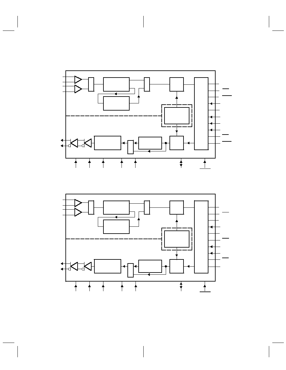
1.2
Functional Block Diagrams
WORD OR BYTE MODE
Transmit Section
OUT
OUT +
AUX IN
AUX IN +
IN
IN +
D/A
EODX
FSX
DX
CONTROL
WORD-
BYTE
SHIFT CLK
MSTR CLK
EODR
DR
FSR
RESET
REF
(DIGITAL)
VDD
GND
DGTL
GND
ANLG
VCC
VCC +
X
U
M
Correction
(sin x)/x
Port
Serial
Reference
Voltage
Internal
A/D
Receive Section
M
U
X
X
U
M
DUAL-WORD (TELEPHONE INTERFACE) MODE
OUT
OUT +
AUX IN
AUX IN +
IN
IN +
D/A
FSX
DX
SHIFT CLK
MSTR CLK
DR
FSR
RESET
REF
(DIGITAL)
VDD
GND
DGTL
GND
ANLG
VCC
VCC +
X
U
M
Correction
(sin x)/x
Port
Serial
Reference
Voltage
Internal
A/D
M
U
X
X
U
M
D11 OUT
FSD
DATA DR
D10 OUT
Receive Section
Transmit Section
Low-Pass
Filter
High-Pass
Filter
Low-Pass
Filter
Low-Pass
Filter
High-Pass
Filter
Low-Pass
Filter
26
25
24
23
22
21
5
4
3
6
10
1
13
12
14
11
20
19
9
7
8
2
20
19
17,18
9
7
8
2
26
25
24
23
22
21
5
4
3
6
10
1
13
12
14
11
17,18
14
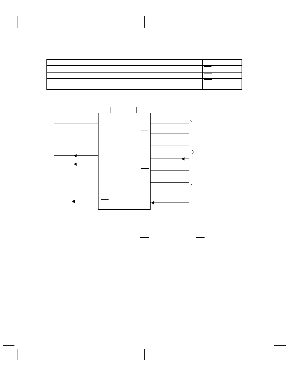
FRAME SYNCHRONIZATION FUNCTIONS
Function
Frame Sync Output
Receiving serial data on DX from processor to internal DAC
FSX low
Transmitting serial data on DR from internal ADC to processor, primary communications
FSR low
Transmitting serial data on DR from Data-DR to processor, secondary communications in
dual-word (telephone interface) mode only
FSD low
TLC32046
Logic Levels
TTL or CMOS
TMS32020,
TMS320C25,
TMS320C30, or
Equivalent 16-Bit DSP
5 V
5 V
FSD
D11OUT
Serial Data Out
DR
Serial Data In
DX
DATA-DR
or CMOS Logic Levels
16-Bit Format TTL
Secondary Communication (see Table above)
Serial Data Input
Analog Out
Analog In
OUT
OUT +
IN
IN +
FSR
D10OUT
FSX
VCC
VCC +
20
19
26
25
22
21
1
5
4
3
12
14
11
13
Figure 11. Dual-Word (Telephone Interface) Mode
When the DATA-DR/CONTROL input is tied to a logic signal source varying between 0 and 5 V, the
TLC32046 is in the dual-word (telephone interface) mode. This logic signal is routed to the DR line for input
to the DSP only when data frame synchronization (FSD) outputs a low level. The FSD pulse duration is 16
shift clock pulses. Also, in this mode, the control register data bits D10 and D11 appear on D10OUT and
D11OUT, respectively, as outputs.
15
TLC32046
Logic Levels
TTL or CMOS
TMS320C30,
or Equivalent
16-Bit DSP
TMS320C25,
TMS32020,
5 V
5 V
EODR
Serial Data Out
DR
Serial Data In
DX
CONTROL
Analog Out
Analog In
OUT
OUT +
IN
IN +
FSR
FSX
VCC
VCC +
EODX
( 5 V nom)
(5 V nom)
WORD-BYTE
VCC
VCC+
26
25
22
21
1
20
19
5
4
3
12
14
11
13
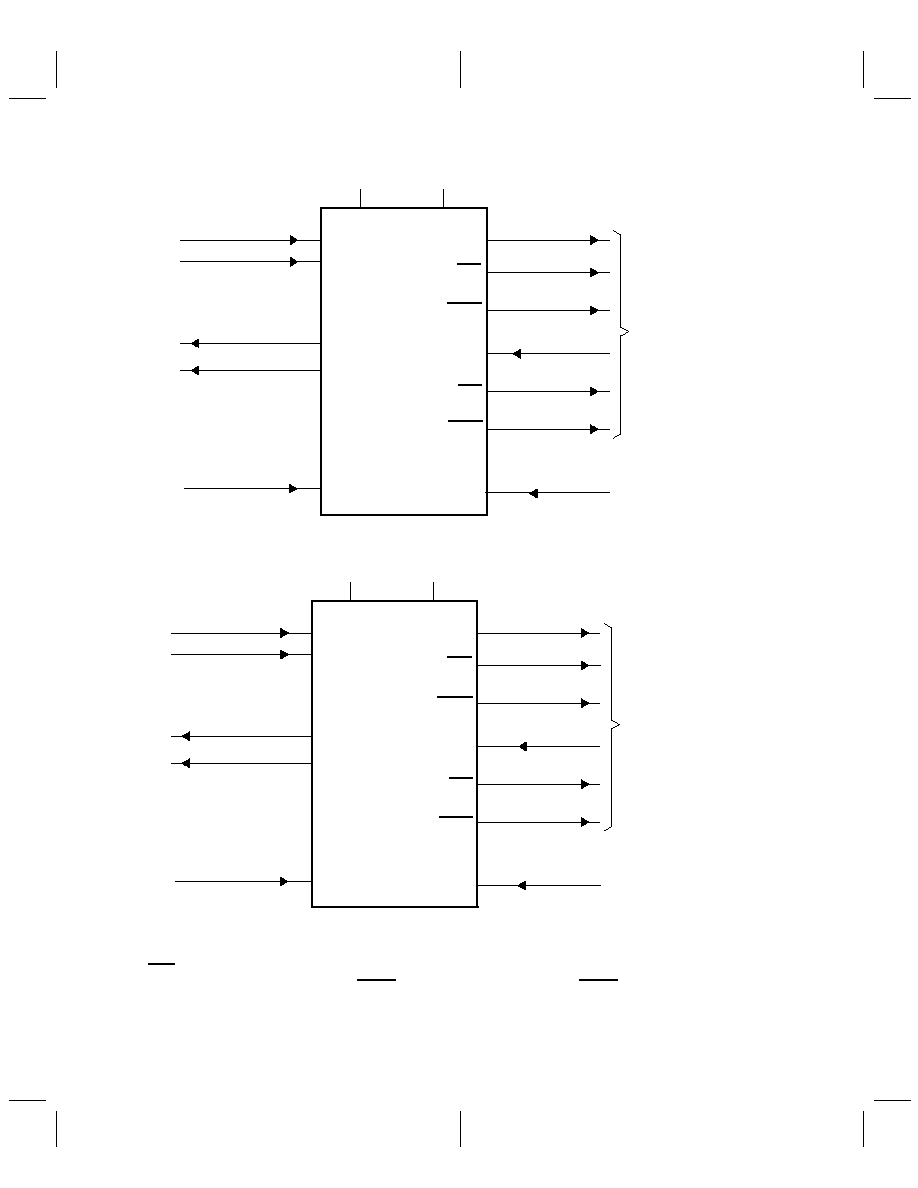
Figure 12. Word Mode
TLC32046
5 V
5 V
EODR
Serial Data Out
DR
Serial Data In
DX
CONTROL
Analog Out
Analog In
OUT
OUT+
IN
IN +
FSR
FSX
VCC
VCC +
EODX
( 5 V nom)
( 5 V nom)
WORD-BYTE
TMS320C17 or
Equivalent
8-Bit Serial Interface
(2 bytes required)
Logic Levels
TTL or CMOS
VCC
VCC
26
25
22
21
1
20
19
5
4
3
12
14
11
13
Figure 13. Byte Mode
The word or byte mode is selected by first connecting the DATA-DR/CONTROL input to V
CC.
FSD/WORD-BYTE becomes an input and can then be used to select either word or byte transmission
formats. The end-of-data transmit (EODX) and the end-of-data receive (EODR) signals respectively, are
used to signal the end of word or byte communication (see the Terminal Functions section).
16
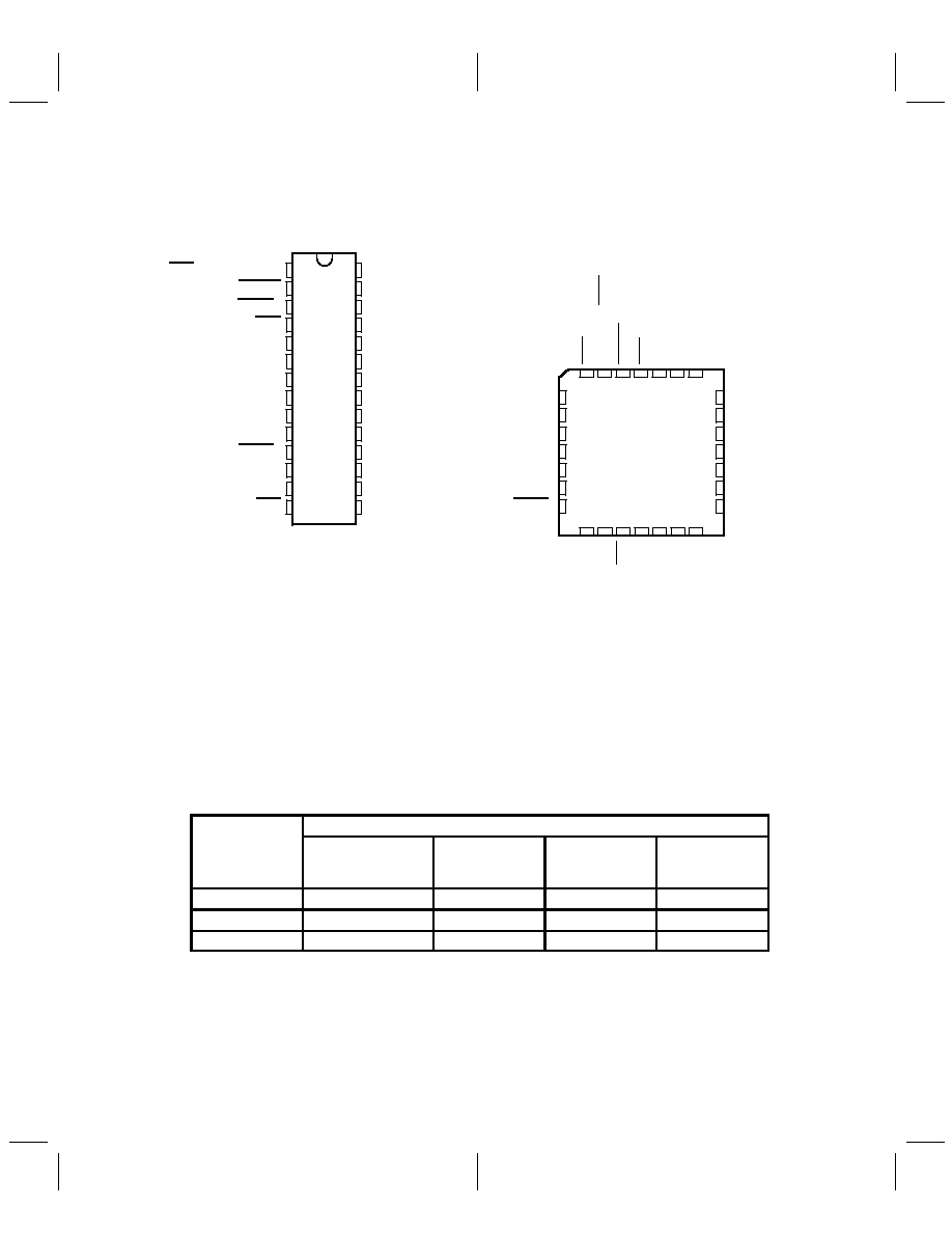
1.3
Terminal Assignments
1
2
3
4
5
6
7
8
9
10
11
12
13
14
28
27
26
25
24
23
22
21
20
19
18
17
16
15
FSD/WORD-BYTE§
RESET
D11OUT/EODR§
FSR
DR
MSTR CLK
VDD
REF
DGTL GND
SHIFT CLK
D10OUT/EODX§
DX
DATA-DR/CONTROL§
FSX
NU
NU
IN+
IN
AUX IN+
AUX IN
OUT+
OUT
VCC+
VCC
ANLG GND
ANLG GND
NU
NU
J OR N PACKAGE
(TOP VIEW)
3 2 1 28 27
12 13
5
6
7
8
9
10
11
25
24
23
22
21
20
19
IN
AUX IN+
AUX IN
OUT+
OUT
VCC+
VCC
DR
MSTR CLK
VDD
REF
DGTL GND
SHIFT CLK
D10OUT/EODX§
4
26
14 15 16 17 18
DX
FSX
NU
NU
ANLG GND
ANLG GND
D1
1OUOT/EODR
NU
NU
IN+
FK OR FN PACKAGE
(TOP VIEW)
NU - Nonusable; no external connection should be made to these terminals.
RESET
FSR
FSD/WORD-BYTE
DA
T
A-DR/CONTROL
§
§
§
Refer to the mechanical data for the JT package.
600-mil wide
§ The portion of the terminal name to the left of the slash is used for the dual-word (telephone interface) mode.
The portion of the terminal name to the right of the slash is used for word-byte mode.
1.4
Ordering Information
AVAILABLE OPTIONS
PACKAGE
TA
PLASTIC CHIP
CARRIER
(FN)
PLASTIC DIP
(N)
CERAMIC DIP
(J)
CHIP CARRIER
(FK)
0
°
C to 70
°
C
TLC32046CFN
TLC32046CN
40
°
C to 85
°
C
TLC32046IFN
TLC32046IN
55
°
C to 125
°
C
TLC32046MJ
TLC32046MFK
17
1.5
Terminal Functions
TERMINAL
I/O
DESCRIPTION
NAME
NO.
I/O
DESCRIPTION
ANLG GND
17,18
Analog ground return for all internal analog circuits. Not internally connected to DGTL
GND.
AUX IN +
24
I
Noninverting auxiliary analog input stage. AUX IN+ can be switched into the band-pass
filter and ADC path via software control. If the appropriate bit in the control register is
a 1, the auxiliary inputs replace the IN + and IN inputs. If the bit is a 0, the IN + and IN
inputs are used (see the DX Serial Data Word Format).
AUX IN
23
I
Inverting auxiliary analog input (see the above AUX IN + description).
DATA-DR
13
I
The dual-word (telephone interface) mode, selected by applying an input logic level
between 0 and 5 V to DATA-DR, allows this terminal to function as a data input. The data
is then framed by the FSD signal and transmitted as an output to the DR line during
secondary communication. The functions FSD, D11OUT, and D10OUT are valid with
this mode selection (see Table 21).
CONTROL
When CONTROL is tied to VCC , the device is in the word or byte mode. The functions
WORD-BYTE, EODR, and EODX are valid in this mode. CONTROL is then used to
select either the word or byte mode (see Function Table).
DR
5
O
DR is used to transmit the ADC output bits from the AIC to the TMS320 serial port. This
transmission of bits from the AIC to the TMS320 serial port is synchronized with
SHIFT CLK.
DX
12
I
DX is used to receive the DAC input bits and timing and control information from the
TMS320. This serial transmission from the TMS320 serial port is synchronized with
SHIFT CLK.
D10OUT
11
O
In the dual-word (telephone interface) mode, bit D10 of the control register is output to
D10OUT. When the device is reset, bit D10 is initialized to 0 (see DX Serial Data Word
Format). The output update is immediate upon changing bit D10.
EODX
End-of-data transmit. During the word-mode timing, a low-going pulse occurs on EODX
immediately after the 16 bits of DAC and control or register information have transmitted
from the TMS320 serial port to the AIC.This signal can be used to interrupt a
microprocessor upon completion of serial communications. Also, this signal can be
used to strobe and enable external serial-to-parallel shift registers, latches, or external
FIFO RAM and to facilitate parallel data bus communications between the DSP and the
serial-to-parallel shift registers. During the byte-mode timing, this signal goes low after
the first byte has been transmitted from the TMS320 serial port to the AIC and is kept
low until the second byte has been transmitted. The TMS320C17 can use this low-going
signal to differentiate first and second bytes.
D11OUT
3
O
In the dual-word (telephone interface) mode, bit D11 of the control register is output to
D11OUT. When the device is reset, bit D11 is initialized to 0 (see DX Serial Data Word
Format). The output update is immediate upon changing bit D11.
EODR
End-of-data receive. During the word-mode timing, a low-going pulse occurs on EODR
immediately after the 16 bits of A/D information have been transmitted from the AIC to
the TMS320 serial port. This signal can be used to interrupt a microprocessor upon
completion of serial communications. Also, this signal can be used to strobe and enable
external serial-to-parallel shift registers, latches, or external FIFO RAM, and to facilitate
parallel data bus communications between the DSP and the serial-to-parallel shift
registers. During the byte-mode timing, this signal goes low after the first byte has been
transmitted from the AIC to the TMS320 serial port and is kept low until the second byte
has been transmitted. The TMS320C17 can use this low-going signal to differentiate
between first and second bytes.
18
1.5
Terminal Functions (continued)
TERMINAL
I/O
DESCRIPTION
NAME
NO.
I/O
DESCRIPTION
DGTL
9
Digital ground for all internal logic circuits. Not internally connected to ANLG GND.
FSD
1
O
Frame sync data. The FSD output remains high during primary communication. In the
dual-word (telephone interface) mode, FSD is identical to FSX during secondary
communication.
WORD-BYTE
I
WORD-BYTE allows differentiation between the word and byte data format (see
DATA-DR/CONTROL and Table 2-1 for details).
FSR
4
O
Frame sync receive. FSR is held low during bit transmission. When FSR goes low, the
TMS320 serial port begins receiving bits from the AIC via DR of the AIC. The most
significant DR bit is present on DR before FSR goes low (see Serial Port Sections and
Internal Timing Configuration Diagrams).
FSX
14
O
Frame sync transmit. When FSX goes low, the TMS320 serial port begins transmitting
bits to the AIC via DX of the AIC. FSX is held low during bit transmission (see Serial Port
Sections and Internal Timing Configuration Diagrams).
IN+
26
I
Noninverting input to analog input amplifier stage
IN
25
I
Inverting input to analog input amplifier stage
MSTR CLK
6
I
The master clock signal is used to derive all the key logic signals of the AIC, such as
the shift clock, the switched-capacitor filter clocks, and the A/D and D/A timing signals.
The Internal Timing Configuration diagram shows how these key signals are derived.
The frequencies of these signals are synchronous submultiples of the master clock
frequency to eliminate unwanted aliasing when the sampled analog signals are
transferred between the switched-capacitor filters and the ADC and DAC converters
(see the Internal Timing Configuration).
OUT+
22
O
Noninverting output of analog output power amplifier. OUT+ drives transformer hybrids
or high-impedance loads directly in a differential or a single-ended configuration.
OUT
21
O
Inverting output of analog output power amplifier. OUT is functionally identical with and
complementary to OUT+.
REF
8
I/O
The internal voltage reference is brought out on REF. An external voltage reference can
be applied to REF to override the internal voltage reference.
RESET
2
I
A reset function is provided to initialize TA, TA', TB, RA, RA', RB (see Figure 2-1), and
the control registers. This reset function initiates serial communications between the
AIC and DSP. The reset function initializes all AIC registers, including the control
register. After a negative-going pulse on RESET, the AIC registers are initialized to
provide a 16-kHz data conversion rate for a 10.368-MHz master clock input signal. The
conversion rate adjust registers, TA' and RA', are reset to 1. The CONTROL register bits
are reset as follows (see AIC DX Data Word Format section):
D11 = 0, D10 = 0, D9 = 1, D7 = 1, D6 = 1, D5 = 1, D4 = 0, D3 = 0, D2 = 1
The shift clock (SCLK) is held high during RESET.
This initialization allows normal serial-port communication to occur between the AIC
and the DSP.
SHIFT CLK
10
O
The shift clock signal is obtained by dividing the master clock signal frequency by four.
SHIFT CLK is used to clock the serial data transfers of the AIC.
VDD
7
Digital supply voltage, 5 V
±
5%
VCC+
20
Positive analog supply voltage, 5 V
±
5%
VCC
19
Negative analog supply voltage, 5 V
±
5%
21
2
Detailed Description
Table 21. Mode-Selection Function Table
DATA-DR/
CONTROL
(Terminal 13)
FSD/
WORD-BYTE
(Terminal 1)
CONTROL
REGISTER
BIT (D5)
OPERATING
MODE
SERIAL
CONFIGURATION
DESCRIPTION
Data in
(0 V to 5 V)
FSD out
(0 V to 5 V)
1
Dual Word
(Telephone
Interface)
Synchronous,
One 16-Bit Word
Terminal functions DATA-DR,
FSD, D11OUT, and D10OUT
are applicable in this
configuration. FSD is asserted
during secondary
communication, but FSR is not
asserted. However, FSD
remains high during primary
communication.
Data in
(0 V to 5 V)
FSD out
(0 V to 5 V)
0
Dual Word
(Telephone
Interface)
Synchronous,
One 16-Bit Word
Terminal functions DATA-DR ,
FSD, D11OUT, and D10OUT
are applicable in this
configuration. FSD is asserted
during secondary
communication, but FSR is not
asserted. However, FSD
remains high during primary
communication. If secondary
communications occur while
the A/D conversion is being
transmitted from DR, FSD
cannot go low, and data from
DATA-DR cannot go onto DR.
VCC
1
WORD
Synchronous,
One 16-Bit Word
Terminal functions
CONTROL, WORD-BYTE,
EODR, and EODX are
applicable in this configuration.
VCC
VCC +
0
WORD
Asynchronous,
One 16-bit Word
Terminal functions
CONTROL, WORD-BYTE,
EODR, and EODX are
applicable in this configuration.
VCC
VCC
1
BYTE
Synchronous,
Two 8-Bit Bytes
Terminal functions
CONTROL, WORD-BYTE,
EODR, and EODX are
applicable in this configuration.
VCC
0
BYTE
Asynchronous,
Two 8-Bit Bytes
Terminal functions
CONTROL, WORD-BYTE,
EODR, and EODX are
applicable in this configuration.
DATA-DR/CONTROL has an internal pulldown resistor to 5 V, and FSD/WORD-BYTE has an internal pullup resistor
to 5 V.

22
2.1
Internal Timing Configuration (see Figure 21)
All the internal timing of the AIC is derived from the high-frequency clock signal that drives the master clock
input. The shift clock signal, which strobes the serial port data between the AIC and DSP, is derived by
dividing the master clock input signal frequency by four.
The TX(A) counter and the TX(B) counter, which are driven by the master clock signal, determine the D/A
conversion timing. Similarly, the RX(A) counter and the RX(B) counter determine the A/D conversion timing.
In order for the low-pass switched-capacitor filter in the D/A path (see Functional Block Diagram) to meet
its transfer function specifications, the frequency of its clock input must be 288 kHz. If the clock frequency
is not 288 kHz, the filter transfer function frequencies are frequency-scaled by the ratios of the clock
frequency to 288 kHz:
Absolute Frequency (kHz)
+
Normalized Frequency
SCF f
clock
(kHz)
288
For Low-Pass SCF f
clock
u
288 kHz, please call the factory.
(1)
To obtain the specified filter response, the combination of master clock frequency and the TX(A) counter
and the RX(A) counter values must yield a 288-kHz switched-capacitor clock signal. This 288-kHz clock
signal can then be divided by the TX(B) counter to establish the D/A conversion timing.
The transfer function of the band-pass switched-capacitor filter in the A/D path (see Functional Block
Diagram) is a composite of its high-pass and low-pass transfer functions. When the shift-clock frequency
(SCF) is 288 kHz, the high-frequency roll-off of the low-pass section will meet the band-pass filter transfer
function specification. Otherwise, the high-frequency roll-off is frequency-scaled by the ratio of the
high-pass section SCF clock to 288 kHz (see Figure 55). The low-frequency roll-off of the high-pass section
meets the band-pass filter transfer function specification when the A/D conversion rate is 16 kHz. If not, the
low-frequency roll-off of the high-pass section is frequency-scaled by the ratio of the A/D conversion rate
to 16 kHz.
The TX(A) counter and the TX(B) counter are reloaded each D/A conversion period, while the RX(A) counter
and the RX(B) counter are reloaded every A/D conversion period. The TX(B) counter and the RX(B) counter
are loaded with the values in the TB and RB registers, respectively. Via software control, the TX(A) counter
can be loaded with the TA register, the TA register less the TA
register, or the TA register plus the TA
register.
By selecting the TA register less the TA
register option, the upcoming conversion timing occurs earlier by
an amount of time that equals TA
times the signal period of the master clock. If the TA register plus the TA
register
option is executed, the upcoming conversion timing occurs later by an amount of time that equals
TA
times the signal period of the master clock. Thus, the D/A conversion timing can be advanced or
retarded. An identical ability to alter the A/D conversion timing is provided. However, the RX(A) counter can
be programmed via software control with the RA register, the RA register less the RA
register, or the RA
register plus the RA
register.
The ability to advance or retard conversion timing is particularly useful for modem applications. This feature
allows controlled changes in the A/D and D/A conversion timing and can be used to enhance signal-to-noise
performance, to perform frequency-tracking functions, and to generate nonstandard modem frequencies.
If the transmit and receive sections are configured to be synchronous, then the low-pass and band-pass
switched-capacitor filter clocks are derived from the TX(A) counter. Also, both the D/A and A/D conversion
timings are derived from the TX(A) counter and the TX(B) counter. When the transmit and receive sections
are configured to be synchronous, the RX(A) counter, RX(B) counter, RA register, RA
register, and RB
registers are not used.
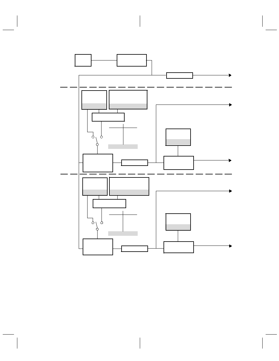
23
See Table 2-3
See Table 2-3
See Table 2-3
See Table 2-3
7.20 kHz for RB = 40
8.00 kHz for RB = 36
9.60 kHz for RB = 30
14.4 kHz for RB = 20
16.0 kHz for RB = 18
19.2 kHz for RB = 15
7.20 kHz for TB = 40
8.00 kHz for TB = 36
9.60 kHz for TB = 30
14.4 kHz for TB = 20
16.0 kHz for TB = 18
19.2 kHz for TB = 15
Divide By 2
XTAL
OSC
20.736 MHZ
41.472 MHZ
TA Register
(5 Bits)
Divide By 2
576 kHz
TB Register
(6 Bits)
RA Register
(5 Bits)
576 kHz
Divide By 4
1.296 MHz
2.592 MHz
5.184 MHz
10.368 MHz
MASTER CLOCK
TMS320 DSP
SHIFT CLOCK
TA
REGISTER
(6 Bits)
2s-Complement TA
Adder/Subtractor
D1 D0 SELECT
0
0
1
1
0
1
0
1
TA
TA + TA
TA TA
TA
See Table 2-2
TX (A) Counter
(6 Bits)
TX (B) Counter
288 kHz
SCF CLOCK
Low-Pass Filter,
(sin x)/x Filter
D/A Conversion
Frequency
See Table 2-3
RA
Register
(6 Bits)
2s-Complement RA
See Table 2-3
Adder/Subtractor
RX (A) Counter
(6 Bits)
D1 D0 SELECT
0
0
1
1
0
1
0
1
RA
RA + RA
RA RA
RA
See Table 2-2
RB Register
(6 Bits)
RX (B) Counter
High-Pass Filter,
A/D Conversion
Frequency
288 kHz
Low-Pass Filter
SCF CLOCK
9
18
9
18
Transmit Section
D/A Conversion
Timing
Receive Section
A/D Conversion
Timing
These control bits are described in the DX Serial Data Word Format section.
NOTES: A. Tables 22 and 23 are primary and secondary communication protocols, respectively.
B. In synchronous operation, RA, RA', RB, RX(A), and RX(B) are not used. TA, TA', TB, TX(A), and TX(B) are
used instead.
C. Items in italics refer only to frequencies and register contents, which are variable. A crystal oscillator driving
20.736 MHz into the TMS320-series DSP provides a master clock frequency of 5.184 MHz. The TLC32046
produces a shift clock frequency of 1.296 MHz. If the TX(A) register contents equal 9, the SCF clock
frequency is 288 kHz, and the D/A conversion frequency is 288 kHz
÷
T(B).
Figure 21. Asynchronous Internal Timing Configuration

24
2.2
Analog Input
Two pairs of analog inputs are provided. Normally, the IN+ and IN input pair is used; however, the auxiliary
input pair, AUX IN+ and AUX IN, can be used if a second input is required. Since sufficient common-mode
range and rejection are provided, each input set can be operated in differential or single-ended modes. The
gain for the IN +, IN , AUX IN +, and AUX IN inputs can be programmed to 1, 2, or 4 (see Table 4 1). Either
input circuit can be selected via software control. Multiplexing is controlled with the D4 bit (enable/disable
AUX IN+ and AUX IN ) of the secondary DX word (see Table 23). The multiplexing requires a 2-ms wait
at SCF = 288 kHz (see Figure 53) for a valid output signal. A wide dynamic range is ensured by the
differential internal analog architecture and the separate analog and digital voltage supplies and grounds.
2.3
A/D Band-Pass Filter, Clocking, and Conversion Timing
The receive-channel A/D high-pass filter can be selected or bypassed via software control (see Functional
Block Diagram). The frequency response of this filter is found in the electrical characteristic section. This
response results when the switched-capacitor filter clock frequency is 288 kHz and the A/D sample rate is
16 kHz. Several possible options can be used to attain a 288-kHz switched-capacitor filter clock. When the
filter clock frequency is not 288 kHz, the low-pass filter transfer function is frequency-scaled by the ratio of
the actual clock frequency to 288 kHz (see Typical Characteristics section). The ripple bandwidth and 3-dB
low-frequency roll-off points of the high-pass section are 300 Hz and 200 Hz, respectively. However, the
high-pass section low-frequency roll-off is frequency-scaled by the ratio of the A/D sample rate to 16 kHz.
Figure 21 and the DX serial data word format sections of this data manual indicate the many options for
attaining a 288-kHz band-pass switched-capacitor filter clock. These sections indicate that the RX(A)
counter can be programmed to give a 288-kHz band-pass switched-capacitor filter clock for several master
clock input frequencies.
The A/D conversion rate is attained by frequency-dividing the band-pass switched-capacitor filter clock with
the RX(B) counter. Unwanted aliasing is prevented because the A/D conversion rate is an integer
submultiple of the band-pass switched-capacitor filter sampling rate, and the two rates are synchronously
locked.
2.4
A/D Converter
Fundamental performance specifications for the receive channel ADC circuitry are in the electrical
characteristic section of this data manual. The ADC circuitry, using switched-capacitor techniques, provides
an inherent sample-and-hold function.
2.5
Analog Output
The analog output circuitry is an analog output power amplifier. Both noninverting and inverting amplifier
outputs are brought out of the IC. This amplifier can drive transformer hybrids or low-impedance loads
directly in either a differential or single-ended configuration.
2.6
D/A Low-Pass Filter, Clocking, and Conversion Timing
The frequency response results when the low-pass switched-capacitor filter clock frequency is 288 kHz (see
equation 1). Like the A/D filter, the transfer function of this filter is frequency-scaled when the clock frequency
is not 288 kHz (see Typical Characteristics section). A continuous-time filter is provided on the output of the
low-pass filter to eliminate the periodic sample data signal information, which occurs at multiples of the
288-kHz switched-capacitor clock feedthrough.
The D/A conversion rate is attained by frequency-dividing the 288-kHz switched-capacitor filter clock with
the T(B) counter. Unwanted aliasing is prevented because the D/A conversion rate is an integer submultiple
of the switched-capacitor low-pass filter sampling rate, and the two rates are synchronously locked.
2.7
D/A Converter
Fundamental performance specifications for the transmit channel DAC circuitry are in the electrical
characteristic section. The DAC has a sample-and-hold function that is realized with a switched-capacitor
ladder.

25
2.8
Serial Port
The serial port has four possible configurations summarized in the function table on page 12. These
configurations are briefly described below.
·
The transmit and receive sections are operated asynchronously, and the serial port interfaces
directly with the TMS320C17. The communications protocol is two 8-bit bytes.
·
The transmit and receive sections are operated asynchronously, and the serial port interfaces
directly with the TMS32020, TMS320C25, and TMS320C30. The communications protocol is
one 16-bit word.
·
The transmit and receive sections are operated synchronously, and the serial port interfaces
directly with the TMS320C17. The communications protocol is two 8-bit bytes.
·
The transmit and receive sections are operated synchronously, and the serial port interfaces
directly with the TMS32020, TMS320C25, TMS320C30, or two SN74299 serial-to-parallel shift
registers, which can interface in parallel to the TMS32010, TMS320C15, to any other digital
signal processor, or to external FIFO circuitry. The communications protocol is one 16-bit word.
2.9
Synchronous Operation
When the transmit and receive sections are operated synchronously, the low-pass filter clock drives both
low-pass and band-pass filters (see Functional Block Diagram). The A/D conversion timing is derived from
and equal to the D/A conversion timing. When data bit D5 in the control register is a logic 1, transmit and
receive sections are synchronous. The band-pass switched-capacitor filter and the A/D converter timing are
derived from the TX(A) counter, the TX(B) counter, and the TA and TA' registers. In synchronous operation,
both the A/D and the D/A channels operate from the same frequencies. The FSX and the FSR timing is
identical during primary communication, but FSR is not asserted during secondary communication because
there is no new A/D conversion result.
2.9.1
One 16-Bit Word (Dual-Word [ Telephone Interface] or Word Mode)
The serial port interfaces directly with the serial ports of the TMS32020, TMS320C25, and the TMS320C30,
and communicates in one 16-bit word. The operation sequence is as follows:
1.
The FSX and FSR pins are brought low by the TLC32046 AIC.
2.
One 16-bit word is transmitted and one 16-bit word is received.
3.
FSX and FSR are brought high.
4.
EODX and EODR emit low-going pulses one shift clock wide. EODX and EODR are valid in the
word or byte mode only.
If the device is in the dual-word (telephone interface) mode, FSD goes low during the secondary
communication period and enables the data word received at the DATA-DR/CONTROL input to be routed
to the DR line. The secondary communication period occurs four shift clocks after completion of primary
communications.
2.9.2
Two 8-Bit Bytes (Byte Mode)
The serial port interfaces directly with the serial port of the TMS320C17 and communicates in two 8-bit
bytes. The operation sequence is as follows:
1.
FSX and FSR are brought low.
2.
One 8-bit word is transmitted and one 8-bit word is received.
3.
EODX and EODR are brought low.
4.
FSX and FSR emit positive frame-sync pulses that are four shift clock cycles wide.
5.
One 8-bit byte is transmitted and one 8-bit byte is received.
6.
FSX and FSR are brought high.
7.
EODX and EODR are brought high.

26
2.9.3
Synchronous Operating Frequencies
The synchronous operating frequencies are determined by the following equations.
Switched capacitor filter (SCF) frequencies (see Figure 21):
Low-pass SCF clock frequency
(D A and A D channels)
+
master clock frequency
T(A)
2
High-pass SCF clock frequency (A D channel)
+
A D conversion frequency
Conversion frequency (A D and D A channels)
+
low-pass SCF clock frequency
T(B)
+
master clock frequency
T(A)
2
T(B)
NOTE: T(A), T(B), R(A), and R(B) are the contents of the TA, TB, RA, and RB registers, respectively.
2.10 Asynchronous Operation
When the transmit and the receive sections are operated asynchronously, the low-pass and band-pass filter
clocks are independently generated from the master clock. The D/A and the A/D conversion timing is also
determined independently.
D/A timing is set by the counters and registers described in synchronous operation, but the RA and RB
registers are substituted for the TA and TB registers to determine the A/D channel sample rate and the A/D
path switched-capacitor filter frequencies. Asynchronous operation is selected by control register bit D5
being zero.
2.10.1
One 16-Bit Word (Word Mode)
The serial port interfaces directly with the serial ports of the TMS32020, TMS320C25, and TMS320C30 and
communicates with 16-bit word formats. The operation sequence is as follows:
1.
FSX or FSR are brought low by the TLC32046 AIC.
2.
One 16-bit word is transmitted or one 16-bit word is received.
3.
FSX or FSR are brought high.
4.
EODX or EODR emit low-going pulses one shift clock wide. EODX and EODR are valid in either
the word or byte mode only.
2.10.2
Two 8-Bit Bytes (Byte Mode)
The serial port interfaces directly with the serial port of the TMS320C17 and communicates in two 8-bit
bytes. The operating sequence is as follows:
1.
FSX or FSR are brought low by the TLC32046 AIC.
2.
One byte is transmitted or received.
3.
EODX or EODR are brought low.
4.
FSX or FSR are brought high for four shift clock periods and then brought low.
5.
The second byte is transmitted or received.
6.
FSX or FSR are brought high.
7.
EODX or EODR are brought high.
2.10.3
Asynchronous Operating Frequencies
The asynchronous operating frequencies are determined by the following equations.
Switched-capacitor filter frequencies (see Figure 21):
Low-pass D A SCF clock frequency
+
master clock frequency
T(A)
2

27
Low-pass A D SCF clock frequency
+
master clock frequency
R(A)
2
High-pass SCF clock frequency (A D channel)
+
A D conversion frequency
(2)
Conversion frequency:
D A conversion frequency
+
low-pass D A SCF clock frequency
T(B)
A D conversion frequency
+
low-pass A D SCF clock frequency (for low pass receive filter)
R(B)
-
(3)
NOTE: T(A), T(B), R(A), and R(B) are the contents of the TA, TB, RA, and RB registers, respectively.
2.11 Operation of TLC32046 With Internal Voltage Reference
The internal reference of the TLC32046 eliminates the need for an external voltage reference and provides
overall circuit cost reduction. The internal reference eases the design task and provides complete control
of the IC performance. The internal reference is brought out to REF. To keep the amount of noise on the
reference signal to a minimum, an external capacitor can be connected between REF and ANLG GND.
2.12 Operation of TLC32046 With External Voltage Reference
REF can be driven from an external reference circuit. This external circuit must be capable of supplying
250
µ
A and must be protected adequately from noise and crosstalk from the analog input.
2.13 Reset
A reset function is provided to initiate serial communications between the AIC and DSP and to allow fast,
cost-effective testing during manufacturing. The reset function initializes all AIC registers, including the
control register. After a negative-going pulse on RESET, the AIC is initialized. This initialization allows
normal serial port communications activity to occur between AIC and DSP (see AIC DX Data Word Format
section). After RESET, TA=TB=RA=RB=18 (or 12 hexadecimal), TA
=RA
=01 (hexadecimal), the A/D
high-pass filter is inserted, the loop-back function is deleted, AUX IN+ and AUX IN are disabled, transmit
and receive sections are in synchronous operation, programmable gain is set to 1, the on-board (sin x)/x
correction filter is not selected, D10OUT is set to 0, and D11OUT is set to 0.
2.14 Loopback
This feature allows the circuit to be tested remotely. In loopback, OUT+ and OUT are internally connected
to IN+ and IN . The DAC bits (D15 to D2), which are transmitted to DX, can be compared with the ADC bits
(D15 to D2), received from DR. The bits on DR equal the bits on DX. However, there is some difference in
these bits due to the ADC and DAC output offsets.
The loopback feature is implemented with digital signal processor control by transmitting a logic 1 for data
bit D3 in the DX secondary communication to the control register (see Table 23).
28
2.15 Communications Word Sequence
In the dual-word (telephone interface) mode, there are two data words that are presented to the DSP or
µ
P
from the DR terminal. The first data word is the ADC conversion result occurring during the FSR time, and
the second is the serial data applied to DATA-DR during the FSD time. FSR is not asserted during secondary
communications and FSD is not asserted during primary communications.
DX-14 Bits Digital 11
From DSP to DAC
4 Shift
Clocks
DX-14 Bits Digital XX
From DSP
Input for D/A
Conversion
Input for Register
Program
2s Complement Output
From ADC to the DSP
2s Complement Output
From ADC to the DSP
Data From DATA-DR
to the DSP
16 bits
16 bits
Primary
Communications
Secondary
Communications
FSX
DX
FSR
DR
TLC32046
TLC32046
TLC32046
Dual-Word
(telephone interface)
Mode Only
TLC32046
Dual-Word
(telephone interface)
Mode Only
16 bits Digital From
DATA-DR to DR
FSD
TLC32046
Dual-Word
(telephone interface)
Mode Only
Figure 22. Primary and Secondary Communications Word Sequence
2.15.1
DR Word Bit Pattern
The data word is the 14-bit conversion result of the receive channel to the processor in 2s complement
format. With 16-bit processors, the data is 16 bits long with the two LSBs at zero.
A/D MSB
1st bit sent
A/D LSB
D15
D14
D13
D12
D11
D10
D9
D8
D7
D6
D5
D4
D3
D2
D1
D0
29
2.15.2
Primary DX Word Bit Pattern
Using 8-bit processors, the data word is transmitted in the same order as one 16-bit word, but as two bytes
with the two LSBs of the second byte set to zero.
A/D OR D/A MSB
1st bit sent
1st bit sent of 2nd byte
A/D or D/A LSB
D15
D14
D13
D12
D11
D10
D9
D8
D7
D6
D5
D4
D3
D2
D1
D0
Table 22. Primary DX Serial Communication Protocol
FUNCTIONS
D1
D0
D15 (MSB)-D2
DAC Register.
TA
TX(A), RA
RX(A) (see Figure 21).
TB
TX(B), RB
RX(B) (see Figure 21).
0
0
D15 (MSB)-D2
DAC Register.
TA+TA
TX(A), RA+RA
RX(A) (see Figure 21).
TB
TX(B), RB
RX(B) (see Figure 21).
The next D/A and A/D conversion period is changed by the addition of TA
and RA
master clock cycles,
in which TA
and RA
can be positive, negative, or zero (refer to Table 24).
0
1
D15 (MSB)-D2
DAC Register.
TATA
TX(A), RARA
RX(A) (see Figure 21).
TB
TX(B), RB
RX(B) (see Figure 21).
The next D/A and A/D conversion period is changed by the subtraction of TA
and RA
master clock cycles,
in which TA
and RA
can be positive, negative, or zero (refer to Table 24).
1
0
D15 (MSB)-D2
DAC Register.
TA
TX(A), RA
RX(A) (see Figure 21).
TB
TX(B), RB
RX(B) (see Figure 21).
After a delay of four shift cycles, a secondary transmission follows to program the AIC to operate in the
desired configuration. In the telephone interface mode, data on DATA DR is routed to DR during
secondary transmission.
1
1
NOTE: Setting the two least significant bits to 1 in the normal transmission of DAC information (primary communications)
to the AIC initiates secondary communications upon completion of the primary communications. When the
primary communication is complete, FSX remains high for four SHIFT CLOCK cycles and then goes low and
initiates the secondary communication. The timing specifications for the primary and secondary communications
are identical. In this manner, the secondary communication, if initiated, is interleaved between successive
primary communications. This interleaving prevents the secondary communication from interfering with the
primary communications and DAC timing. This prevents the AIC from skipping a DAC output. FSR is not asserted
during secondary communications activity. However, in the dual-word (telephone
interface) mode, FSD is
asserted during secondary communications but not during primary communications.
210
2.15.3
Secondary DX Word Bit Pattern
D/A MSB
1st bit sent
1st bit sent of 2nd byte
D/A LSB
D15
D14
D13
D12
D11
D10
D9
D8
D7
D6
D5
D4
D3
D2
D1
D0
Table 23. Secondary DX Serial Communication Protocol
FUNCTIONS
D1
D0
D13 (MSB)-D9
TA , 5 bits unsigned binary (see Figure 21).
D6 (MSB)-D2
RA, 5 bits unsigned binary (see Figure 21).
D15, D14, D8, and D7 are unassigned.
0
0
D14 (sign bit)-D9
TA
, 6 bits 2s complement (see Figure 21).
D7 (sign bit)-D2
RA
, 6 bits 2s complement (see Figure 21).
D15 and D8 are unassigned.
0
1
D14 (MSB)-D9
TB, 6 bits unsigned binary (see Figure 21).
D7 (MSB)-D2
RB, 6 bits unsigned binary (see Figure 21).
D15 and D8 are unassigned.
1
0
D2 = 0/1 deletes/inserts the A/D high-pass filter.
D3 = 0/1 deletes/inserts the loopback function.
D4 = 0/1 disables/enables AUX IN+ and AUX IN.
D5 = 0/1 asynchronous/synchronous transmit and receive sections.
D6 = 0/1 gain control bits (see Table 41).
D7 = 0/1 gain control bits (see Table 41).
D9 = 0/1 delete/insert on-board second-order (sinx)/x correction filter
D10 = 0/1 output to D10OUT (dual-word (telephone interface) mode)
D11 = 0/1 output to D11OUT (dual-word (telephone interface) mode)
D8, D12D15 are unassigned.
1
1
2.16 Reset Function
A reset function is provided to initiate serial communications between the AIC and DSP. The reset function
initializes all AIC registers, including the control register. After power has been applied to the AIC, a
negative-going pulse on RESET initializes the AIC registers to provide a 16-kHz A/D and D/A conversion
rate for a 10.368-MHz master clock input signal. Also, the pass-bands of the A/D and D/A filters are 300
Hz to 7200 Hz and 0 Hz to 7200 Hz, respectively; therefore, the filter bandwidths are half those shown in
the filter transfer function specification section. The AIC, except the CONTROL register, is initialized as
follows (see AIC DX Data Word Format section):
REGISTER
INITIALIZED VALUE (HEX)
TA
12
TA
01
TB
12
RA
12
RA
01
RB
12
The CONTROL register bits are reset as follows (see Table 23):
D11 = 0, D10 = 0, D9 = 1, D7 = 1, D6 = 1, D5 = 1, D4 = 0, D3 = 0, D2 = 1
This initialization allows normal serial port communications to occur between the AIC and the DSP. If the
transmit and receive sections are configured to operate synchronously and the user wishes to program
different conversion rates, only the TA, TA
, and TB register need to be programmed. Both transmit and
receive timing are synchronously derived from these registers (see the Terminal Functions and DX Serial
Data Word Format sections).
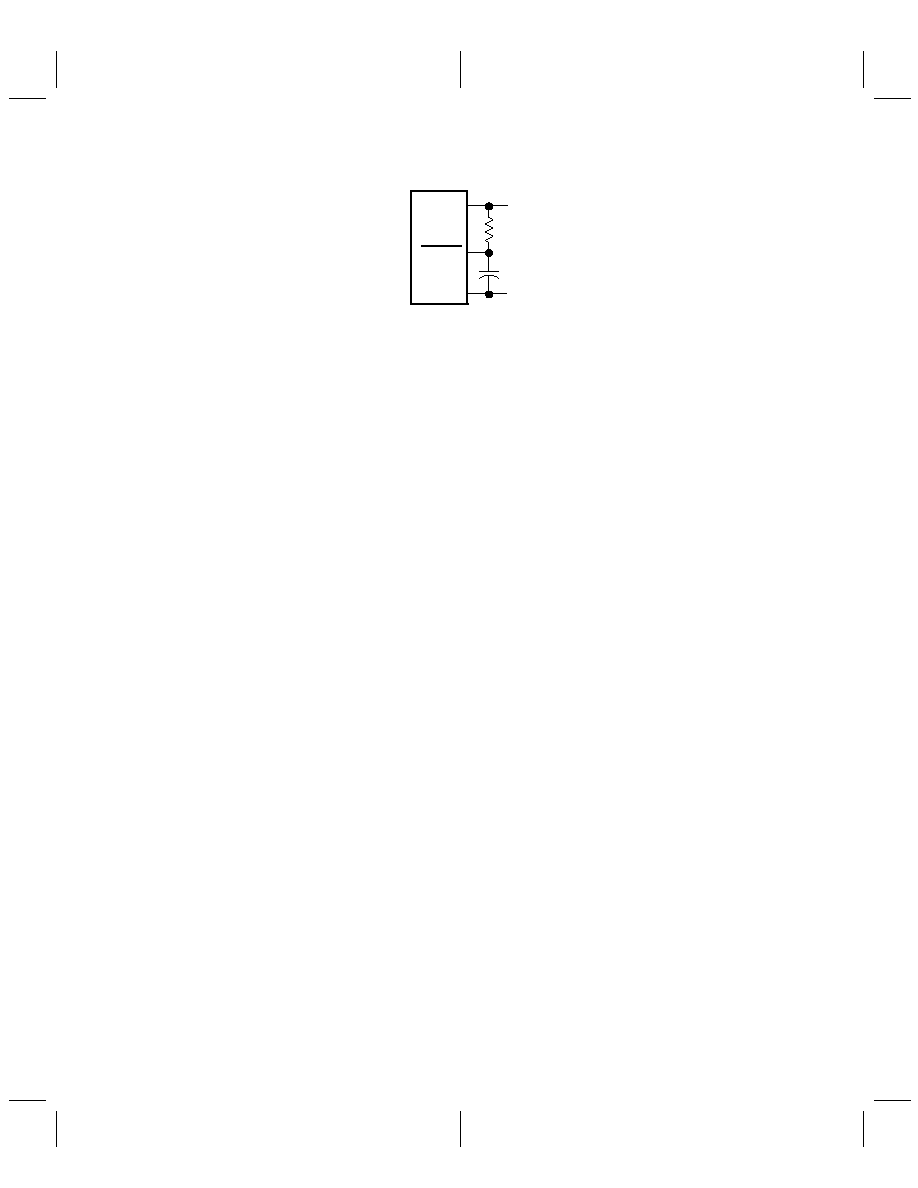
Figure 23 shows a circuit that provides a reset on power-up when power is applied in the sequence given
in the power-up sequence section. The circuit depends on the power supplies reaching their recommended
values a minimum of 800 ns before the capacitor charges to 0.8 V above DGTL GND.
211
VCC +
RESET
VCC
200 k
5 V
0.5
µ
F
5 V
TLC32046
Figure 23. Reset on Power-Up Circuit
2.17 Power-Up Sequence
To ensure proper operation of the AIC and as a safeguard against latch-up, it is recommended that Schottky
diodes with forward voltages less than or equal to 0.4 V be connected from V
CC
to ANLG GND and from
V
CC
to DGTL GND. In the absence of such diodes, power is applied in the following sequence: ANLG GND
and DGTL GND, V
CC
, then V
CC+
and V
DD
. Also, no input signal is applied until after power-up.
2.18 AIC Register Constraints
The following constraints are placed on the contents of the AIC registers:
1.
TA register must be
4 in word mode (WORD/BYTE= high).
2.
TA register must be
5 in byte mode (WORD/BYTE= low).
3.
TA
register can be either positive, negative, or zero.
4.
RA register must be
4 in word mode (WORD/BYTE = high).
5.
RA register must be
5 in byte mode (WORD/BYTE = low).
6.
RA
register can be either positive, negative, or zero.
7.
(TA register
±
TA
register) must be > 1.
8.
(RA register
±
RA
register) must be > 1.
9.
TB register must be
15.
10. RB register must be
15.
2.19 AIC Responses to Improper Conditions
The AIC has provisions for responding to improper conditions. These improper conditions and the response
of the AIC to these conditions are presented in Table 2 4.
212
Table 24. AIC Responses to Improper Conditions
IMPROPER CONDITION
AIC RESPONSE
TA register + TA
register = 0 or 1
Reprogram TX(A) counter with TA register value
g
g
TA register TA
register = 0 or 1
g
( )
g
TA register + TA
register < 0
MODULO 64 arithmetic is used to ensure that a positive value is loaded into
TX(A) counter, i.e., TA register + TA
register + 40 HEX is loaded into TX(A)
counter.
RA register + RA
register = 0 or 1
Reprogram RX(A) counter with RA register value
g
g
RA register RA
register = 0 or 1
g
( )
g
RA register + RA
register = 0 or 1
MODULO 64 arithmetic is used to ensure that a positive value is loaded into
RX(A) counter, i.e., RA register + RA
register + 40 HEX is loaded into RX(A)
counter.
TA register = 0 or 1
AIC is shut down. Reprogram TA or RA registers after a reset.
g
RA register = 0 or 1
g
g
TA register < 4 in word mode
The AIC serial port no longer operates. Reprogram TA or RA registers after
g
TA register < 5 in byte mode
g
g
g
a reset.
RA register < 4 in word mode
RA
i t
5 i b t
d
RA register < 5 in byte mode
TB register < 15
Reprogram TB register with 12 HEX
RB register < 15
Reprogram RB register with 12 HEX
AIC and DSP cannot communicate
Hold last DAC output
2.20 Operation With Conversion Times Too Close Together
If the difference between two successive D/A conversion frame syncs is less than 1/25 kHz, the AIC
operates improperly. In this situation, the second D/A conversion frame sync occurs too quickly, and there
is not enough time for the ongoing conversion to be completed. This situation can occur if the A and B
registers are improperly programmed or if the A + A
register result is too small. When incrementally
adjusting the conversion period via the A + A
register options, the designer should not violate this
requirement (see Figure 24).
t2 t1
1/25 kHz
t2
t1
Ongoing Conversion
Frame Sync
(FSX or FSR)
Figure 24. Conversion Times Too Close Together
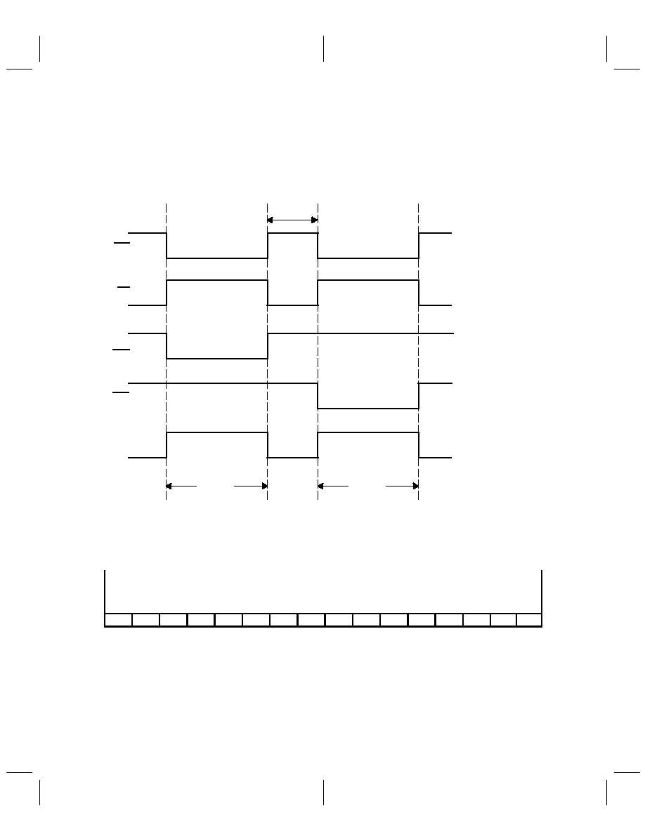
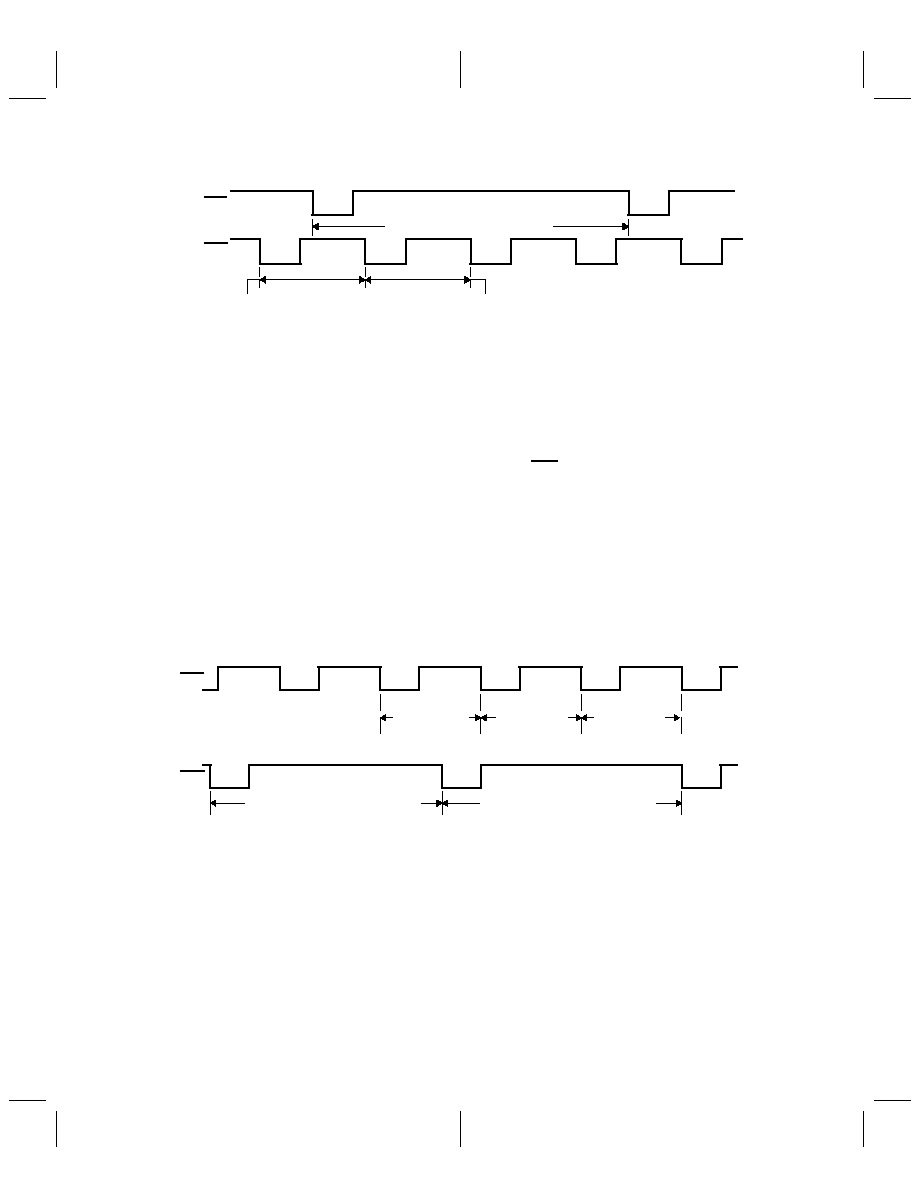
2.21 More Than One Receive Frame Sync Occurring Between Two Transmit
Frame Syncs Asynchronous Operation
When incrementally adjusting the conversion period via the A + A
or A A
register options, a specific
protocol is followed. The command to use the incremental conversion period adjust option is sent to the AIC
during an FSX frame sync. The ongoing conversion period is then adjusted; however, either receive
conversion period A or conversion period B can be adjusted. For both transmit and receive conversion
periods, the incremental conversion period adjustment is performed near the end of the conversion period.
If there is sufficient time between t
1
and t
2
, the receive conversion period adjustment is performed during
receive conversion period A. Otherwise, the adjustment is performed during receive conversion period B.
The adjustment command only adjusts one transmit conversion period and one receive conversion period.
To adjust another pair of transmit and receive conversion periods, another command must be issued during
a subsequent FSX frame (see Figure 25).
213
FSR
FSX
Period A
Receive Conversion
Transmit Conversion Period
t1
Period B
Receive Conversion
Figure 25. More Than One Receive Frame Sync Between Two Transmit Frame Syncs
2.22 More Than One Transmit Frame Sync Occurring Between Two Receive
Frame Syncs Asynchronous Operation
When incrementally adjusting the conversion period via the A + A
or A A
register options, a specific
protocol must be followed. For both transmit and receive conversion periods, the incremental conversion
period adjustment is performed near the end of the conversion period. The command to use the incremental
conversion period adjust options is sent to the AIC during an FSX frame sync. The ongoing transmit
conversion period is then adjusted. However, three possibilities exist for the receive conversion period
adjustment as shown in Figure 26. When the adjustment command is issued during transmit conversion
period A, receive conversion period A is adjusted if there is sufficient time between t
1
and t
2
. If there is not
sufficient time between t
1
and t
2
, receive conversion period B is adjusted. The third option is that the receive
portion of an adjustment command can be ignored if the adjustment command is sent during a receive
conversion period, which is adjusted due to a prior adjustment command. For example, if adjustment
commands are issued during transmit conversion periods A, B, and C, the first two commands may cause
receive conversion periods A and B to be adjusted, while the third receive adjustment command is ignored.
The third adjustment command is ignored since it was issued during receive conversion period B, which
already is adjusted via the transmit conversion period B adjustment command.
FSR
FSX
Receive Conversion Period B
Receive Conversion Period A
t2
t1
Period C
Conversion
Transmit
Period B
Conversion
Transmit
Period A
Conversion
Transmit
Figure 26. More Than One Transmit Frame Sync Between Two Receive Frame Syncs
2.23 More than One Set of Primary and Secondary DX Serial Communications
Occurring Between Two Receive Frame Syncs (See DX Serial Data Word
Format section) Asynchronous Operation
The TA, TA
, TB, and control register information that is transmitted in the secondary communication is
accepted and applied during the ongoing transmit conversion period. If there is sufficient time between t
1
and t
2
, the TA, RA
, and RB register information, sent during transmit conversion period A, is applied to
receive conversion period A; otherwise, this information is applied during receive conversion period B. If RA,
RA
, and RB register information has been received and is being applied during an ongoing conversion
period, any subsequent RA, RA
, or RB information received during this receive conversion period is
disregarded (see Figure 27).
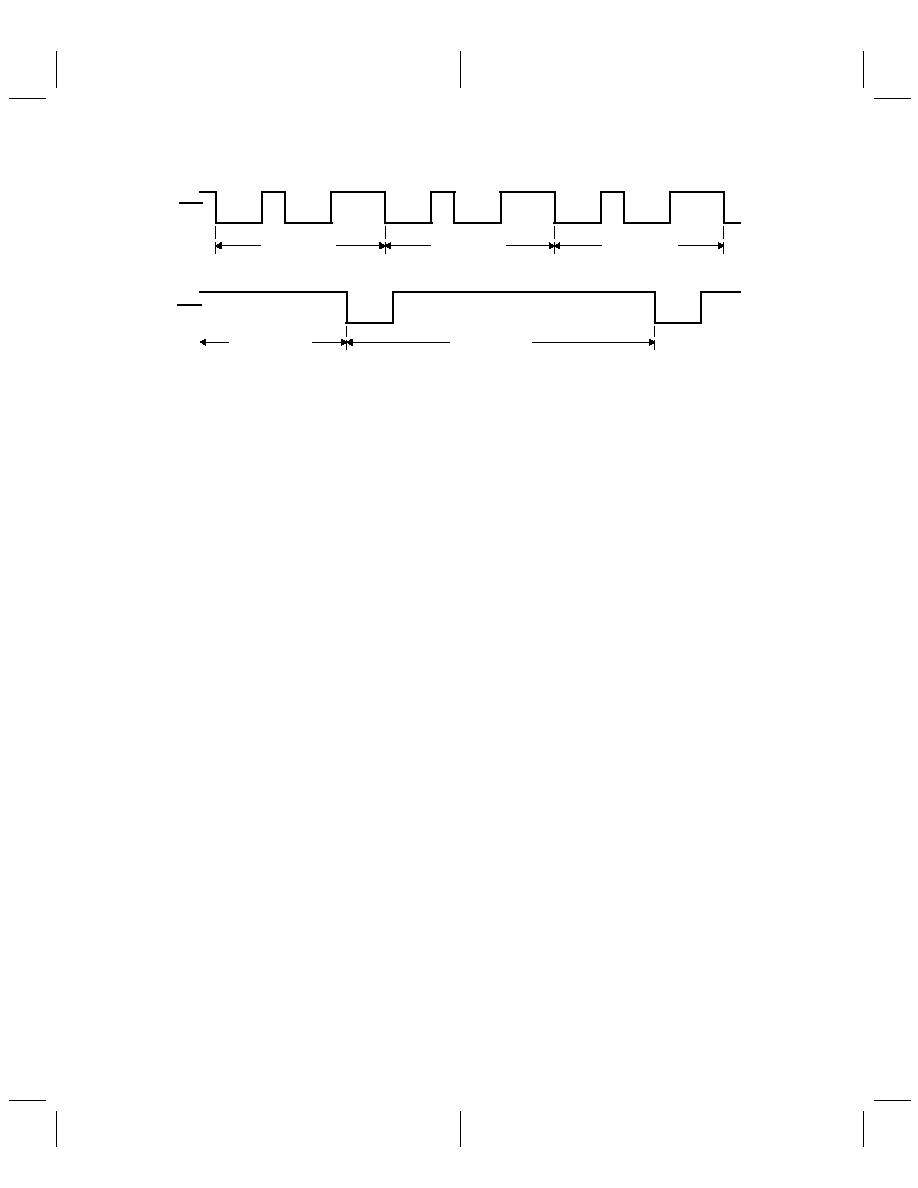
214
FSR
FSX
t2
Secondary
Primary
Secondary
Primary
t1
Secondary
Primary
Transmit
Conversion
Preload A
Transmit
Conversion
Preload B
Transmit
Conversion
Preload C
Receive
Conversion
Period A
Receive
Conversion
Period B
Figure 27. More Than One Set of Primary and Secondary DX
Serial Communications Between Two Receive Frame Syncs
2.24 System Frequency Response Correction
The (sin x)/x correction for the DAC zero-order sample-and-hold output can be provided by an on-board
second-order (sin x)/x correction filter (see Functional Block Diagram). This (sin x)/x correction filter can be
inserted into or omitted from the signal path by digital-signal-processor control (data bit D9 in the DX
secondary communications). When inserted, the (sin x)/x correction filter precedes the switched-capacitor
low-pass filter. When the TB register (see Figure 21) equals 15, the correction results of Figures 5 5, 5 6,
and 5 7 can be obtained.
The (sin x)/x correction [see section (sin x)/x] can also be accomplished by disabling the on-board
second-order correction filter and performing the (sin x)/x correction in digital signal processor software. The
system frequency response can be corrected via DSP software to
±
0.1 dB accuracy to a band edge of
3000 Hz for all sampling rates. This correction is accomplished with a first-order digital correction filter, that
requires seven TMS320 instruction cycles. With a 200-ns instruction cycle, seven instructions represent an
overhead factor of 1.1% and 1.3% for sampling rates of 8 and 9.6 kHz, respectively (see the (Sin x)/x
Correction Section for more details).
2.25 (Sin x)/x Correction
If the designer does not wish to use the on-board second-order (sin x)/x correction filter, correction can be
accomplished in digital signal processor (DSP) software. (Sin x)/x correction can be accomplished easily
and efficiently in digital signal processor software. Excellent correction accuracy can be achieved to a band
edge of 3000 Hz by using a first-order digital correction filter. The results shown are typical of the numerical
correction accuracy that can be achieved for sample rates of interest. The filter requires seven instruction
cycles per sample on the TMS320 DS. With a 200-ns instruction cycle, nine instructions per sample
represents an overhead factor of 1.4% and 1.7% for sampling rates of 8000 Hz and 9600 Hz, respectively.
This correction adds a slight amount of group delay at the upper edge of the 300-Hz to 3000-Hz band.
2.26 (Sin x)/x Roll-Off for a Zero-Order Hold Function
The (sin x)/x roll-off error for the AIC DAC zero-order hold function at a band-edge frequency of 3000 Hz
for the various sampling rates is shown in Table 25 (see Figure 5 7).
Error = 20 log
sin
f/fs
f/fs
215
Table 25. (sin x)/x Roll-Off Error
fs (Hz)
f = 3000 Hz
f = 3000 Hz
(dB)
7200
2.64
8000
2.11
9600
1.44
14400
0.63
16000
0.50
19200
0.35
25000
0.21
The actual AIC (sin x)/x roll-off is slightly less than the figures in Table 25 because the AIC has less than
100% duty cycle hold interval.
2.27 Correction Filter
To externally compensate for the (sin x)/x roll-off of the AIC, a first-order correction filter can be implemented
as shown in Figure 28.
y(i + 1)
p1
+
+
(1 p1) p2
u (i + 1)
Z 1
X
X
Figure 28. First-Order Correction Filter
The difference equation for this correction filter is:
(4)
y
(i + 1)
= p2
(1 p1)
u
(i + 1)
+ p1
y
(i)
where the constant p1 determines the pole locations.
The resulting squared magnitude transfer function is:
|
H (f)
|
2
=
(p2)
2
V
(1p1)
2
1 2
V
p1
V
cos (2
p
f/f
s
) + (p1)
2
(5)
2.28 Correction Results
Table 2-6 shows the optimum p values and the corresponding correction results for 8000-Hz and 9600-Hz
sampling rates (see Figures 5 8, 5 9, and 5 10).
216
Table 26. (Sin x)/x Correction Table for f
s
= 8000 Hz and f
s
= 9600 Hz
ROLL-OFF ERROR (dB)
ROLL-OFF ERROR (dB)
f (Hz)
ROLL OFF ERROR (dB)
fs = 8000 Hz
ROLL OFF ERROR (dB)
fs = 9600 Hz
f (Hz)
s
p1 = 0.14813
s
p1 = 0.1307
p2 = 0.9888
p2 = 0.9951
300
0.099
0.043
600
0.089
0.043
900
0.054
0
1200
0.002
0
1500
0.041
0
1800
0.079
0.043
2100
0.100
0.043
2400
0.091
0.043
2700
0.043
0
3000
0.102
0.043
2.29 TMS320 Software Requirements
The digital correction filter equation can be written in state variable form as follows:
y
(i+1)
= y
(i)
k1
+ u
(i+1)
k2
Where
k1 = p1
k2 = (1 p1) p2
y(i) = filter state
u(i+1) = next I/O sample
The coefficients k1 and k2 must be represented as 16-bit integers. The SACH instruction (with the proper
shift) yields the correct result. With the assumption that the TMS320 processor page pointer and memory
configuration are properly initialized, the equation can be executed in seven instructions or seven cycles
with the following program:
ZAC
LT K2
MPY U
LTA K1
MPY Y
APAC
SACH (dma), (shift)
31
3
Specifications
3.1
Absolute Maximum Ratings Over Operating Free-Air Temperature Range
(Unless Otherwise Noted)
Supply voltage range, V
CC+
(see Note 1)
0.3 V to 15 V
. . . . . . . . . . . . . . . . . . . . . . . . . .
Supply voltage range, V
DD
0.3 V to 15 V
. . . . . . . . . . . . . . . . . . . . . . . . . . . . . . . . . . . . . . .
Output voltage range, V
O
0.3 V to 15 V
. . . . . . . . . . . . . . . . . . . . . . . . . . . . . . . . . . . . . . . .
Input voltage range, V
I
0.3 V to 15 V
. . . . . . . . . . . . . . . . . . . . . . . . . . . . . . . . . . . . . . . . . . .
Digital ground voltage range
0.3 V to 15 V
. . . . . . . . . . . . . . . . . . . . . . . . . . . . . . . . . . . . . .
Operating free-air temperature range: TLC32046C
0
°
C to 70
°
C
. . . . . . . . . . . . . . . . . . .
TLC32046I
40
°
C to 85
°
C
. . . . . . . . . . . . . . . . . .
TLC32046M
55
°
C to 125
°
C
. . . . . . . . . . . . . . . .
Storage temperature range: TLC32046C, TLC32046I
40
°
C to 125
°
C
. . . . . . . . . . . . .
TLC32046M
65
°
C to 150
°
C
. . . . . . . . . . . . . . . . . . . . . . . .
Case temperature for 10 seconds: FN or FK package
260
°
C
. . . . . . . . . . . . . . . . . . . . . . .
Lead temperature 1,6 mm (1/16 inch) from case for 10 seconds:
N or J package
260
°
C
. . . . . . . . . . . . . . . . . . . . . . . . . . . . . . . . . . . . . . . . . . . . . . . . . . . .
NOTE 1: Voltage values for maximum ratings are with respect to VCC .
3.2
Recommended Operating Conditions
MIN
NOM
MAX
UNIT
Supply voltage, VCC+ (see Note 2)
4.75
5
5.25
V
Supply voltage, VCC (see Note 2)
4.75
5
5.25
V
Digital supply voltage, VDD (see Note 2)
4.75
5
5.25
V
Digital ground voltage with respect to ANLG GND, DGTL GND
0
V
Reference input voltage, Vref(ext) (see Note 2)
2
4
V
High-level input voltage, VIH
2
VDD+0.3
V
Low-level input voltage, VIL (see Note 3)
0.3
0.8
V
Load resistance at OUT+ and/or OUT, RL
300
Load capacitance at OUT+ and/or OUT, CL
100
pF
MSTR CLK frequency (see Note 4)
5
10.368
MHz
Analog input amplifier common mode input voltage (see Note 5)
±
1.5
V
A/D or D/A conversion rate
25
kHz
TLC32046C
0
70
Operating free-air temperature range, TA
TLC32046I
40
85
°
C
g
g
A
TLC32046M
55
125
NOTES:
2. Voltages at analog inputs and outputs, REF, VCC+, and VCC are with respect to ANLG GND. Voltages at
digital inputs and outputs and VDD are with respect to DGTL GND.
3. The algebraic convention, in which the least positive (most negative) value is designated minimum, is used
in this data manual for logic voltage levels only.
4. The band-pass switched-capacitor filter (SCF) specifications apply only when the low-pass section SCF
clock is 288 kHz and the high-pass section SCF clock is 16 kHz. If the low-pass SCF clock is shifted from
288 kHz, the low-pass roll-off frequency shifts by the ratio of the low-pass SCF clock to 288 kHz. If the
high-pass SCF clock is shifted from 16 kHz, the high-pass roll-off frequency shifts by the ratio of the
high-pass SCF clock to 16 kHz. Similarly, the low-pass switched-capacitor filter (SCF) specifications apply
only when the SCF clock is 288 kHz. If the SCF clock is shifted from 288 kHz, the low-pass roll-off frequency
shifts by the ratio of the SCF clock to 288 kHz.
5. This range applies when (IN+ IN ) or (AUX IN+ AUX IN ) equals
±
6 V.
32
3.3
Electrical Characteristics Over Recommended Operating Free-Air
Temperature Range, V
CC+
= 5 V, V
CC
= 5 V, V
DD
= 5 V (Unless
Otherwise Noted)
3.3.1
Total Device, MSTR CLK Frequency = 5.184 MHz, Outputs Not Loaded
PARAMETER
TEST CONDITIONS
MIN
TYP
MAX
UNIT
VOH
High-level output voltage
VDD = 4.75 V, IOH = 300
µ
A
2.4
V
VOL
Low-level output voltage
VDD = 4.75 V, IOL = 2 mA
0.4
V
S
l
t f
TLC32046C
35
ICC +
Supply current from
VCC +
TLC32046I
40
mA
VCC +
TLC32046M
45
S
l
t f
TLC32046C
35
ICC
Supply current from
VCC
TLC32046I
40
mA
VCC
TLC32046M
45
IDD
Supply current from VDD
7
mA
Vref
Internal reference
output voltage
TLC32046M
2.9
3.3
V
Vref
Temperature coefficient of internal
reference voltage
250
ppm/
°
C
ro
Output resistance at REF
100
k
3.3.2
Power Supply Rejection and Crosstalk Attenuation
PARAMETER
TEST CONDITIONS
MIN
TYP
MAX
UNIT
VCC + or VCC supply voltage
f = 0 kHz to 30 kHz
Idle channel, supply
signal at 200 mV p-p
30
dB
CC +
CC
y
g
rejection ratio, receive channel
f = 30 kHz to 50 kHz
g
measured at DR
(ADC output)
45
dB
VCC + or VCC supply voltage
f = 0 kHz to 30 kHz
Idle channel supply
30
VCC + or VCC su ly voltage
rejection ratio transmit channel
f = 0 kHz to 30 kHz
Idle channel, su
ly
signal at 200 mV p p
30
dB
rejection ratio, transmit channel
(single-ended)
f = 30 kHz to 50 kHz
signal at 200 mV p-p
measured at OUT +
45
dB
Crosstalk attenuation, transmit-
TLC32046C, I
80
dB
,
to-receive (single-ended)
TLC32046M
60
80
dB
Crosstalk attenuation, receive-
to-transmit (single-ended)
TLC32046M
70
80
dB
3.3.3
Serial Port
PARAMETER
TEST CONDITIONS
MIN
TYP
MAX
UNIT
VOH
High-level output voltage
IOH = 300
µ
A
2.4
V
VOL
Low-level output voltage
IOL = 2 mA
0.4
V
II
Input current
±
10
µ
A
II
Input current, DATA-DR/CONTROL
±
100
µ
A
Ci
Input capacitance
15
pF
Co
Output capacitance
15
pF
All typical values are at TA = 25
°
C.
33
3.3.4
Receive Amplifier Input
PARAMETER
TEST
CONDITIONS
MIN
TYP
MAX
UNIT
A/D converter offset error (filters in)
10
70
mV
CMRR
Common-mode rejection ratio at IN+, IN , or AUX
IN+, AUX IN
See Note 6
55
dB
ri
Input resistance at IN+, IN or
AUX IN+, AUX IN+, AUX IN , REF
100
k
NOTE 6: The test condition is a 0-dBm, 1-kHz input signal with a 16-kHz conversion rate.
3.3.5
Transmit Filter Output
PARAMETER
TEST
CONDITIONS
MIN
TYP
MAX
UNIT
VOO
Output offset voltage at OUT+ or
OUT (single ended relative to
TLC32046C, I
15
80
mV
VOO
OUT (single-ended relative to
ANLG GND)
TLC32046M
15
85
mV
Maximum peak output voltage
swing across RL at OUT+ or OUT
TLC32046C I
RL
300
,
Offset voltage
±
3
V
VOM
swing across RL at OUT+ or OUT
(single-ended)
TLC32046C, I
Offset voltage
= 0
±
3
V
VOM
Maximum peak output voltage
swing between OUT+ and OUT
(differential output)
RL
600
±
6
V
All typical values are at TA = 25
°
C.
3.3.6
Receive and Transmit Channel System Distortion, SCF Clock
Frequency = 288 kHz (see Note 7)
PARAMETER
TEST CONDITIONS
MIN
TYP
MAX
UNIT
Attenuation of second harmonic of
Single-ended
70
dB
A/D input signal
Differential
VI = 0 1 dB to 24 dB
62
70
dB
Attenuation of third and higher
Single-ended
VI = 0.1 dB to 24 dB
65
dB
g
harmonics of A/D input signal
Differential
57
65
dB
Attenuation of second harmonic of
Single-ended
70
dB
D/A input signal
Differential
VI = 0 dB to 24 dB
62
70
dB
Attenuation of third and higher
Single-ended
VI = 0 dB to 24 dB
65
dB
g
harmonics of D/A input signal
Differential
57
65
dB
All typical values are at TA = 25
°
C.
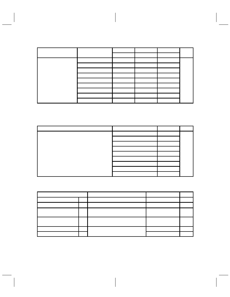
34
3.3.7
Receive Channel Signal-to-Distortion Ratio (see Note 7)
PARAMETER
TEST CONDITIONS
Av = 1
Av = 2
Av = 4
UNIT
PARAMETER
TEST CONDITIONS
MIN
MAX
MIN
MAX
MIN
MAX
UNIT
VI = 6 dB to 0.1 dB
58
§
§
VI = 12 dB to 6 dB
58
58
§
VI = 18 dB to 12 dB
56
58
58
A/D channel signal to
VI = 24 dB to 18 dB
50
56
58
A/D channel signal-to-
distortion ratio
VI = 30 dB to 24 dB
44
50
56
dB
distortion ratio
VI = 36 dB to 30 dB
38
44
50
VI = 42 dB to 36 dB
32
38
44
VI = 48 dB to 42 dB
26
32
38
VI = 54 dB to 48 dB
20
26
32
Av is the programmable gain of the input amplifier.
§ Measurements under these conditions are unreliable due to overrange and signal clipping.
NOTE 7: The test condition is a 1-kHz input signal with a 16-kHz conversion rate. The load impedance for the DAC is
600
. Input and output voltages are referred to Vref.
3.3.8
Transmit Channel Signal-to-Distortion Ratio (see Note 7)
PARAMETER
TEST CONDITIONS
MIN
MAX
UNIT
VI = 6 dB to 0.1 dB
58
VI = 12 dB to 6 dB
58
VI = 18 dB to 12 dB
56
VI = 24 dB to 18 dB
50
D/A channel signal-to-distortion ratio
VI = 30 dB to 24 dB
44
dB
VI = 36 dB to 30 dB
38
VI = 42 dB to 36 dB
32
VI = 48 dB to 42 dB
26
VI = 54 dB to 48 dB
20
NOTE 7: The test condition is a 1-kHz input signal with a 16-kHz conversion rate. The load impedance for the DAC is
600
. Input and output voltages are referred to Vref.
3.3.9
Receive and Transmit Gain and Dynamic Range (see Note 8)
PARAMETER
TEST CONDITIONS
MIN
TYP
MAX
UNIT
Transmit gain tracking error
C, I
VO = 48 dB to 0 dB signal range
±
0.05
±
0.15
dB
Receive gain tracking error
C, I
VI = 48 dB to 0 dB signal range
±
0.05
±
0.15
dB
Transmit gain tracking error
M
VO = 48 dB to 0 dB signal range,
TA = 25
°
C
±
0.05
±
0.25
dB
Receive gain tracking error
M
VI = 48 dB to 0 dB signal range,
TA = 25
°
C
±
0.05
±
0.25
dB
Transmit gain tracking error
M
VO = 48 dB to 0 dB signal range,
±
0.4
dB
Receive gain tracking error
M
O
g
g
TA = 55
°
C TO 125
°
C
±
0.4
dB
NOTE 8: Gain tracking is relative to the absolute gain at 1 kHz and 0 dB (0 dB relative to Vref).
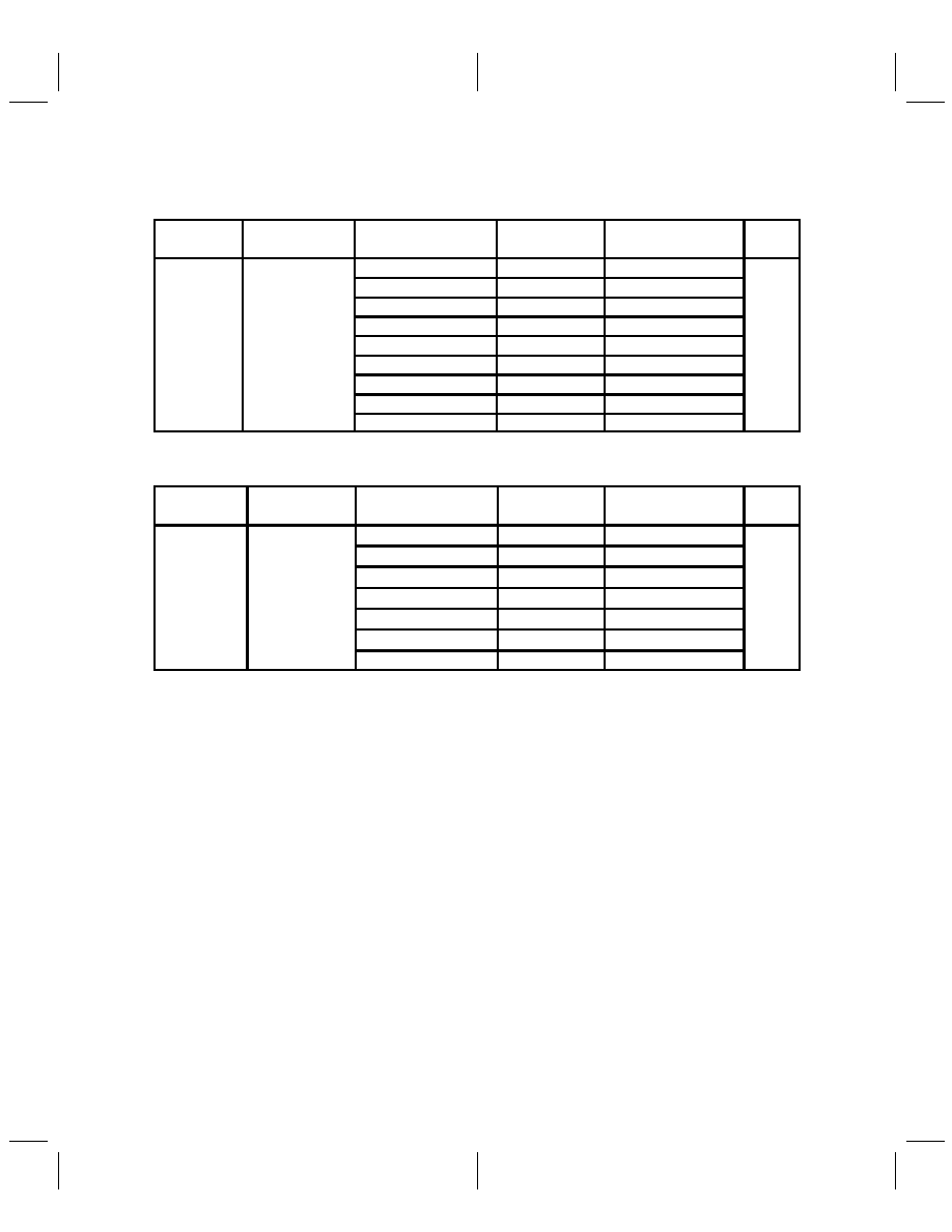
35
3.3.10
Receive Channel Band-Pass Filter Transfer Function, SCF f
clock
= 288 kHz,
Input (IN+ IN ) Is A
±
3-V Sine Wave
(see Note 9)
PARMETER
TEST
FREQUENCY
ADJUSTMENT
MIN
TYP
MAX
UNIT
PARMETER
CONDITION
FREQUENCY
ADJUSTMENT
MIN
TYP
MAX
UNIT
f
100 Hz
K1
×
0 dB
33
29
25
f = 200 Hz
K1
×
0.26 dB
4
2
1
f = 300 Hz to 6200 Hz
K1
×
0 dB
0.25
0
0.25
Input signal
f = 6200 Hz to 6600 Hz
K1
×
0 dB
0.3
0
0.3
Filter gain
Input signal
reference is 0 dB
f = 6600 Hz to 7300 Hz
K1
×
0 dB
0
0.5
dB
reference is 0 dB
f = 7600 Hz
K1
×
2.3 dB
2
0.5
f = 8000 Hz
K1
×
2.7 dB
16
14
f
8800 Hz
K1
×
3.2 dB
40
f
10000 Hz
K1
×
0 dB
65
3.3.11
Receive and Transmit Channel Low-Pass Filter Transfer Function,
SCF f
clock
= 288 kHz (see Note 9)
TEST
FREQUENCY
ADJUSTMENT
MIN
TYP
MAX
UNIT
CONDITION
RANGE
ADDEND
MIN
TYP
MAX
UNIT
f = 0 Hz to 6200 Hz
K1
×
0 dB
0.25
0
0.25
f = 6200 Hz to 6600 Hz
K1
×
0 dB
0.3
0
0.3
I
t i
l
f = 6600 Hz to 7300 Hz
K1
×
0 dB
0.5
0
0.5
Filter gain
Input signal
reference is 0 dB
f = 7600 Hz
K1
×
2.3 dB
2
0.5
dB
reference is 0 dB
f = 8000 Hz
K1
×
2.7 dB
16
14
f
8800 Hz
K1
×
3.2 dB
40
f
10000 Hz
K1
×
0 dB
65
All typical values are at TA = 25
°
C.
The MIN, TYP, and MAX specifications are given for a 288-kHz SCF clock frequency. A slight error in the 288-kHz SCF
may result from inaccuracies in the MSTR CLK frequency, resulting from crystal frequency tolerances. If this frequency
error is less than 0.25%, the ADJUSTMENT ADDEND should be added to the MIN, TYP, and MAX specifications,
where K1 = 100
·
[(SCF frequency 288 kHz)/288 kHz]. For errors greater than 0.25%, see Note 9.
NOTE 9: The filter gain outside of the pass band is measured with respect to the gain at 1 kHz (2 kHz for M version).
The filter gain within the pass band is measured with respect to the average gain within the pass band. The
pass bands are 300 Hz to 7200 Hz and 0 to 7200 Hz for the band-pass and low-pass filters, respectively. For
switched-capacitor filter clocks at frequencies other than 288 kHz, the filter response is shifted by the ratio of
switched-capacitor filter clock frequency to 288 kHz.
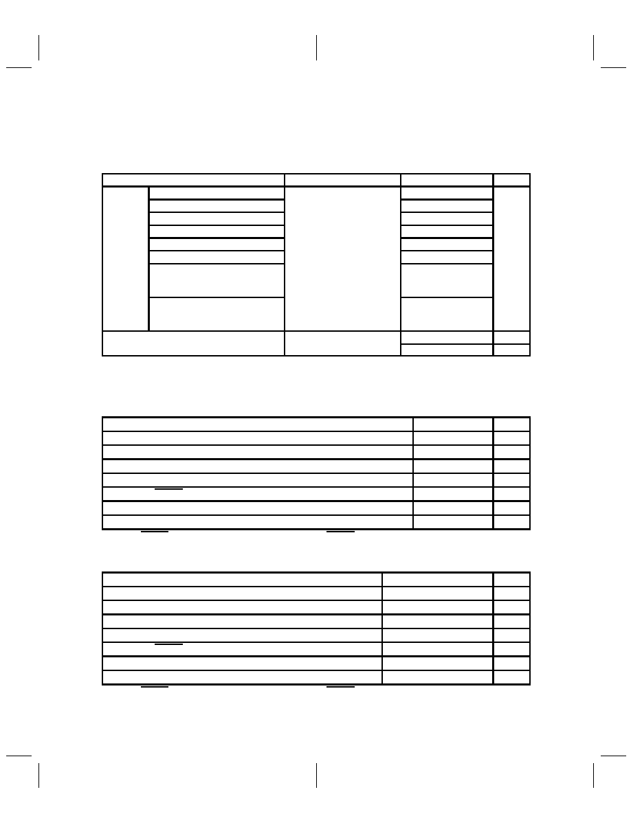
36
3.4
Operating Characteristics Over Recommended Operating Free-Air
Temperature Range, V
CC+
= 5 V, V
CC
= 5 V, V
DD
= 5 V
3.4.1
Receive and Transmit Noise (measurement includes low-pass and band-pass
switched-capacitor filters)
PARAMETER
TEST CONDITIONS
MIN
TYP
MAX
UNIT
Broadband with (sin x)/x
250
500
Broadband without (sin x)/x
200
450
0 to 30 kHz with (sin x)/x
200
400
0 to 30 kHz without (sin x)/x
200
400
T
it
0 to 3.4 kHz with (sin x)/x
DX i
t
00000000000000
180
300
Transmit
noise
0 to 3.4 kHz without (sin x)/x
DX input = 00000000000000,
Constant input code
160
300
µ
Vrms
noise
0 to 6.8 kHz with (sin x)/x
(wide-band operation with 7.2 kHz
roll-off)
Constant in ut code
180
350
µ
0 to 6.8 kHz without (sin x)/x
(wide-band operation with 7.2 kHz
roll-off)
160
350
Receive noise (see Note 10)
Inputs grounded
Gain = 1
300
500
µ
Vrms
Receive noise (see Note 10)
In uts grounded,
Gain = 1
18
dBrnc0
All typical values are at TA = 25
°
C.
NOTE 10: The noise is computed by statistically evaluating the digital output of the A/D converter.
3.5
Timing Requirements
3.5.1
Serial Port Recommended Input Signals, TLC32046C and TLC32046I
PARAMETER
MIN
MAX
UNIT
tc(MCLK)
Master clock cycle time
95
ns
tr(MCLK)
Master clock rise time
10
ns
tf(MCLK)
Master clock fall time
10
ns
Master clock duty cycle
25%
75%
RESET pulse duration (see Note 11)
800
ns
tsu(DX)
DX setup time before SCLK
20
ns
th(DX)
DX hold time after SCLK
tc(SCLK)/4
ns
NOTE 11: RESET pulse duration is the amount of time that the RESET is held below 0.8 V after the power supplies have
reached their recommended values.
3.5.2
Serial Port Recommended Input Signals, TLC32046M
PARAMETER
MIN
TYP
MAX
UNIT
tc(MCLK)
Master clock cycle time
95
ns
tr(MCLK)
Master clock rise time
10
ns
tf(MCLK)
Master clock fall time
10
ns
Master clock duty cycle
50%
RESET pulse duration (see Note 11)
800
ns
tsu(DX)
DX setup time before SCLK
28
ns
th(DX)
DX hold time after SCLK
tc(SCLK)/4
ns
NOTE 11: RESET pulse duration is the amount of time that the RESET is held below 0.8 V after the power supplies have
reached their recommended values.
37
3.5.3
Serial Port AIC Output Signals, C
L
= 30 pF for SHIFT CLK Output, C
L
= 15 pF
For All Other Outputs, TLC32046C and TLC32046I
PARAMETER
MIN
TYP
MAX
UNIT
tc(SCLK)
Shift clock (SCLK) cycle time
380
ns
tf(SCLK)
Shift clock (SCLK) fall time
3
8
ns
tr(SCLK)
Shift clock (SCLK) rise time
3
8
ns
Shift clock (SCLK) duty cycle
45%
55%
td(CH-FL)
Delay from SCLK
to FSR/FSX/FSD
30
ns
td(CH-FH)
Delay from SCLK
to FSR/FSX/FSD
35
90
ns
td(CH-DR)
DR valid after SCLK
90
ns
td(CH-EL)
Delay from SCLK
to EODX/EODR
in word mode
90
ns
td(CH-EH)
Delay from SCLK
to EODX/EODR
in word mode
90
ns
tf(EODX)
EODX fall time
2
8
ns
tf(EODR)
EODR fall time
2
8
ns
td(CH-EL)
Delay from SCLK
to EODX/EODR
in byte mode
90
ns
td(CH-EH)
Delay from SCLK
to EODX/EODR
in byte mode
90
ns
td(MH-SL)
Delay from MSTR CLK
to SCLK
65
170
ns
td(MH-SH)
Delay from MSTR CLK
to SCLK
65
170
ns
Typical values are at TA = 25
°
C.
3.5.4
Serial Port AIC Output Signals, C
L
= 30 pF for SHIFT CLK Output, C
L
= 15 pF
For All Other Outputs, TLC32046M
PARAMETER
MIN
TYP
MAX
UNIT
tc(SCLK)
Shift clock (SCLK) cycle time
400
ns
tf(SCLK)
Shift clock (SCLK) fall time
3
ns
tr(SCLK)
Shift clock (SCLK) rise time
3
ns
Shift clock (SCLK) duty cycle
45%
55%
td(CH-FL)
Delay from SCLK
to FSR/FSX/FSD
30
250
ns
td(CH-FH)
Delay from SCLK
to FSR/FSX/FSD
35
250
ns
td(CH-DR)
DR valid after SCLK
250
ns
td(CH-EL)
Delay from SCLK
to EODX/EODR
in word mode
250
ns
td(CH-EH)
Delay from SCLK
to EODX/EODR
in word mode
250
ns
tf(EODX)
EODX fall time
2
ns
tf(EODR)
EODR fall time
2
ns
td(CH-EL)
Delay from SCLK
to EODX/EODR
in byte mode
250
ns
td(CH-EH)
Delay from SCLK
to EODX/EODR
in byte mode
250
ns
td(MH-SL)
Delay from MSTR CLK
to SCLK
65
170
ns
td(MH-SH)
Delay from MSTR CLK
to SCLK
65
170
ns
Typical values are at TA = 25
°
C.

38
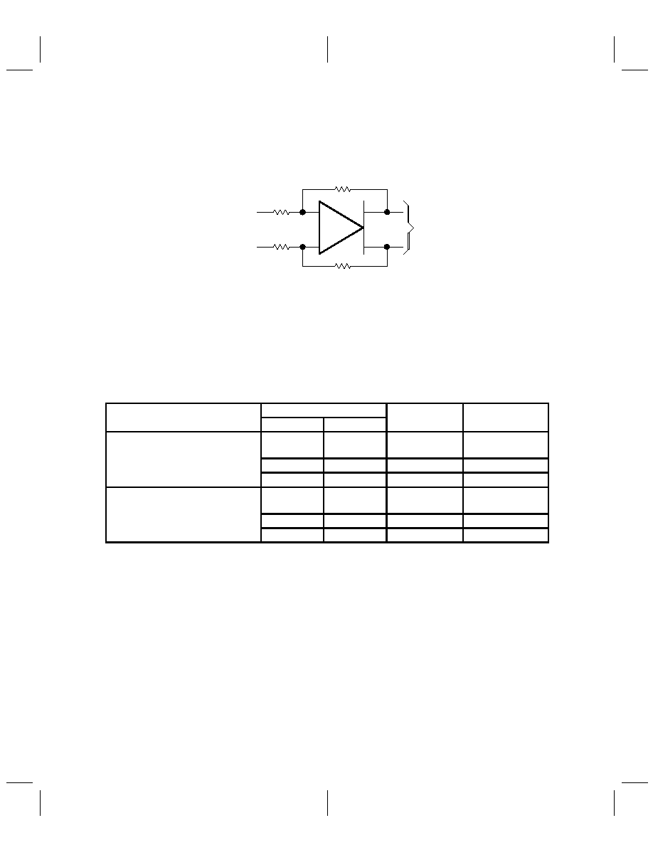
41
4 Parameter Measurement Information
Rfb = 4R for D6 = 0, and D7 = 1
Rfb = 2R for D6 = 1 and D7 = 0
D6 = 0 and D7 = 0
Rfb = R for D6 = 1 and D7 = 1
To Multiplexer
Rfb
+
IN
or
AUX IN
IN +
or
AUX IN +
R
R
+
Rfb
Figure 41. IN + and IN Gain Control Circuitry
Table 41. Gain Control Table (Analog Input Signal Required for
Full-Scale Bipolar A/D Conversion Twos Complement)
INPUT
CONTROL REGISTER BITS
ANALOG
A/D CONVERSION
CONFIGURATIONS
D6
D7
ANALOG
INPUT §
RESULT
1
1
VID =
±
6 V
±
full scale
Differential configuration
A
l
i
t
IN
IN
0
0
VID =
±
6 V
±
full scale
Analog input = IN + IN
= AUX IN + AUX IN
1
0
VID =
±
3 V
±
full scale
= AUX IN + AUX IN
0
1
VID =
±
1.5 V
±
full scale
S
1
1
VI =
±
3 V
±
half scale
Single-ended configuration
Analog input
IN +
ANLG GND
0
0
VI =
±
3 V
±
half scale
Analog input = IN + ANLG GND
= AUX IN + ANLG GND
1
0
VI =
±
3 V
±
full scale
= AUX IN + ANLG GND
0
1
VI =
±
1.5 V
±
full scale
VCC+ = 5 V, VCC = 5 V, VDD = 5 V
VID = Differential Input Voltage, VI = Input voltage referenced to ground with IN or AUX IN connected to GND.
§ In this example, Vref is assumed to be 3 V. In order to minimize distortion, it is recommended that the analog input not
exceed 0.1 dB below full scale.
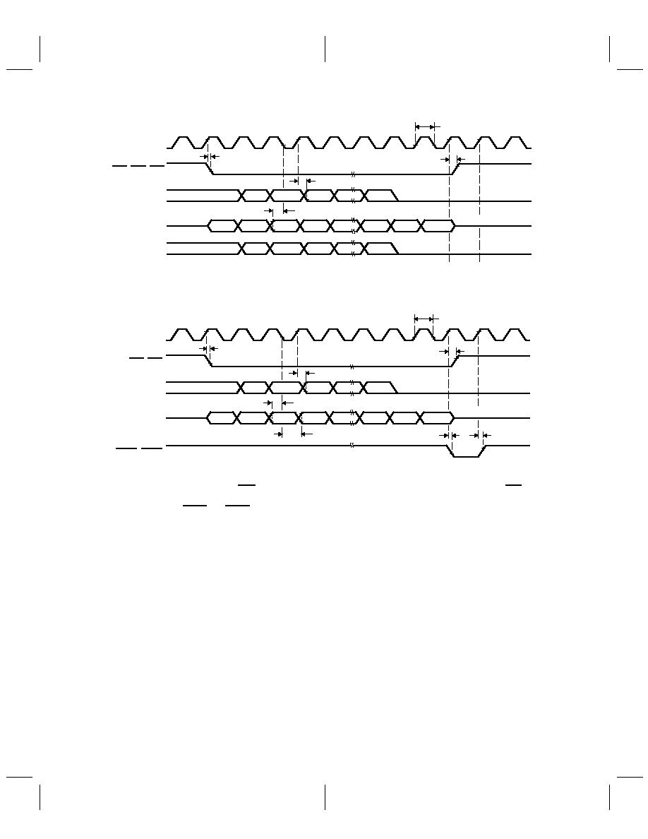
42
DATA-DR
DX
DR
FSX, FSR, FSD
td (CH-DR)
tsu (DX)
D15
D14
D13
D12
D2
D1
D0
Don't Care
D0
D1
D2
D11
D12
D13
D14
D15
D0
D1
D2
D11
D12
D13
D14
D15
8 V
2 V
2 V
8 V
2 V
2 V
8 V
td (CH-FL)
td (CH-FH)
tc (SCLK)
D11
2 V
SHIFT
CLK
Figure 42. Dual-Word (Telephone Interface) Mode Timing
DX
DR
FSX, FSR
td (CHDR)
tsu (DX)
Don't Care
D0
D1
D2
D11
D12
D13
D14
D15
D0
D1
D2
D11
D12
D13
D14
D15
8 V
2 V
2 V
8 V
2 V
2 V
8 V
td (CH-FL)
td (CH-FH)
tc (SCLK)
2 V
SHIFT
CLK
8 V
2 V
th (DX)
td (CH-EL)
td (CH-EH)
EODX, EODR
Figure 43. Word Timing
The time between falling edges of FSR is the A/D conversion period and the time between falling edges of FSX is the
D/A conversion period.
In the word format, EODX and EODR go low to signal the end of a 16-bit data word to the processor. The word-cycle
is 20 shift-clocks wide, giving a four-clock period setup time between data words.
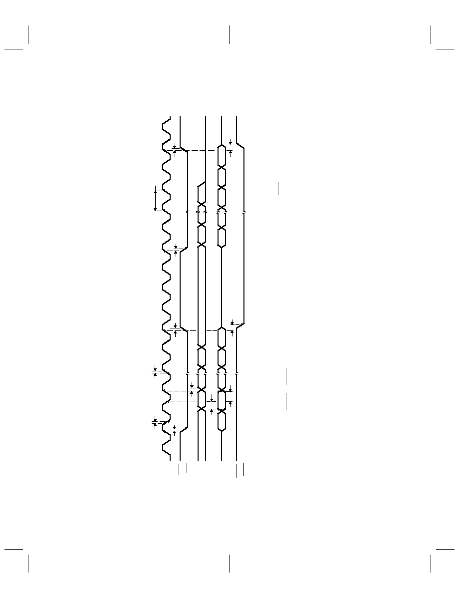
43
SHIFT
CLK
FSR,
FSX
EODR,
EODX
DR
DX
td (CH-FL)
2 V
t f (SCLK)
t r (SCLK)
2 V
td (CH-FH)
2 V
td (CH-FL)
2 V
2 V
td (CH-FH)
tc (SCLK)
2 V
8 V
2 V
2 V
td (CH-DR)
8 V
D15
D14
D13
D9
D8
D7
D6
D2
D1
D0
D12
D11
D8
Don't Care
D13
D9
D15
D14
D0
D2
D1
tsu (DX)
th (DX)
td (CH-EL)
8 V
2 V
The time between falling edges of FSR is the A/D conversion period, and the time between fallling edges of FSX is the D/A conversion period.
In the byte mode, when EODX or EODR is high, the first byte is transmitted or received, and when these signals are low, the second byte is
transmitted or received. Each byte-cycle is 12 shift-clocks long, allowing for a four-shift-clock setup time between byte transmissions.
Figure 44. Byte-Mode Timing
td (CH-EH)
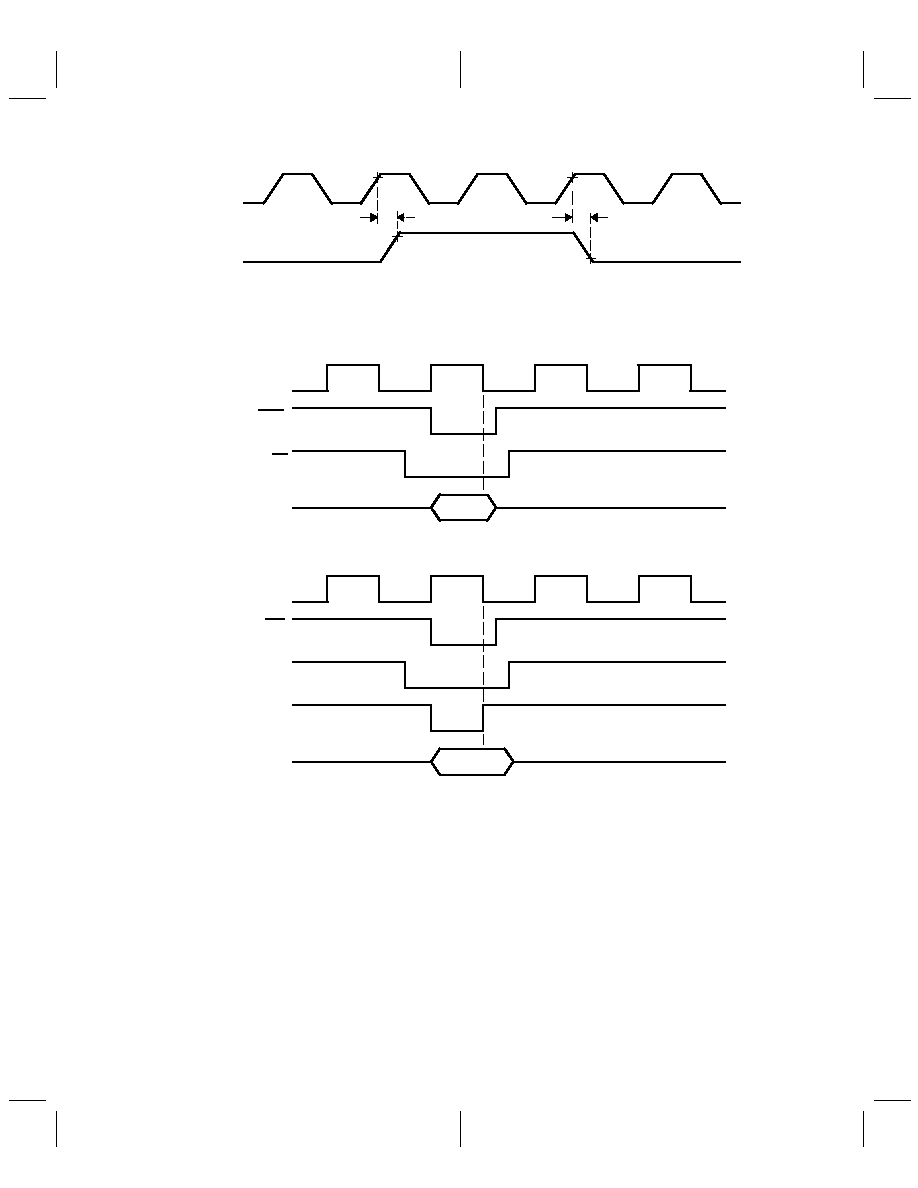
44
SHIFT CLK
MSTR CLK
td (MH-SL)
td (MH-SH)
Figure 4 5. Shift-Clock Timing
4.1
TMS32010/TMS320C15 TLC32046 Interface Circuit
SN74LS299 CLK
SN74LS138 Y1
WE
CLK OUT
D0D15
D0D15
S0,G1
DEN
CLK OUT
Valid
Valid
IN INSTRUCTION TIMING
OUT INSTRUCTION TIMING
Figure 4 6. TMS32010/TMS320C15 TLC32046 Interface Timing
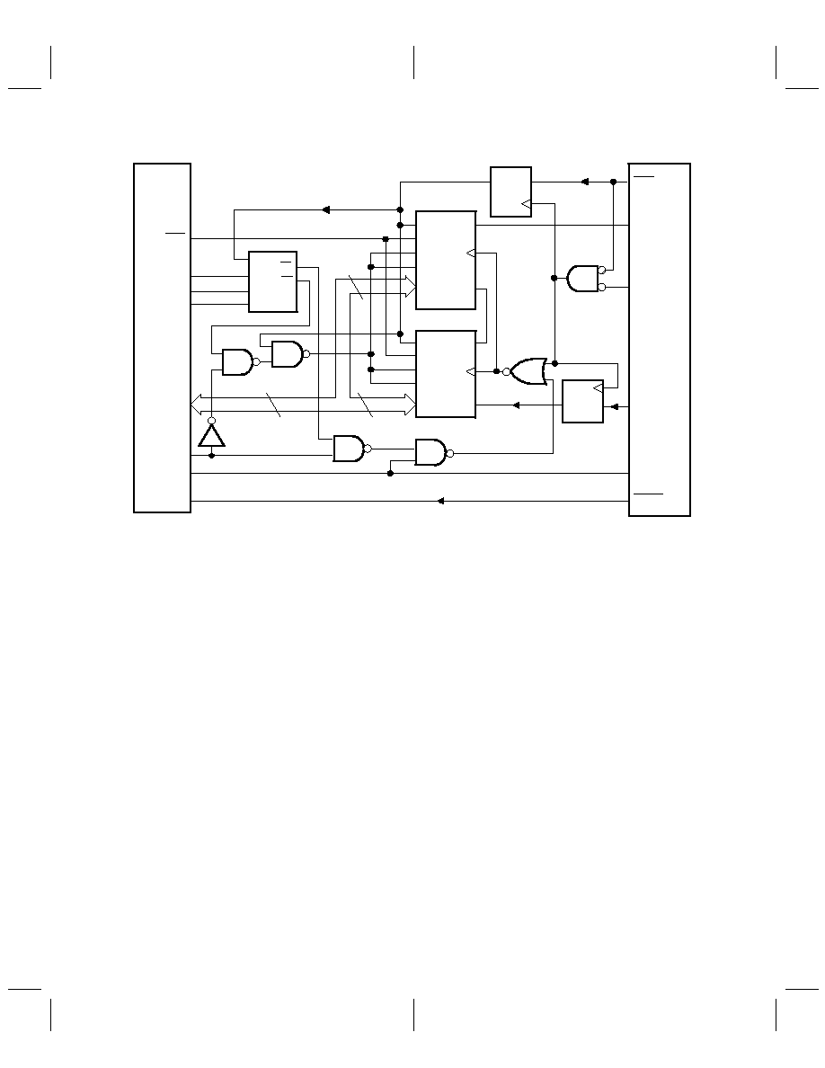
45
DEN
DO D15
WE
CLK
OUT
INT
DO D15
A2/PA2
A1/PA1
A0/PA0
G1
A
B
C
Y1
Y0
SN74LS138
D8 D15
DO D7
SN74LS74
MSTR
CLK
EODX
S1
G2
S0
G1
A H
CLK
SR
Q
H
CLK
SR
AH
G1
S0
G2
S1
SN74LS299
SN74LS299
DR
SHIFT
CLK
DX
FSX
1D
C1
Q
H
Q
SN74LS74
2D
C2
Q
TLC32046
TMS32010
Figure 47. TMS32010/TMS320C15 TLC32046 Interface Circuit

46
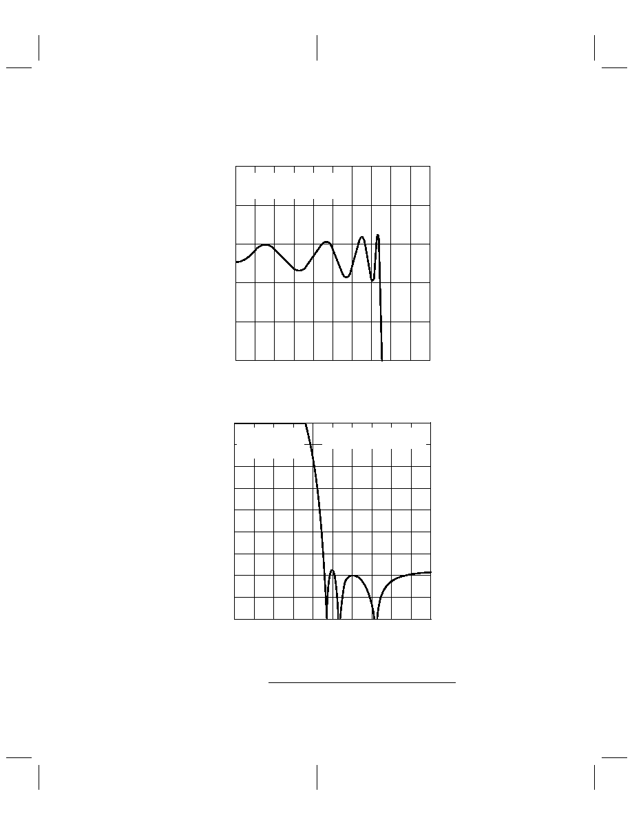
51
5 Typical Characteristics
Normalized Frequency
0.2
0.4
0.6
0
1
2
3
4
5
6
Pass Band Magnitude dB
0
0.2
D/A AND A/D LOW-PASS FILTER
RESPONSE SIMULATION
0.4
7
8
9
10
TA = 25
°
C
Input =
±
3 V Sine Wave
Figure 5 1
50
60
80
90
10
70
0
2
4
6
8
10
12
Magnitude dB
30
40
20
D/A AND A/D LOW-PASS FILTER RESPONSE
0
14
16
18
20
Normalized Frequency
TA = 25
°
C
Input =
±
3 V Sine Wave
See Figure 2-1
for Pass Band
Detail
Figure 5 2
NOTE : Absolute Frequency (kHz)
+
Normalized Frequency
SCF f
clock
(kHz)
288
For Low-Pass SCF f
clock
u
288 kHz, please call the factory.
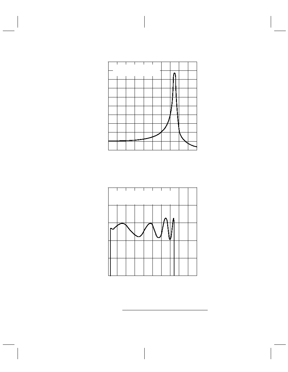
52
0.5
0.4
0.2
0.1
0
0.9
0.3
0
1
2
3
4
5
6
Group Delay ms
0.7
0.6
0.8
D/A AND A/D LOW-PASS GROUP DELAY
7
8
9
10
Normalized Frequency
TA = 25
°
C
Input =
±
3 V Sine Wave
Figure 5 3
Normalized Frequency
0.2
0.4
0.6
0
1
2
3
4
5
6
Pass Band Magnitude dB
0
0.2
A/D BAND-PASS RESPONSE
0.4
7
8
9
10
High-Pass SCF fclock = 16 kHz
TA = 25
°
C
Input =
±
3 V Sine Wave
Figure 5 4
NOTE : Absolute Frequency (kHz)
+
Normalized Frequency
SCF f
clock
(kHz)
288
For Low-Pass SCF f
clock
u
288 kHz, please call the factory.
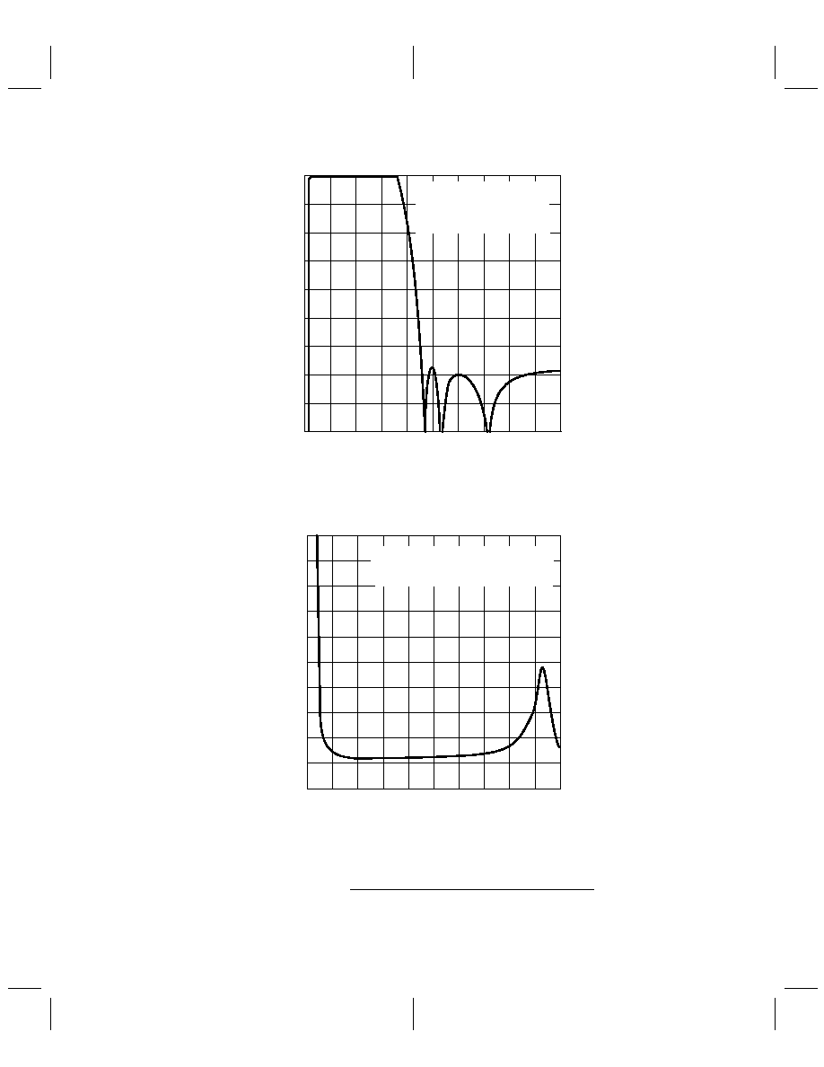
53
50
60
80
100
10
70
0
2
4
6
8
10
12
Magnitude dB
30
40
20
A/D BAND-PASS FILTER RESPONSE SIMULATION
0
14
16
18
20
Normalized Frequency
High-Pass SCF
fclock = 16 kHz
TA = 25
°
C
Input =
±
3 V Sine Wave
Figure 5 5
A/D BAND-PASS FILTER GROUP DELAY
1.1
0.8
0.4
0.2
0
1.8
0.6
0
0.8
1.6
2.4
3.2
4.0
4.8
Group Delay ms
1.4
1.2
1.6
2
5.6
6.4
7.2
8.0
High-Pass SCF fclock = 16 kHz
TA = 25
°
C
Input =
±
3 V Sine Wave
Normalized Frequency
W
Figure 5 6
NOTE : Absolute Frequency (kHz)
+
Normalized Frequency
SCF f
clock
(kHz)
288
For Low-Pass SCF f
clock
u
288 kHz, please call the factory.
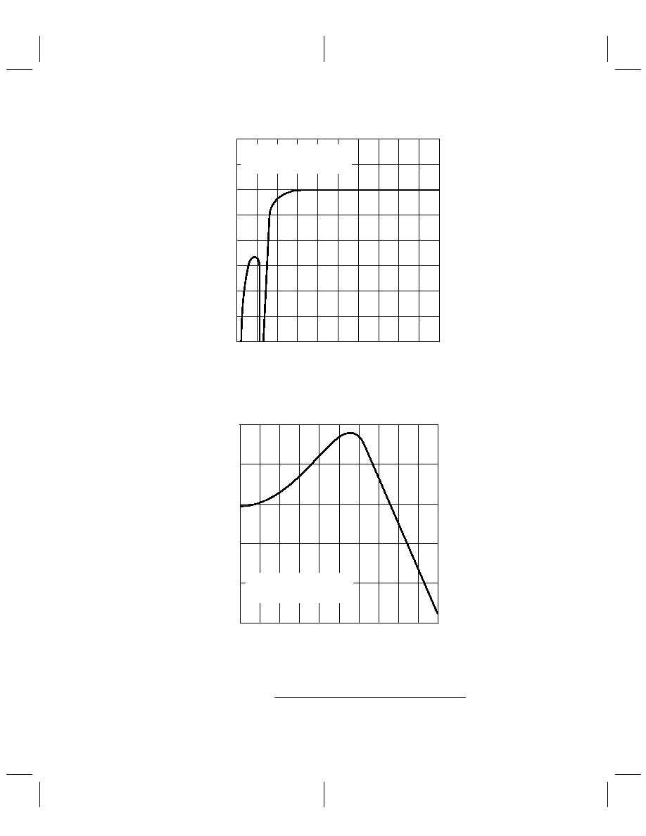
54
20
30
50
60
0
100 200 300 400 500 600
Magnitude dB
10
10
A/D CHANNEL HIGH-PASS FILTER
20
700 800 900 1000
40
0
Normalized Frequency
TA = 25
°
C
Input =
±
3 V Sine Wave
Figure 5 7
D/A (sin x) /x CORRECTION FILTER RESPONSE
Normalized Frequency
2
4
6
0
2
4
6
8
10
12
Magnitude dB
0
2
4
14
16
18
20
TA = 25
°
C
Input =
±
3 V Sine Wave
Figure 5 8
NOTE : Absolute Frequency (kHz)
+
Normalized Frequency
SCF f
clock
(kHz)
288
For Low-Pass SCF f
clock
u
288 kHz, please call the factory.
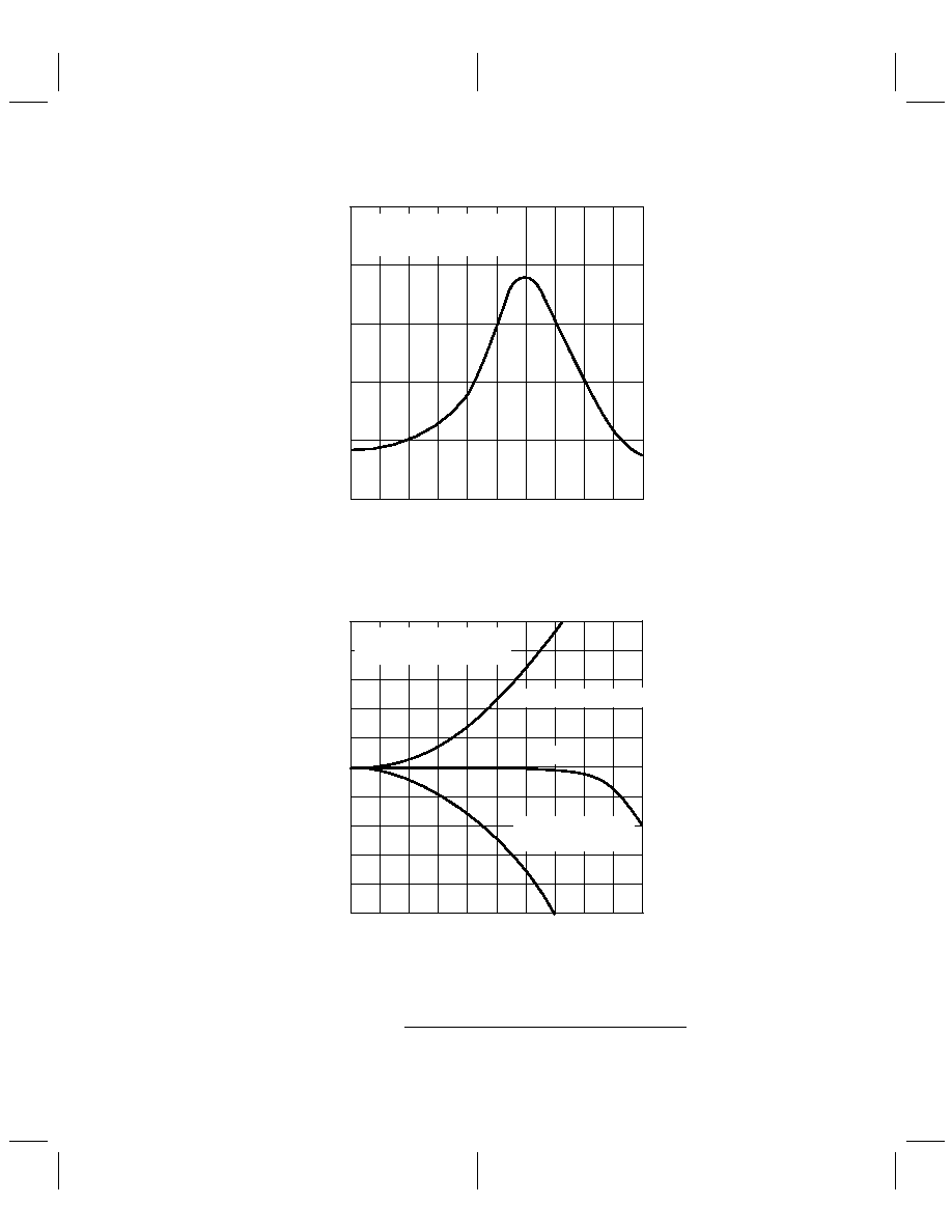
55
D/A (sin x) /x CORRECTION FILTER RESPONSE
Normalized Frequency
200
100
0
0
2
4
6
8
10
12
Group Delay
300
400
500
14
16
18
20
s
µ
TA = 25
°
C
Input =
±
3 V Sine Wave
Figure 5 9
0
0.4
1.2
1.6
2
1.6
0.8
0
1
2
3
4
5
6
Magnitude dB
0.8
0.4
1.2
D/A (sin x) /x CORRECTION ERROR
2
7
8
9
10
(sin x) /x Correction
Error
TA = 25
°
C
Input =
±
3 V Sine Wave
Normalized Frequency
19.2 kHz (sin x) /x
Distortion
Figure 5 10
NOTE : Absolute Frequency (kHz)
+
Normalized Frequency
SCF f
clock
(kHz)
288
For Low-Pass SCF f
clock
u
288 kHz, please call the factory.
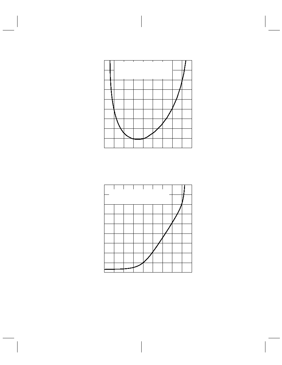
56
f Frequency Hz
A/D BAND-PASS GROUP DELAY
600
560
480
440
520
0.4
0.8
1.2
1.6
2.0
A/D Band-pass Group Delay
680
640
720
2.4
2.8
3.2
3.6
760
µ
s
400
0
Low-pass SCF fclock = 144 kHz
High-pass SCF fclock = 8 kHz
TA = 25
°
C
Input =
±
3 V Sine Wave
Figure 5 11
D/A LOW-PASS GROUP DELAY
360
320
240
200
280
0
0.4
0.8
1.2
1.6
2.0
440
400
520
560
2.4
2.8
3.2
3.6
480
f Frequency Hz
A/D Band-pass Group Delay
µ
s
Low-pass SCF fclock = 144 kHz
TA = 25
°
C
Input =
±
3 V Sine Wave
Figure 5 12
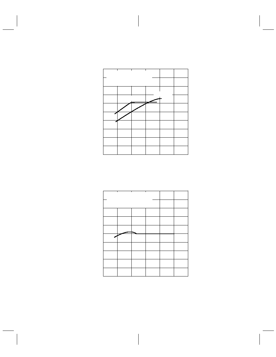
57
A/D SIGNAL-TO-DISTORTION RATIO
vs
INPUT SIGNAL
50
40
20
0
50
40
30
20
10
0
10
Signal-T
o-Distortion Ratio dB
70
80
100
Gain = 4
Gain = 1
1-kHz Input Signal
16-kHz Conversion Rate
TA = 25
°
C
60
30
10
90
Input Signal Relative to Vref dB
Figure 5 13
A/D GAIN TRACKING
(GAIN RELATIVE TO GAIN AT 0-dB INPUT SIGNAL)
0.1
0.3
0.5
50
40
30
20
10
0
10
Gain T
racking dB
0.2
0.3
0.5
1-kHz Input Signal
16-kHz Conversion Rate
TA = 25
°
C
0.1
0.2
0.4
0.4
Input Signal Relative to Vref dB
Figure 5 14
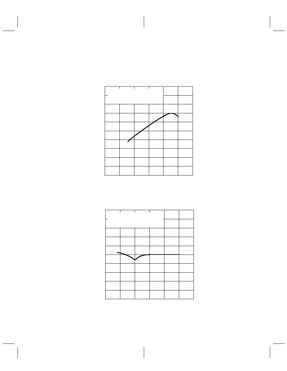
58
D/A CONVERTER SIGNAL-TO-DISTORTION RATIO
vs
INPUT SIGNAL
50
40
20
0
50
40
30
20
10
0
10
Signal-T
o-Distortion Ratio dB
70
80
100
1-kHz Input Signal Into 600
16-kHz Conversion Rate
TA = 25
°
C
60
30
10
90
Input Signal Relative to Vref dB
Figure 5 15
D/A GAIN TRACKING (GAIN RELATIVE TO GAIN
AT 0-dB INPUT SIGNAL)
0
0.1
0.3
0.5
50
40
30
20
10
0
10
Gain T
racking dB
0.2
0.3
0.5
1-kHz Input Signal Into 600
16-kHz Conversion Rate
TA = 25
°
C
0.1
0.2
0.4
0.4
Input Signal Relative to Vref dB
Figure 5 16
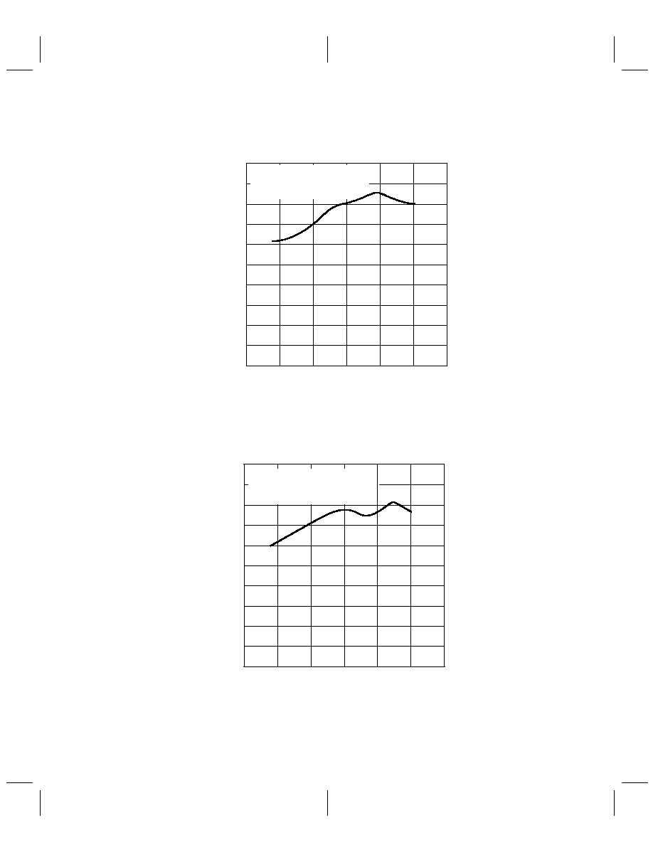
59
A/D SECOND HARMONIC DISTORTION
vs
INPUT SIGNAL
50
40
20
0
50
40
30
20
10
0
10
Second Harmonic Distortion dB
70
80
100
1-kHz Input Signal
16-kHz Conversion Rate
TA = 25
°
C
60
30
10
90
Input Signal Relative to Vref dB
Figure 5 17
D/A SECOND HARMONIC DISTORTION
vs
INPUT SIGNAL
50
40
20
0
50
40
30
20
10
0
10
Second Harmonic Distortion dB
70
80
100
1-kHz Input Signal Into 600
16-kHz Conversion Rate
TA = 25
°
C
60
30
10
90
Input Signal Relative to Vref dB
Figure 5 18
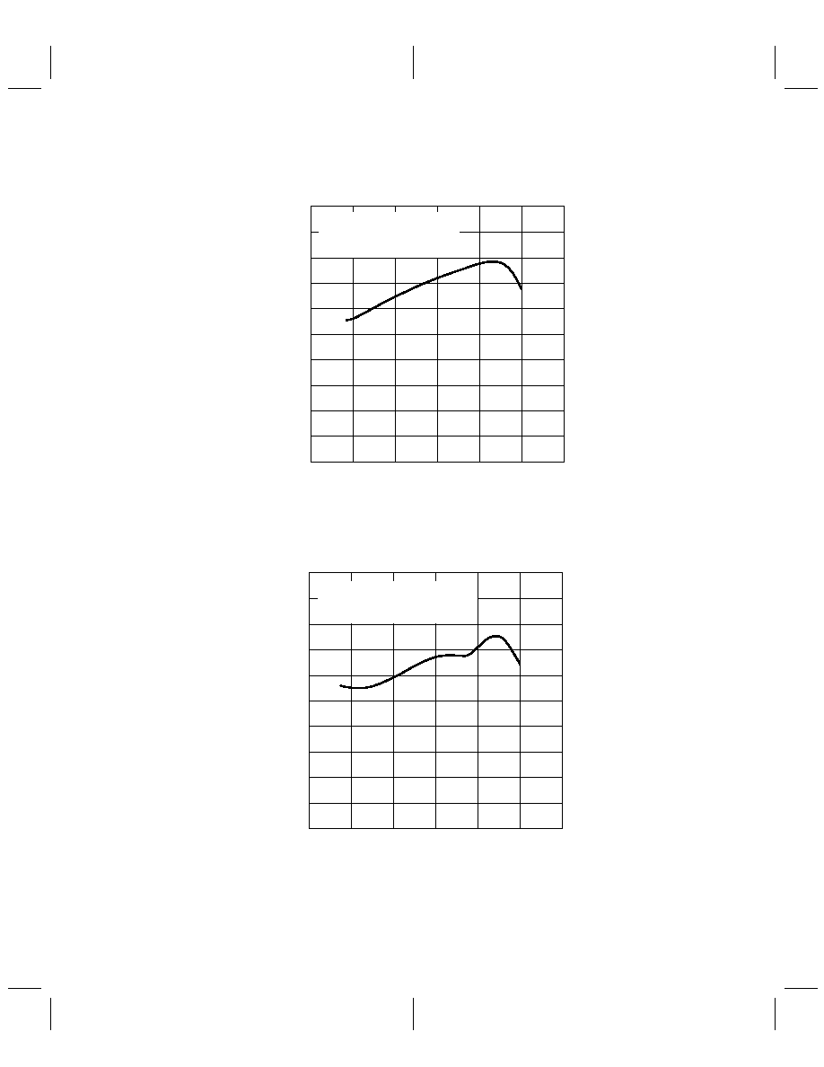
510
A/D THIRD HARMONIC DISTORTION
vs
INPUT SIGNAL
50
40
20
0
50
40
30
20
10
0
10
Third Harmonic Distortion dB
70
80
100
1-Hz Input Signal
16-kHz Conversion Rate
TA = 25
°
C
60
30
10
90
Input Signal Relative to Vref dB
Figure 5 19
D/A THIRD HARMONIC DISTORTION
vs
INPUT SIGNAL
50
40
20
0
50
40
30
20
10
0
10
Third Harmonic Distortion dB
70
80
100
1-kHz Input Signal Into 600
16-kHz Conversion Rate
TA = 25
°
C
60
30
10
90
Input Signal Relative to Vref dB
Figure 5 20
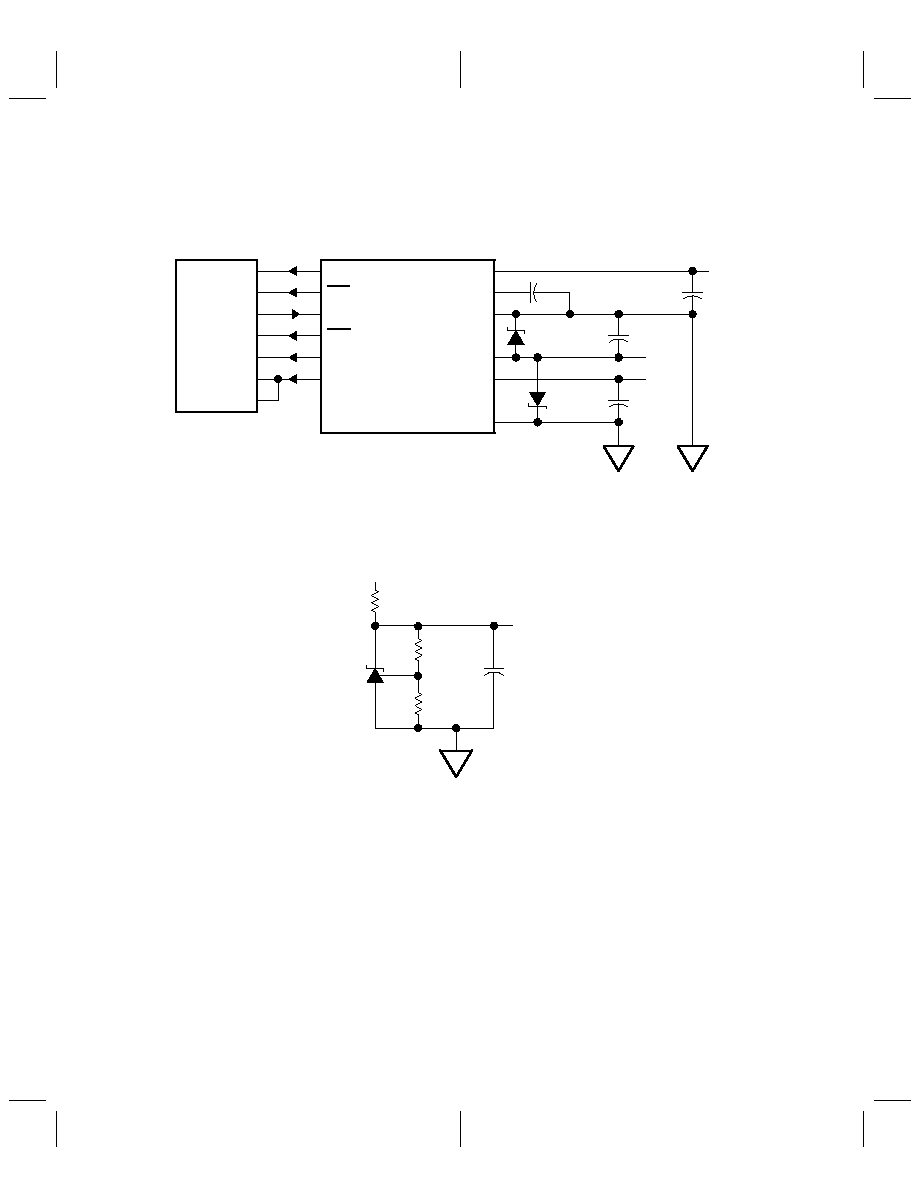
61
6 Application Information
C = 0.2
µ
F, Ceramic
TLC32046
+ 5 V
DGTL GND
VDD
VCC
ANLG GND
REF
VCC +
A
D
C
+ 5 V
5 V
0.1
µ
F
C
C
BAT 42
SHIFT CLK
DR
FSR
DX
FSX
MSTR CLK
TMS32020/C25
CLKX
CLKR
DR
FSR
DX
FSX
CLKOUT
Figure 6 1. AIC Interface to the TMS32020/C25 Showing Decoupling Capacitors
and Schottky Diode
Thomson Semiconductors
VCC = 5 V, R = 1600
VCC = 10 V, R = 5600
FOR: VCC = 12 V, R = 7200
D
3 V Output
0.01
µ
F
TL431
VCC
R
2500
500
Figure 6 2. External Reference Circuit for TLC32046

62

IMPORTANT NOTICE
Texas Instruments and its subsidiaries (TI) reserve the right to make changes to their products or to discontinue
any product or service without notice, and advise customers to obtain the latest version of relevant information
to verify, before placing orders, that information being relied on is current and complete. All products are sold
subject to the terms and conditions of sale supplied at the time of order acknowledgement, including those
pertaining to warranty, patent infringement, and limitation of liability.
TI warrants performance of its semiconductor products to the specifications applicable at the time of sale in
accordance with TI's standard warranty. Testing and other quality control techniques are utilized to the extent
TI deems necessary to support this warranty. Specific testing of all parameters of each device is not necessarily
performed, except those mandated by government requirements.
CERTAIN APPLICATIONS USING SEMICONDUCTOR PRODUCTS MAY INVOLVE POTENTIAL RISKS OF
DEATH, PERSONAL INJURY, OR SEVERE PROPERTY OR ENVIRONMENTAL DAMAGE ("CRITICAL
APPLICATIONS"). TI SEMICONDUCTOR PRODUCTS ARE NOT DESIGNED, AUTHORIZED, OR
WARRANTED TO BE SUITABLE FOR USE IN LIFE-SUPPORT DEVICES OR SYSTEMS OR OTHER
CRITICAL APPLICATIONS. INCLUSION OF TI PRODUCTS IN SUCH APPLICATIONS IS UNDERSTOOD TO
BE FULLY AT THE CUSTOMER'S RISK.
In order to minimize risks associated with the customer's applications, adequate design and operating
safeguards must be provided by the customer to minimize inherent or procedural hazards.
TI assumes no liability for applications assistance or customer product design. TI does not warrant or represent
that any license, either express or implied, is granted under any patent right, copyright, mask work right, or other
intellectual property right of TI covering or relating to any combination, machine, or process in which such
semiconductor products or services might be or are used. TI's publication of information regarding any third
party's products or services does not constitute TI's approval, warranty or endorsement thereof.
Copyright
©
1998, Texas Instruments Incorporated