 | –≠–ª–µ–∫—Ç—Ä–æ–Ω–Ω—ã–π –∫–æ–º–ø–æ–Ω–µ–Ω—Ç: TLC4545 | –°–∫–∞—á–∞—Ç—å:  PDF PDF  ZIP ZIP |
TLC4541, TLC4545
SLAS293 - DECEMBER 2001
5 V, LOW POWER, 16 BIT, 200 KSPS
SERIAL ANALOG TO DIGITAL CONVERTERS WITH AUTO POWER DOWN
1
www.ti.com
FEATURES
D
200-KSPS Sampling Rate
D
Built-In Conversion Clock
D
INL:
±
2.5 LSB Max,
DNL: 2 to -1 LSB Max
D
SINAD = 84.5 dB, SFDR = 95 dB,
THD = 94 dB at 15 kHz f
in
, 200 KSPS
D
SPI/DSP-Compatible Serial Interfaces With
SCLK Input up to 15 MHz
D
Single 5-V Supply
D
Rail-to-Rail Analog Input With 500 kHz BW
D
Two Input Options Available:
- TLC4541 - Single Channel Input
- TLC4545 - Single Channel,
Pseudo-differential Input
D
(TLC4541) Optimized DSP Interface -
Requires FS Input Only
D
Low Power With Auto-Power Down
- Operating Current: 3.5 mA
- Auto-Power Down Current: 5
µ
A
D
Pin Compatible 12/14/16-Bit Family in 8-Pin
SOIC and MSOP Packages
APPLICATIONS
D
ATE System
D
Industrial Process Control
D
Measurement
D
Motor Control
DESCRIPTION
The TLC4541 and TLC4545 are a family of high
performance, 16-bit, low power, miniature CMOS
analog-to-digital converters (ADCs). These devices
operate from a single 5-V supply. Devices are available
with single, dual, or single pseudo-differential inputs. All
of these devices have a chip select (CS), serial clock
(SCLK), and serial data output (SDO) that provides a
direct 3-wire interface to the serial port of most popular
host microprocessors (SPI interface). When interfaced
with a DSP, a frame sync signal (FS) is used to indicate
the start of a serial data frame on either pin 1 (CS) or pin
7 (FS) for the TLC4541. The TLC4545 ADC connects
to the DSP via pin 1 only (CS).
The TLC4541 and TLC4545 are designed to operate
with low power consumption. The power saving feature
is further enhanced with an auto-power down mode.
This product family features a high-speed serial link to
modern host processors with an external SCLK up to
15 MHz. Both families use a built-in oscillator as the
conversion clock, providing a 2.94
µ
s maximum
conversion time.
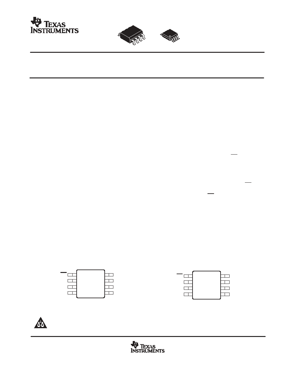
SDO
FS
V
DD
SCLK
8
7
6
5
1
2
3
4
CS
REF
GND
AIN
TLC4541
D OR DGK Package
(TOP VIEW)
SDO
SCLK
V
DD
AIN(-)
8
7
6
5
1
2
3
4
CS
REF
GND
AIN(+)
TLC4545
D OR DGK Package
(TOP VIEW)
PRODUCTION DATA information is current as of publication date.
Products conform to specifications per the terms of Texas Instruments
standard warranty. Production processing does not necessarily include
testing of all parameters.
Copyright
2001, Texas Instruments Incorporated
Please be aware that an important notice concerning availability, standard warranty, and use in critical applications of
Texas Instruments semiconductor products and disclaimers thereto appears at the end of this data sheet.

TLC4541, TLC4545
SLAS293 - DECEMBER 2001
2
www.ti.com
AVAILABLE OPTIONS
TA
PACKAGED DEVICES
TA
8-MSOP (DGK)
8-SOIC (D)
-40
∞
C to 85
∞
C
TLC4541IDGK (PKG Code = ALM)
TLC4541ID
-40
∞
C to 85
∞
C
TLC4545IDGK (PKG Code = AME)
TLC4545ID
functional block diagram
SDO
REF
GND
CONTROL
LOGIC
LOW POWER
SAR ADC
SCLK
FS
OSC
TLC4541
S/H
AIN
REF
GND
CONTROL
LOGIC
LOW POWER
SAR ADC
Conversion
Clock
SCLK
OSC
TLC4545
S/H
SDO
AIN (+)
AIN (-)
VDD
VDD
Conversion
Clock
CS
CS
TLC4541, TLC4545
SLAS293 - DECEMBER 2001
3
www.ti.com
Terminal Functions
TLC4541 single channel unipolar ADCs
TERMINAL
I/O
DESCRIPTION
NAME
NO.
I/O
DESCRIPTION
AIN
4
I
Analog input channel
CS
1
I
Chip select. A high-to-low transition on the CS input removes SDO from a high-impedance state within a
maximum delay time. If the TLC4541 is attached to a dedicated TMS320 DSP serial port using the FS input,
CS can be grounded.
FS
7
I
DSP frame sync input. Indication of a start of a serial data frame. A low-to-high transition removes SDO from
the high-impedance state and the MSB is presented. Tie this pin to VDD if not used.
GND
3
I
Ground return for the internal circuitry. Unless otherwise noted, all voltage measurements are with respect to
GND.
SDO
8
O
The 3-state serial data output for the A/D conversion result. SDO is kept in the high-impedance state when
CS is high. The output format is MSB first. Remaining data bits are presented on the rirsing edge of SCLK.
When FS is not active (FS = 1 at the falling edge of CS): The MSB is presented on the SDO pin on the falling
edge of CS after a maximum delay time. Data is valid on each falling edge of SCLK until all data is read.
When FS is active (FS = 0 at the falling edge of CS): The MSB is presented to the SDO output on the rising
edge of FS. Data is valid on the falling edge SCLK and changes on the rising edge SCLK (this is typically
used with an active FS from a DSP).
SDO returns to the high-impedance state after the 17th rising edge on SCLK. If a 17th SCLK cycle is not
presented, as is the case when using an SPI host, SDO returns to the high-impedance state on the rising
edge of CS.
SCLK
5
I
Serial clock. This terminal receives the serial SCLK from the host processor.
REF
2
I
External voltage reference input
VDD
6
I
Positive supply voltage
TLC4545 single channel pseudo-differential ADCs
TERMINAL
I/O
DESCRIPTION
NAME
NO.
I/O
DESCRIPTION
AIN0 (+)
4
I
Positive analog input for the TLC4545.
AIN1 (-)
5
I
Inverted analog input for the TLC4545.
CS
1
I
Chip select. A high-to-low transition on CS removes SDO from the high-impedance state within a maximum
delay time. The CS input can be connected to a DSP frame sync (FS) output when a dedicated TMS320 DSP
serial port is used.
GND
3
I
Ground return for the internal circuitry. Unless otherwise noted, all voltage measurements are with respect to
GND.
SDO
8
O
The 3-state serial data output for the A/D conversion result. SDO is kept in the high-impedance state when
CS is high and presents output data after the CS falling edge until the LSB is presented. The output format is
MSB first. The remaining data bits are presented on the rising edge of SCLK. Output data is valid on each
falling edge of SCLK until all data is read. SDO returns to the high-impedance state after the 17th rising edge
on SCLK. If a 17th SCLK cycle is not presented, as is the case when using an SPI host, SDO returns to the
high-impedance state on the rising edge of CS.
SCLK
7
I
Serial clock. This terminal receives the serial SCLK from the host processor.
REF
2
I
External voltage reference input
VDD
6
I
Positive supply voltage
TLC4541, TLC4545
SLAS293 - DECEMBER 2001
4
www.ti.com
absolute maximum ratings over operating free-air temperature (unless otherwise noted)
Supply voltage, GND to V
DD
-0.3 V to 6.5V
. . . . . . . . . . . . . . . . . . . . . . . . . . . . . . . . . . . . . . . . . . . . . . . . . . . . . . . .
Analog input voltage range
-0.3 V to V
DD
+0.3 V
. . . . . . . . . . . . . . . . . . . . . . . . . . . . . . . . . . . . . . . . . . . . . . . . . . . .
Reference input voltage
V
DD
+0.3 V
. . . . . . . . . . . . . . . . . . . . . . . . . . . . . . . . . . . . . . . . . . . . . . . . . . . . . . . . . . . . . . .
Digital input voltage range
-0.3 V to V
DD
+0.3 V
. . . . . . . . . . . . . . . . . . . . . . . . . . . . . . . . . . . . . . . . . . . . . . . . . . . . .
Operating virtual junction temperature range, T
J
-40
∞
C to 150
∞
C
. . . . . . . . . . . . . . . . . . . . . . . . . . . . . . . . . . . . . .
Operating free-air temperature range: T
A
(I)
-40
∞
C to 85
∞
C
. . . . . . . . . . . . . . . . . . . . . . . . . . . . . . . . . . . . . . . . . .
Storage temperature range, T
stg
-65
∞
C to 150
∞
C
. . . . . . . . . . . . . . . . . . . . . . . . . . . . . . . . . . . . . . . . . . . . . . . . . . .
Lead temperature 1,6 mm (1/16 inch) from case for 10 seconds
260
∞
C
. . . . . . . . . . . . . . . . . . . . . . . . . . . . . . . .
Stresses beyond those listed under "absolute maximum ratings" may cause permanent damage to the device. These are stress ratings only, and
functional operation of the device at these or any other conditions beyond those indicated under "recommended operating conditions" is not
implied. Exposure to absolute-maximum-rated conditions for extended periods may affect device reliability.
recommended operating conditions
MIN
NOM
MAX
UNIT
Supply voltage, VDD
4.5
5
5.5
V
Frequency, SCLK
VDD = 2.7 V to 5.5 V
100
15000
kHz
Tolerable clock jitter, SCLK
VDD = 2.7 V to 5.5 V
24
ps
Aperature jitter
VDD = 2.7 V to 5.5 V
100
ps
External reference voltage input, VREF
4
VDD
V
VREF input impedance
VDD = 5 V, CS = 1, SCLK = 0
100
M
VREF input impedance
VDD = 5 V, CS = 0, SCLK = 15 MHz
20
25
k
External reference input current
VDD = VREF = 4.5 V, CS=0, SCLK = 15 MHz
0.02
1
mA
Analog input voltage
AIN, AIN(+)
0
VDD
V
Analog input voltage
AIN(-)
-0.2
0.2
V
High level control input voltage, VIH
2.1
V
Low level control input voltage, VIL
0.8
V
Operating free-air temperature, TA
TLC4541/45I
-40
85
∞
C
TLC4541, TLC4545
SLAS293 - DECEMBER 2001
5
www.ti.com
electrical characteristics over recommended operating free-air temperature range,
V
DD
= 5 V, V
REF
= 4.096 V, SCLK frequency = 15 MHz (unless otherwise noted)
PARAMETER
TEST CONDITIONS
MIN
TYP
MAX
UNIT
VOH
High-level output voltage
VDD = 4.5 V,
IOH = -0.2 mA
3.9
V
VOL
Low-level output voltage
VDD = 4.5 V,
IOL = 0.8 mA
0.4
V
IOZ
Off-state output current
VO = VDD, CS = VDD
1
2.5
A
IOZ
Off-state output current
(high-impedance-state)
VO = 0,
CS = VDD
-1
-2.5
µ
A
IIH
High-level input current
VI = VDD
0.005
2.5
µ
A
IIL
Low-level input current
VI = 0
-0.005
2.5
µ
A
ICC
Operating supply current
CS at 0 V,
VDD = 4.5 V to 5.5 V
3.5
mA
ICC(PD) Power-down supply current
For all digital inputs, 0
VI
0.3 V or
VI
VDD - 0.3 V, SCLK=VDD,
VDD = 4.5 V to 5.5 V
3
5
µ
A
Selected analog input channel
Selected channel at VDD
1
A
Selected analog input channel
leakage current
Selected channel at 0 V
-1
µ
A
Ci
Input capacitance
Analog inputs
11
14
pF
Ci
Input capacitance
Control Inputs
20
25
pF
Zi
Input resistance
VDD = 5.5 V
500
ac specifications (TLC4541/45)
PARAMETER
TEST CONDITIONS
MIN
TYP
MAX
UNIT
SINAD
Signal-to-noise ratio + distortion
fI = 15 kHz at 200 KSPS
84.5
dB
SNR
Signal-to-noise ratio
fI = 15 kHz at 200 KSPS
85
dB
THD
Total harmonic distortion
TLC4541
fI = 15 kHz at 200 KSPS
-94
-87
dB
THD
Total harmonic distortion
TLC4545
fI = 15 kHz at 200 KSPS
-94
-89
dB
ENOB
Effective number of bits
fI = 15 kHz at 200 KSPS
13.7
Bits
SFDR
Spurious free dynamic range
TLC4541
fI = 15 kHz at 200 KSPS
-95
-87
dB
SFDR
Spurious free dynamic range
TLC4545
fI = 15 kHz at 200 KSPS
-95
-89
dB
Full power bandwidth, -3 dB, analog input
1
MHz
Full power bandwidth, -1 dB, analog input
500
kHz
Crosstalk
0.25 LBS
80
dB
dc specifications (TLC4541/45)
PARAMETER
TEST CONDITIONS
MIN
TYP
MAX
UNIT
INL
Integral linearity error (see Note 1)
-2.5
2.5
LSB
DNL
Differential linearity error
-1
2
LSB
EO
Offset error (see Note 2)
TLC4541
-3.5
3.5
mV
EO
Offset error (see Note 2)
TLC4545
-1
1
mV
EG
Gain error (see Note 2)
TLC4541
-2
2
mV
EG
Gain error (see Note 2)
TLC4545
-1.8
1.8
mV
All typical values are at VDD = 5 V, TA = 25
∞
C.
NOTES:
1. Linear error is the maximum deviation from the best straight line through the A/D transfer characteristics.
2. Zero error is the difference between 0000h and the converted output for zero input voltage: full-scale error is the difference between
ideal full-scale and the converted output for full-scale input voltage.