TLE214x, TLE214xA, TLE214xY
EXCALIBUR LOW-NOISE HIGH-SPEED
PRECISION OPERATIONAL AMPLIFIERS
SLOS183A ≠ FEBRUARY 1997 ≠ REVISED MARCH 1998
1
POST OFFICE BOX 655303
∑
DALLAS, TEXAS 75265
D
Low Noise
10 Hz . . . 15 nV/
Hz
1 kHz . . . 10.5 nV/
Hz
D
10 000-pF Load Capability
D
20-mA Min Short-Circuit Output Current
D
27-V/
µ
s Min Slew Rate
D
High Gain-Bandwidth Product . . . 5.9 MHz
D
Low V
IO
. . . 500
µ
V Max at 25
∞
C
D
Single or Split Supply . . . 4 V to 44 V
D
Fast Settling Time
340 ns to 0.1%
400 ns to 0.01%
D
Saturation Recovery . . . 150 ns
D
Large Output Swing
V
CC ≠
+ 0.1 V to V
CC +
≠ 1 V
description
The TLE214x and TLE214xA devices are high-performance, internally compensated operational amplifiers
built using Texas Instruments complementary bipolar Excalibur process. The TLE214xA is a tighter offset
voltage grade of the TLE214x. Both are pin-compatible upgrades to standard industry products.
The design incorporates an input stage that simultaneously achieves low audio-band noise of 10.5 nV/
Hz with
a 10-Hz 1/f corner and symmetrical 40-V/
µ
s slew rate typically with loads up to 800 pF. The resulting low
distortion and high power bandwidth are important in high-fidelity audio applications. A fast settling time of
340 ns to 0.1% of a 10-V step with a 2-k
/100-pF load is useful in fast actuator/positioning drivers. Under similar
test conditions, settling time to 0.01% is 400 ns.
The devices are stable with capacitive loads up to 10 nF, although the 6-MHz bandwidth decreases to 1.8 MHz
at this high loading level. As such, the TLE214x and TLE214xA are useful for low-droop sample-and-holds and
direct buffering of long cables, including 4-mA to 20-mA current loops.
The special design also exhibits an improved insensitivity to inherent integrated circuit component mismatches
as is evidenced by a 500-
µ
V maximum offset voltage and 1.7-
µ
V/
∞
C typical drift. Minimum common-mode
rejection ratio and supply-voltage rejection ratio are 85 dB and 90 dB, respectively.
Device performance is relatively independent of supply voltage over the
±
2-V to
±
22-V range. Inputs can
operate between V
CC ≠
≠ 0.3 to V
CC +
≠ 1.8 V without inducing phase reversal, although excessive input current
may flow out of each input exceeding the lower common-mode input range. The all-npn output stage provides
a nearly rail-to-rail output swing of V
CC ≠
≠ 0.1 to V
CC +
≠ 1 V under light current-loading conditions. The device
can sustain shorts to either supply since output current is internally limited, but care must be taken to ensure
that maximum package power dissipation is not exceeded.
Both versions can also be used as comparators. Differential inputs of V
CC
±
can be maintained without damage
to the device. Open-loop propagation delay with TTL supply levels is typically 200 ns. This gives a good
indication as to output stage saturation recovery when the device is driven beyond the limits of recommended
output swing.
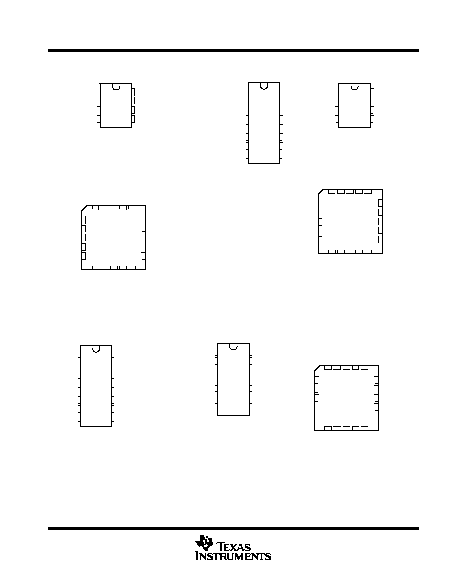
Both the TLE214x and TLE214xA are available in a wide variety of packages, including both the
industry-standard 8-pin small-outline version and chip form for high-density system applications. The C-suffix
devices are characterized for operation from 0
∞
C to 70
∞
C, I-suffix devices from ≠ 40
∞
C to 105
∞
C, and M-suffix
devices over the full military temperature range of ≠ 55
∞
C to 125
∞
C.
Copyright
©
1998, Texas Instruments Incorporated
PRODUCTION DATA information is current as of publication date.
Products conform to specifications per the terms of Texas Instruments
standard warranty. Production processing does not necessarily include
testing of all parameters.
Please be aware that an important notice concerning availability, standard warranty, and use in critical applications of
Texas Instruments semiconductor products and disclaimers thereto appears at the end of this data sheet.
TLE214x, TLE214xA, TLE214xY
EXCALIBUR LOW-NOISE HIGH-SPEED
PRECISION OPERATIONAL AMPLIFIERS
SLOS183A ≠ FEBRUARY 1997 ≠ REVISED MARCH 1998
2
POST OFFICE BOX 655303
∑
DALLAS, TEXAS 75265
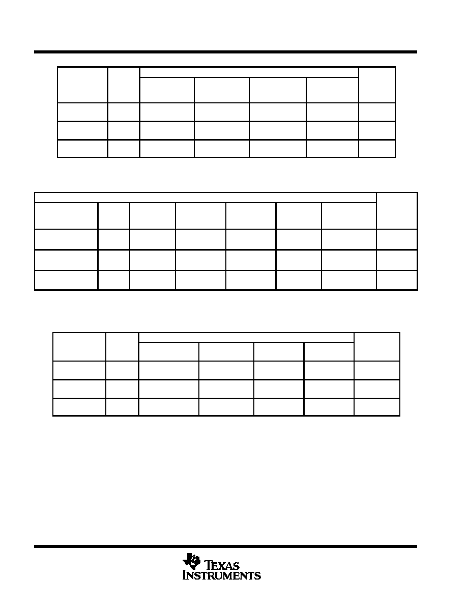
TLE2141 AVAILABLE OPTIONS
PACKAGED DEVICES
CHIP
TA
VIOmax
AT 25
∞
C
SMALL OUT-
LINE
(D)
CHIP CARRIER
(FK)
CERAMIC DIP
(JG)
PLASTIC DIP
(P)
CHIP
FORM
(Y)
0
∞
C to 70
∞
C
500
µ
V
900
µ
V
TLE2141ACD
TLE2141CD
--
--
TLE2141ACP
TLE2141CP
--
≠ 40
∞
C to 105
∞
C
500
µ
V
900
µ
V
TLE2141AID
TLE2141ID
--
--
TLE2141AIP
TLE2141IP
TLE2141Y
≠ 55
∞
C to 125
∞
C
500
µ
V
900
µ
V
TLE2141AMD
TLE2141MD
TLE2141AMFK
TLE2141MFK
TLE2141AMJG
TLE2141MJG
TLE2141AMP
TLE2141MP
--
The D packages are available taped and reeled. Add R suffix to device type (e.g., TLE2141ACDR).
Chip forms are tested at TA = 25
∞
C only.
TLE2142 AVAILABLE OPTIONS
PACKAGED DEVICES
CHIP
TA
VIOmax
AT 25
∞
C
SMALL
OUTLINE
(D)
CHIP
CARRIER
(FK)
CERAMIC
DIP
(JG)
PLASTIC
DIP
(P)
TSSOP
(PW)
CHIP
FORMß
(Y)
0
∞
C to 70
∞
C
750
µ
V
TLE2142ACD
--
--
TLE2142ACP
--
0
∞
C to 70
∞
C
1200
µ
V
TLE2142CD
--
--
TLE2142CP
TLE2142CPWLE
--
40
∞
C to 105
∞
C
750
µ
V
TLE2142AID
--
--
TLC2142AIP
--
TLE2142Y
≠ 40
∞
C to 105
∞
C
1200
µ
V
TLE2142ID
--
--
TLC2142IP
--
TLE2142Y
55
∞
C to 125
∞
C
750
µ
V
TLE2142AMD
TLE2142AMFK
TLE2142AMJG
TLC2142AMP
--
≠ 55
∞
C to 125
∞
C
1200
µ
V
TLE2142MD
TLE2142MFK
TLE2142MJG
TLC2142MP
--
--
The D packages are available taped and reeled. Add R suffix to device type (e.g., TLC2142ACDR).
The PW packages are available left-ended taped and reeled. Add LE the suffix to device type (e.g., TLC2142CPWLE).
ß Chip forms are tested at TA = 25
∞
C only.
TLE2144 AVAILABLE OPTIONS
VIOmax
PACKAGED DEVICES
CHIP FORM
TA
VIOmax
AT 25
∞
C
SMALL OUTLINE
(DW)
CHIP CARRIER
(FK)
CERAMIC DIP
(J)
PLASTIC DIP
(N)
CHIP FORM
(Y)
0
∞
C to 70
∞
C
1.5 mV
2.4 mV
--
TLE2144CDW
--
--
--
--
TLE2144ACN
TLE2144CN
--
≠ 40
∞
C to 105
∞
C
1.5 mV
2.4 mV
--
TLE2144IDW
--
--
--
--
TLE2144AIN
TLE2144IN
TLE2144Y
≠ 55
∞
C to 125
∞
C
1.5 mV
2.5 mV
--
TLE2144MDW
TLE2144AMFK
TLE2144MFK
TLE2144AMJ
TLE2144MJ
TLE2144AMN
TLE2144MN
--
The DW packages are available taped and reeled. Add R suffix to device type (e.g., TLE2144CDWR).
Chip forms are tested at TA = 25
∞
C only.
TLE214x, TLE214xA, TLE214xY
EXCALIBUR LOW-NOISE HIGH-SPEED
PRECISION OPERATIONAL AMPLIFIERS
SLOS183A ≠ FEBRUARY 1997 ≠ REVISED MARCH 1998
4
POST OFFICE BOX 655303
∑
DALLAS, TEXAS 75265
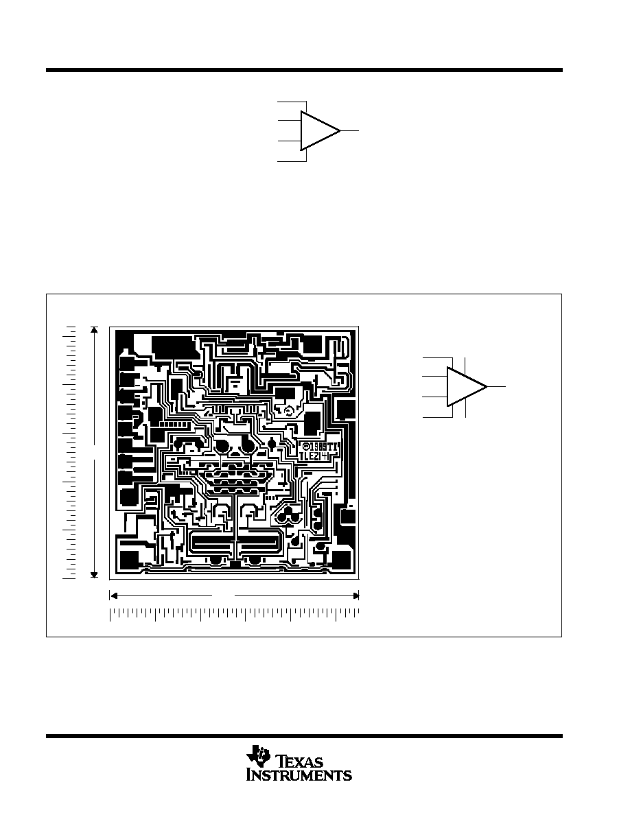
symbol
+
≠
OUT
IN +
IN ≠
OFFSET N1
(see Note A)
OFFSET N2
(see Note A)
NOTES: A. OFFSET N1 AND OFFSET N2
are only availiable on the
TLE2241x devices.
TLE2141Y chip information
This chip, when properly assembled, displays characteristics similar to the TLE2141. Thermal compression or
ultrasonic bonding may be used on the doped-aluminum bonding pads. Chips may be mounted with conductive
epoxy or a gold-silicon preform.
BONDING PAD ASSIGNMENTS
CHIP THICKNESS: 15 TYPICAL
BONDING PADS: 4
◊
4 MINIMUM
TJmax = 150
∞
C
TOLERANCES ARE
±
10%.
ALL DIMENSIONS ARE IN MILS.
+
≠
OUT
IN +
IN ≠
VCC+
(7)
(3)
(2)
(6)
(4)
VCC ≠
(1)
(5)
OFFSET N1
OFFSET N2
65
64
(7)
(6)
(5)
(4)
(3)
(2)
(1)
TLE214x, TLE214xA, TLE214xY
EXCALIBUR LOW-NOISE HIGH-SPEED
PRECISION OPERATIONAL AMPLIFIERS
SLOS183A ≠ FEBRUARY 1997 ≠ REVISED MARCH 1998
5
POST OFFICE BOX 655303
∑
DALLAS, TEXAS 75265
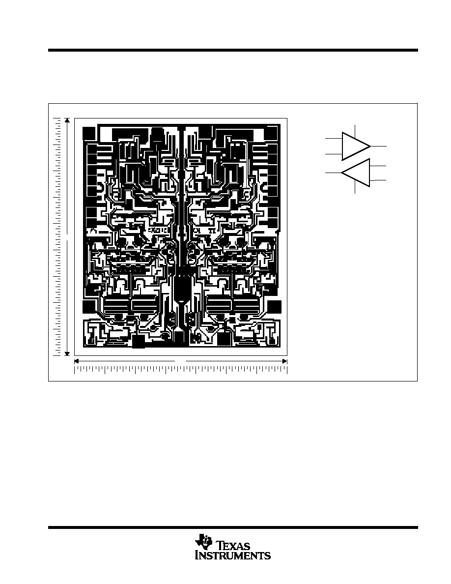
TLE2142Y chip information
This chip, when properly assembled, displays characteristics similar to the TLE2142. Thermal compression or
ultrasonic bonding may be used on the doped-aluminum bonding pads. Chips may be mounted with conductive
epoxy or a gold-silicon preform.
BONDING PAD ASSIGNMENTS
CHIP THICKNESS: 15 TYPICAL
BONDING PADS: 4
◊
4 MINIMUM
TJmax = 150
∞
C
TOLERANCES ARE
±
10%.
ALL DIMENSIONS ARE IN MILS.
PIN 4 IS INTERNALLY CONNECTED
TO BACKSIDE OF CHIP.
+
≠
1OUT
1IN +
1IN ≠
VCC+
(8)
(6)
(3)
(2)
(5)
(1)
≠
+
(7)
2IN +
2IN ≠
2OUT
(4)
VCC ≠
90
80
(1)
(2)
(3)
(4)
(5)
(6)
(7)
(8)