
TLK2500IRCP
1.6 Gbps to 2.5 Gbps TRANSCEIVER
SLLS356B ≠ JUNE 1999 ≠ REVISED JANUARY 2000
1
POST OFFICE BOX 655303
∑
DALLAS, TEXAS 75265
D
1.6 to 2.5 Gigabits Per Second (Gbps)
Serializer/Deserializer
D
Hot Plug Protection
D
High-Performance 64-Pin VQFP Thermally
Enhanced Package (PowerPAD
TM
)
D
2.5-V Power Supply for Low-Power
Operation
D
Programmable Voltage Output Swing on
Serial Output
D
Interfaces to Back Plane, Copper Cables or
Optical Converters
D
On-Chip 8B/10B Encoding/Decoding,
Comma and Synch
D
On-Chip PLL Provides Clock Synthesis
From Low-Speed Reference
D
Receiver Differential Input Thresholds
200 mV Min
D
Typical Power 350 mW
D
16-Bit Parallel LV TTL (3.3 V) Compatible
Data Interface
D
Transmitter Pre-Emphasis/De-Emphasis for
Improved Signal Integraity
D
Rated for Industrial Temperature Range
D
Ideal for High-Speed Back Plane
Interconnect and Point-to-Point Data Links
description
The TLK2500 multigigabit transceiver can be used for ultra-high-speed bidirectional point-to-point data
transmissions. The TLK2500 supports an effective serial interface speed of 1.6 Gbps to 2.5 Gbps.
The primary application of this chip is to provide very high-speed I/O data channels for point-to-point baseband
data transmission over controlled impedance media of approximately 50
. The transmission media can be
printed-circuit board, copper cables, or fiber-optic cable. The maximum rate and distance of data transfer is
dependent upon the attenuation characteristics of the media and the noise coupling to the environment.
This device can also be used to replace parallel data transmission architectures by providing a reduction in the
number of traces, connector pins, and transmit/receive pins. Parallel data loaded into the transmitter is delivered
to the receiver over a serial channel, which can be a coaxial copper cable, a controlled impedance back plane,
or an optical link. It is then reconstructed into its original parallel format. It offers significant power and cost
savings over current solutions as well as scalability for higher and lower data rates in the future.
The TLK2500 performs the data parallel-to-serial, serial-to-parallel conversion, and clock extraction functions
for a physical layer interface device. The serial transceiver interface operates at a maximum speed of 2.5 Gbps.
The transmitter latches 16-bit parallel data at a rate based on the supplied reference clock. The 16-bit parallel
data is internally encoded into 20 bits using an 8B/10B encoding format. The resulting 20-bit word is then
transmitted differentially at 20x the reference clock rate. The receiver section performs the serial-to-parallel
conversion on the input data synchronizing the resulting 20-bit wide parallel data to the extracted reference
clock. It then decodes the 20-bit wide data using 8B/10B decoding format resulting in 16 bits of parallel data
at the receive data pins. This results in an effective data payload of 1.28 Gbps to 2 Gbps (16-bit data
◊
clock
rate).
The TLK2500 is housed in a high-performance, thermally enhanced, 64-pin VQFP PowerPAD package. Use
of the PowerPAD package does not require any special considerations except to note that the PowerPAD, which
is an exposed die pad on the bottom of the device, is a metallic thermal and electrical conductor. It is
recommended that the TLK2500 PowerPAD
be soldered to the thermal land on the board. All ac performance
specifications in this datasheet are measured with the PowerPAD soldered to the test board.
The TLK2500 uses a 2.5 V supply. The I/O section is 3.3-V compatible. With the 2.5 V supply, the chipset is very
power efficient dissipating less than 350 mW typically.
The TLK2500 is designed to be hot-plug capable. A power-on reset holds the receiver clock low and puts the
parallel-side output signal pins into a high-impedance state during power up as well as serial outputs.
Copyright
©
2000, Texas Instruments Incorporated
PRODUCTION DATA information is current as of publication date.
Products conform to specifications per the terms of Texas Instruments
standard warranty. Production processing does not necessarily include
testing of all parameters.
Please be aware that an important notice concerning availability, standard warranty, and use in critical applications of
Texas Instruments semiconductor products and disclaimers thereto appears at the end of this data sheet.
PowerPAD is a trademark of Texas Instruments Incorporated.

TLK2500IRCP
1.6 Gbps to 2.5 Gbps TRANSCEIVER
SLLS356B ≠ JUNE 1999 ≠ REVISED JANUARY 2000
3
POST OFFICE BOX 655303
∑
DALLAS, TEXAS 75265
transmit interface
The transmitter portion registers incoming 16-bit wide data (TXD[0:15]) on the rising edge of GTX_CLK. The
data is then 8B/10B encoded, serialized and transmitted sequentially over the differential high speed I/O
channel. The clock multiplier, multiplies the reference clock (GTX_CLK) by a factor of 10 times, providing a
signal which is fed to the parallel-to-serial shift register. Data is transmitted LSB (D0) first. The transmitter also
outputs commas when the link is idle for byte synchronization. The transmitter depends on the receive side
being active to achieve link synchronization. This provides automatic sync and resync during normal operation,
as needed. The LCKREFN pin can be used to override this feature.
low-speed data bus
The transmit bus interface accepts 16 bit wide single-ended TTL parallel data at the TXD[0≠15] pins. Data is
valid on the rising edge of GTX_CLK when TX_EN is asserted high. The GTX_CLK is used as the byte clock.
The data, enable and clock signals must be properly aligned as shown in Figure 1. Detailed timing information
can be found in the TTL input switching characteristics table.
GTX_CLK
TX_EN, TX_ER
TXDn
tSETUP
tHOLD
Figure 1. Transmit Timing Waveform
transmission latency
The data transmission latency of the TLK2500 is defined as the delay from the initial 16-bit word load to the serial
transmission of bit 0. The minimum latency is 34 bit times; the maximum is 38 bit times.
Tx Word A
Tx Word B
T latency
DOUTTXP,
DOUTTXN
TXD[0≠15]
GTX_CLK
Tx Word C
Tx Word B
This figure for illustration only. Tlatency is larger than shown.
Figure 2. Transmitter Latency
TLK2500IRCP
1.6 Gbps to 2.5 Gbps TRANSCEIVER
SLLS356B ≠ JUNE 1999 ≠ REVISED JANUARY 2000
4
POST OFFICE BOX 655303
∑
DALLAS, TEXAS 75265
transmit interface (continued)
8b/10b encoder
All true serial interfaces require a method of encoding to insure minimum transition density so that the receiving
PLL has a minimal number of transitions in which to stay locked on. The encoding scheme maintains the signal
dc balance by keeping the number of ones and zeros the same. This provides good transition density for clock
recovery and improves error checking. The TLK2500 uses the 8B/10B encoding algorithm that is used by Fibre
channel and gigabit ethernet. This is transparent to the user as the TLK2500 devices internally encode and
decode the data such that the user reads and writes actual 16≠bit data.
The 8B/10B encoder converts 8 bit wide data to a 10 bit wide encoded data character to improve its transmission
characteristics. Since the TLK2500 is a 16 bit wide interface the data is split into two 8 bit wide bytes for
encoding. Each byte is fed into a separate encoder. The encoding is dependant upon two additional input
signals, TX_EN and TX_ER. When TX_EN is asserted and TX_ER is deasserted then the data bits TXD[0≠15]
are encoded and transmitted normally. When TX_EN is deasserted and TX_ER is asserted, then the encoder
will generate a carrier extend consisting of two K23.7 codes. If TX_EN and TX_ER are both asserted then the
encoder will generate an error event. This error event consists of one or more code-groups that are not part of
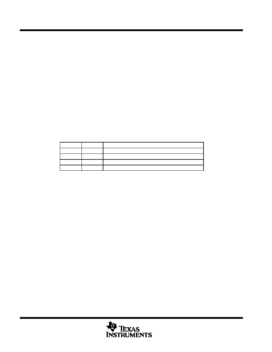
the valid data or delimiter set somewhere in the frame being transmitted. Table 1 provides the transmit data
control decoding.
Table 1. Transmit Data Controls
TX_EN
TX_ER
ENCODED 10 BIT OUTPUT
0
0
IDLE (<K28.5, D5.6>,<K28.5, D16.2>)
0
1
Carrier extend (K23.7)
1
0
Normal data character
1
1
Transmit error propagation (invalid code group)
IDLE generation
The encoder sends the IDLE character set when no payload data is available to be sent and TX_EN/TX_ER
are deasserted. IDLE consists of a K28.5 code and either a D5.6 or D16.2 character. Since data is latched into
the TLK2500 16 bits at a time, this in turn is converted into two 10 bit codes that are transmitted sequentially.
This means IDLE consists of two 10 bit codes, being 20 bits wide that is transmitted during a single GTX_CLK
cycle. IDLE will replace data during initial synchronization or resync, until synchronization is achieved (see
synchronization and initialization).
PRBS generator
The TLK2500 has a pseudo random bit stream (PRBS) function. When the PRBSEN pin is forced high, the
PRBS test is enabled. A PRBS is generated and fed into the 10 bit parallel-to-serial converter input register. Data
from the normal input source is ignored during the PRBS mode. The PRBS pattern is then fed through the
transmit circuitry as if it were normal data and sent out to the transmitter. The output can be sent to a bit error
rate tester (BERT) or to the receiver of another TLK2500. Since the PRBS is not really random but a
predetermined sequence of ones and zeroes the data can be captured and checked for errors by a BERT.
Results are reported on the RX_ER/PRBSPASS pin.
parallel to serial
The parallel-to-serial shift register takes in 10 bit wide data multiplexed from the two 8B/10B encoders and
converts it to a serial stream. The shift register is clocked by the internally generated bit clock, which is 10
◊
the
GTX_CLK input frequency. The LSB (D0) is transmitted first.

TLK2500IRCP
1.6 Gbps to 2.5 Gbps TRANSCEIVER
SLLS356B ≠ JUNE 1999 ≠ REVISED JANUARY 2000
5
POST OFFICE BOX 655303
∑
DALLAS, TEXAS 75265
transmit interface (continued)
high-speed data output
The high speed data output driver consists of a differential pair (CML) that can be optimized for a particular
transmission line impedance and length. The line can be directly coupled or ac coupled. The drivers provide
pre-emphasis and de-emphasis. Pre-emphasis is a boost in the serial driver current occurring during a bit
transition (either high-to-low or low-to-high). This current is held for one bit time. De-emphasis is a reduction
in the serial driver current directly following a pre-emphasis event if there is not a transition after the
pre-emphasis event. De-emphasis can be held for multiple bit times if no transition occurs. Refer to Figure 10
and Figure 11 for termination details.
receive interface
The receiver portion of the TLK2500 accepts 8B/10B encoded differential serial data. The interpolator and clock
recovery circuit will lock to the data stream and extract the bit rate clock. This recovered clock is used to retime
the input data stream. The serial data is then aligned to two separate 10-bit word boundaries, 8B/10B decoded
and output on a 16 bit wide parallel bus synchronized to the extracted receive clock.
low-speed data bus
The receive bus interface drives 16 bit wide single-ended TTL parallel data at the RXD[0≠15] pins. Data is valid
on the rising edge of RX_CLK when RX_DV is asserted high. The RX_CLK is used as the byte clock. The data,
enable and clock signals must be properly aligned as shown in Figure 3. Detailed timing information can be
found in the TTL output switching characteristics table.
RX_CLK
RXDn, RX_ER, RX_DV
tSETUP
tHOLD
Figure 3. Receive Timing Waveform
data reception latency
The serial-to-parallel data latency is the time from when the first bit arrives at the receiver until it is output in the
aligned parallel word with RXD0 received as first bit. The minimum latency is 76 bit times; the maximum is 107
bit times.
