Document Outline
- features
- description
- functional block diagram
- ORDERING INFORMATION
- Terminal Functions
- detailed description
- serial interface
- I/O CLK
- microprocessor serial interface
- DSP interface
- input data bits
- analog inputs and internal test voltages
- converter
- extended sampling, asynchronous start of sampling: CSTART\ operation
- reference voltage inputs
- programmable conversion rate
- programmable power-down state
- power up and initialization
- input clock inversion Ö INV CLK\
- absolute maximum ratings over operating free-air temperature range (unless otherwise noted)Å
- recommended operating conditions
- electrical characteristics over recommended operating free-air temperature range, VCC = Vref+ = 2.7 V to 5.5 V, I/ O CLK frequency = 2.2 MHz ( unless otherwise noted)
- operating characteristics over recommended operating free-air temperature range, VCC = Vref+ = 2.7 V to 5.5 V, I/ O CLK frequency = 2.2 MHz ( unless otherwise noted)
- PARAMETER MEASUREMENT INFORMATION
- TYPICAL CHARACTERISTICS
- APPLICATION INFORMATION
- simplified analog input analysis
- maximum conversion throughput
TLV1548-EP
LOW-VOLTAGE 10-BIT ANALOG-TO-DIGITAL CONVERTER
WITH SERIAL CONTROL AND 8 ANALOG INPUTS
SGLS171 ≠ JUNE 2003
1
POST OFFICE BOX 655303
∑
DALLAS, TEXAS 75265
D
Controlled Baseline
≠ One Assembly Site, One Test Site, One
Fabrication Site
D
Extended Temperature Performance of
≠40
∞
C to 125
∞
C
D
Enhanced Diminishing Manufacturing
Sources (DMS) Support
D
Enhanced Product-Change Notification
D
Qualification Pedigree
D
Conversion Time
10
µ
s
D
10-Bit-Resolution ADC
D
Programmable Power-Down
Mode . . . 1
µ
A
D
Wide Range Single-Supply Operation of
2.7 V dc to 5.5 V dc
D
Analog Input Range of 0 V to V
CC
D
Built-in Analog Multiplexer with 8 Analog
Input Channels
Component qualification in accordance with JEDEC and industry
standards to ensure reliable operation over an extended
temperature range. This includes, but is not limited to, Highly
Accelerated Stress Test (HAST) or biased 85/85, temperature
cycle, autoclave or unbiased HAST, electromigration, bond
intermetallic life, and mold compound life. Such qualification
testing should not be viewed as justifying use of this component
beyond specified performance and environmental limits.
D
TMS320 DSP and Microprocessor SPI and
QSPI Compatible Serial Interfaces
D
End-of-Conversion (EOC) Flag
D
Inherent Sample-and-Hold Function
D
Built-In Self-Test Modes
D
Programmable Power and Conversion Rate
D
Asynchronous Start of Conversion for
Extended Sampling
D
Hardware I/O Clock Phase Adjust Input
description
The TLV1548 is a CMOS 10-bit switched-capacitor successive-approximation (SAR) analog-to-digital (A/D)
converter. The device has a chip select (CS), input-output clock (I/O CLK), data input (DATA IN) and serial data
output (DATA OUT) that provides a direct 4-wire synchronous serial peripheral interface (SPI
, QSPI
) port
of a host microprocessor. When interfacing with a TMS320 DSP, an additional frame sync signal (FS) indicates
the start of a serial data frame. The device allows high-speed data transfers from the host. The INV CLK input
provides further timing flexibility for the serial interface.
In addition to a high-speed converter and versatile control capability, the device has an on-chip 11-channel
multiplexer that can select any one of eight analog inputs or any one of three internal self-test voltages. The
sample-and-hold function is automatic except for the extended sampling cycle, where the sampling cycle is
started by the falling edge of asynchronous CSTART. At the end of the A/D conversion, the end-of-conversion
(EOC) output goes high to indicate that the conversion is complete. The TLV1548 is designed to operate with
a wide range of supply voltages with very low power consumption. The power saving feature is further enhanced
with a software-programmed power-down mode and conversion rate. The converter incorporated in the device
features differential high-impedance reference inputs that facilitate ratiometric conversion, scaling, and
isolation of analog circuitry from logic and supply noise. A switched-capacitor design allows low-error
conversion over the full operating temperature range.
The TLV1548 has eight analog input channels. The TLV1548Q is characterized for operation from ≠40
∞
C to
125
∞
C.
Copyright
2003, Texas Instruments Incorporated
PRODUCTION DATA information is current as of publication date.
Products conform to specifications per the terms of Texas Instruments
standard warranty. Production processing does not necessarily include
testing of all parameters.
Please be aware that an important notice concerning availability, standard warranty, and use in critical applications of
Texas Instruments semiconductor products and disclaimers thereto appears at the end of this data sheet.
SPI and QSPI are registered trademarks of Motorola, Inc.
1
2
3
4
5
6
7
8
9
10
20
19
18
17
16
15
14
13
12
11
A0
A1
A2
A3
A4
A5
A6
A7
CSTART
GND
V
CC
EOC
I/O CLK
DATA IN
DATA OUT
CS
REF+
REF≠
FS
INV CLK
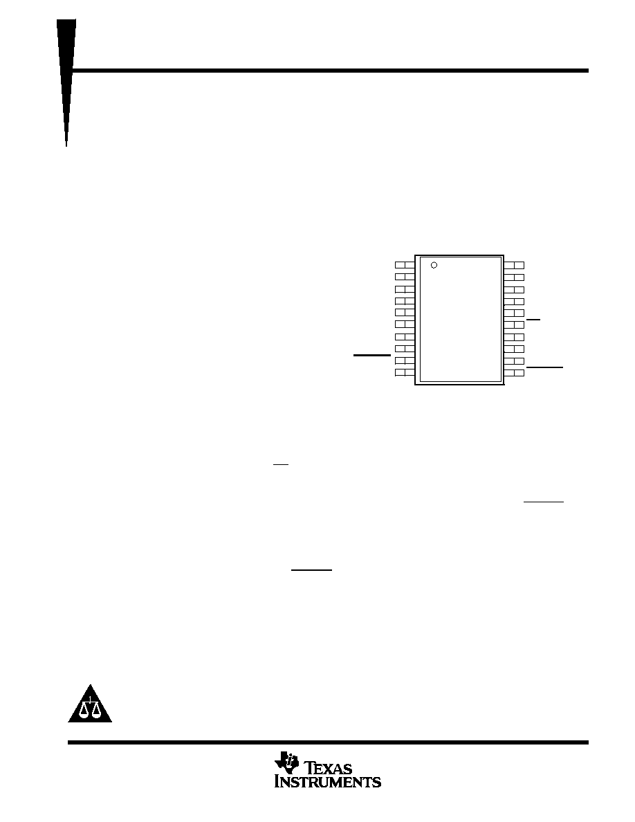
DB PACKAGE
(TOP VIEW)
TLV1548-EP
LOW-VOLTAGE 10-BIT ANALOG-TO-DIGITAL CONVERTER
WITH SERIAL CONTROL AND 8 ANALOG INPUTS
SGLS171 ≠ JUNE 2003
2
POST OFFICE BOX 655303
∑
DALLAS, TEXAS 75265
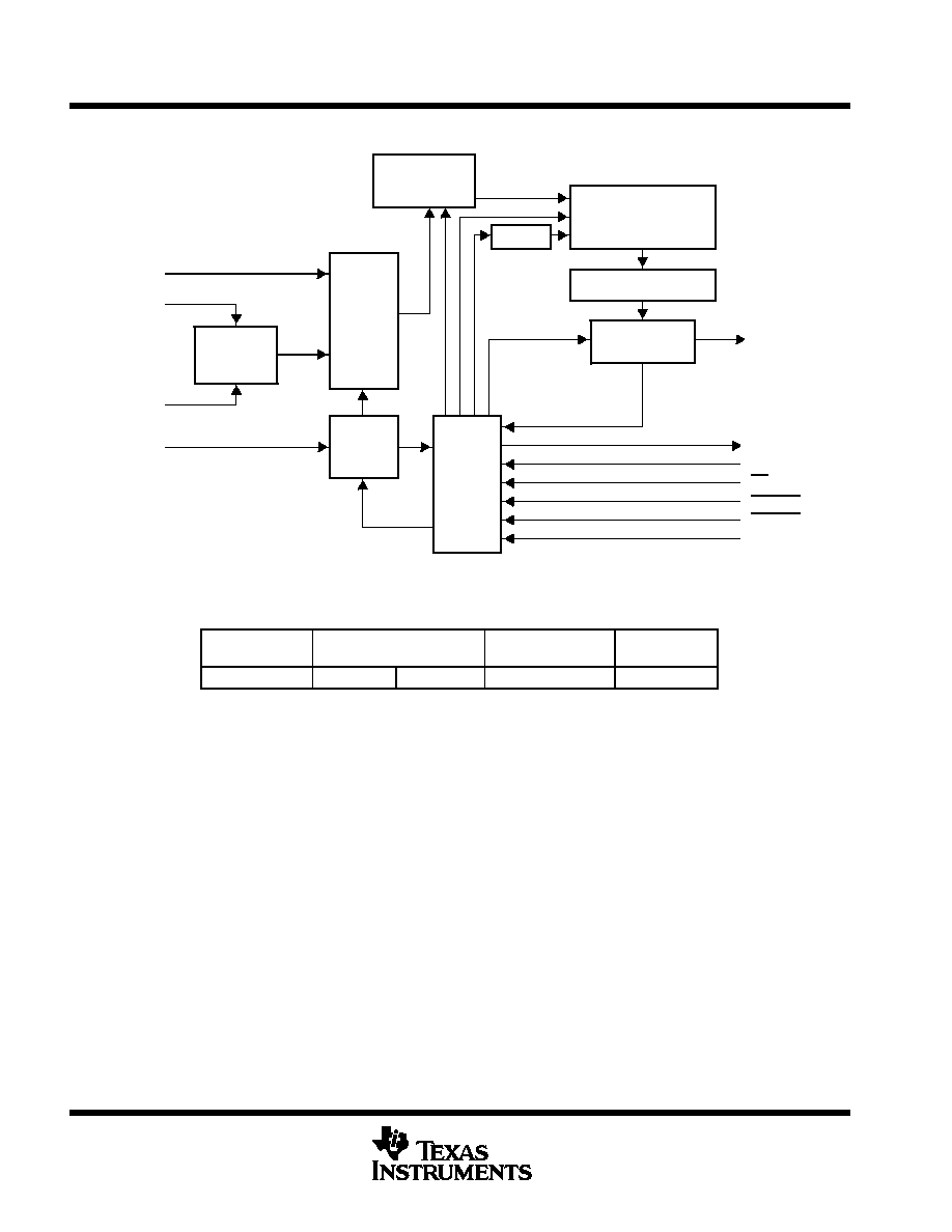
functional block diagram
Analog
MUX
Self-Test
Reference
Input
Data
Register
Control
Logic
and
I/O
Counters
10-Bit ADC
(Switch Capacitors)
Output Data Register
10-to-1
Data Selector
Sample
and
Hold Function
CLOCK
A0≠A7
REF+
REF≠
DATA IN
DATA OUT
EOC
FS
CS
CSTART
INV CLK
I/O CLK
Terminals shown are for the DB package.
1≠8
14
13
17
16
19
12
15
9
11
18
ORDERING INFORMATION
TA
PACKAGE
ORDERABLE
PART NUMBER
TOP-SIDE
MARKING
≠40
∞
C to 125
∞
C
SSOP ≠ DB
Tape and reel
TLV1548QDBREP
1548QE
Package drawings, standard packing quantities, thermal data, symbolization, and PCB design
guidelines are available at www.ti.com/sc/package.

TLV1548-EP
LOW-VOLTAGE 10-BIT ANALOG-TO-DIGITAL CONVERTER
WITH SERIAL CONTROL AND 8 ANALOG INPUTS
SGLS171 ≠ JUNE 2003
3
POST OFFICE BOX 655303
∑
DALLAS, TEXAS 75265
Terminal Functions
TERMINAL
I/O
DESCRIPTION
NAME
NO.
I/O
DESCRIPTION
A0≠A3
A4≠A7
1≠4
5≠8
I
Analog inputs. The analog inputs are internally multiplexed. (For a source impedance greater than
1 k
, the asynchronous start should be used to increase the sampling time.)
CS
15
I
Chip select. A high-to-low transition on CS resets the internal counters and controls and enables DATA IN, DATA
OUT, and I/O CLK within the maximum setup time. A low-to-high transition disables DATA IN, DATA OUT, and I/O
CLK within the setup time.
CSTART
9
I
Sampling/conversion start control. CSTART controls the start of the sampling of an analog input from a selected
multiplex channel. A high-to-low transition starts the sampling of the analog input signal. A low-to-high transition puts
the sample-and-hold function in hold mode and starts the conversion. CSTART is independent from I/O CLK and
works when CS is high. The low CSTART duration controls the duration of the sampling cycle for the switched
capacitor array. CSTART is tied to VCC if not used.
DATA IN
17
I
Serial data input. The 4-bit serial data selects the desired analog input and test voltage to be converted next in a
normal cycle. These bits can also set the conversion rate and enable the power-down mode.
When operating in the microprocessor mode, the input data is presented MSB first and is shifted in on the first four
rising (INV CLK = VCC) or falling (INV CLK = GND) edges of I/O CLK (after CS
).
rising (INV CLK VCC) or falling (INV CLK GND) edges of I/O CLK (after CS
).
When operating in the DSP mode, the input data is presented MSB first and is shifted in on the first four falling (INV
CLK = VCC) or rising (INV CLK = GND) edges of I/O CLK (after FS
).
After the four input data bits have been read into the input data register, DATA IN is ignored for the remainder of the
current conversion period.
DATA OUT
16
O
Three-state serial output of the A/D conversion result. DATA OUT is in the high-impedance state when CS is high
and active when CS is low or after FS
(in DSP mode). With a valid CS signal, DATA OUT is removed from the
high-impedance state and is driven to the logic level corresponding to the MSB or LSB value of the previous
conversion result. DATA OUT changes on the falling (microprocessor mode) or rising (DSP mode) edge of I/O CLK.
EOC
19
O
End of conversion. EOC goes from a high to a low logic level on the tenth rising (microprocessor mode) or tenth
falling (DSP mode) edge of I/O CLK and remains low until the conversion is complete and data is ready for transfer.
EOC can also indicate that the converter is busy.
FS
12
I
DSP frame synchronization input. FS indicates the start of a serial data frame into or out of the device. FS is tied
to VCC when interfacing the device with a microprocessor.
GND
10
Ground return for internal circuitry. All voltage measurements are with respect to GND, unless otherwise noted.
INV CLK
11
I
Inverted clock input. INV CLK is tied to GND when an inverted I/O CLK is used as the source of the input clock. This
affects both microprocessor and DSP interfaces. INV CLK is tied to VCC if I/O CLK is not inverted. INV CLK can also
invoke a built-in test mode.
TLV1548-EP
LOW-VOLTAGE 10-BIT ANALOG-TO-DIGITAL CONVERTER
WITH SERIAL CONTROL AND 8 ANALOG INPUTS
SGLS171 ≠ JUNE 2003
4
POST OFFICE BOX 655303
∑
DALLAS, TEXAS 75265
Terminal Functions (Continued)
TERMINAL
I/O
DESCRIPTION
NAME
NO.
I/O
DESCRIPTION
I/O CLK
18
I
Input/output clock. I/O CLK receives the serial I/O clock input in the two modes and performs the following four
functions in each mode:
Microprocessor mode
∑
When INVCLK = VCC, I/O CLK clocks the four input data bits into the input data register on the first four rising
edges of I/O CLK after CS
with the multiplexer address available after the fourth rising edge. When INV CLK
= GND, input data bits are clocked in on the first four falling edges instead.
∑
On the fourth falling edge of I/O CLK, the analog input voltage on the selected multiplex input begins charging
the capacitor array and continues to do so until the tenth rising edge of I/O CLK except in the extended sampling
cycle where the duration of CSTART determines when to end the sampling cycle.
∑
Output data bits change on the first ten falling I/O clock edges regardless of the condition of INV CLK.
∑
I/O CLK transfers control of the conversion to the internal state machine on the tenth rising edge of I/O CLK
regardless of the condition of INV CLK.
Digital signal processor (DSP) mode
∑
When INV CLK = VCC, I/O CLK clocks the four input data bits into the input data register on the first four falling
edges of I/O CLK after FS
with the multiplexer address available after the fourth falling edges. When INV CLK
= GND, input data bits are clocked in on the first four rising edges instead.
∑
On the fourth rising edge of I/O CLK, the analog input voltage on the selected multiplex input begins charging
the capacitor array and continues to do so until the tenth falling edge of I/O CLK except in the extended sampling
cycle where the duration of CSTART determines when to end the sampling cycle.
∑
Output data MSB shows after FS
and the rest of the output data bits change on the first ten rising I/O CLK edges
regarless of the condition of INV CLK.
∑
I/O CLK transfers control of the conversion to the internal state machine on the tenth falling edge of I/O CLK
regardless of the condition of INV CLK.
REF+
14
I
Upper reference voltage (nominally VCC ). The maximum input voltage range is determined by the difference between
the voltages applied to REF+ and REF≠.
REF≠
13
I
Lower reference voltage (nominally ground)
VCC
20
I
Positive supply voltage
detailed description
Initially, with CS high (inactive), DATA IN and I/O CLK are disabled and DATA OUT is in the high-impedance
state. When the serial interface takes CS low (active), the conversion sequence begins with the enabling of I/O
CLK and DATA IN and the removal of DATA OUT from the high-impedance state. The host then provides the
4-bit channel address to DATA IN and the I/O clock sequence to I/O CLK. During this transfer, the host serial
interface also receives the previous conversion result from DATA OUT. I/O CLK receives an input sequence from
the host that is from 10 to 16 clocks long. The first four valid I/O CLK cycles load the input data register with the
4-bit input data on DATA IN that selects the desired analog channel. The next six clock cycles provide the control
timing for sampling the analog input. Sampling of the analog input is held after the first valid I/O CLK sequence
of ten clocks. The tenth clock edge also takes EOC low and begins the conversion. The exact locations of the
I/O clock edges depend on the mode of operation.
serial interface
The TLV1548 is compatible with generic microprocessor serial interfaces such as SPI and QSPI, and a TMS320
DSP serial interface. The internal latched flag If_mode is generated by sampling the state of FS at the falling
edge of CS. If_mode is set to one (for microprocessor) when FS is high at the falling edge of CS, and If_mode
is cleared to zero (for DSP) when FS is low at the falling edge of CS. This flag controls the multiplexing of I/O
CLK and the state machine reset function. FS is pulled high when interfacing with a microprocessor.
TLV1548-EP
LOW-VOLTAGE 10-BIT ANALOG-TO-DIGITAL CONVERTER
WITH SERIAL CONTROL AND 8 ANALOG INPUTS
SGLS171 ≠ JUNE 2003
5
POST OFFICE BOX 655303
∑
DALLAS, TEXAS 75265
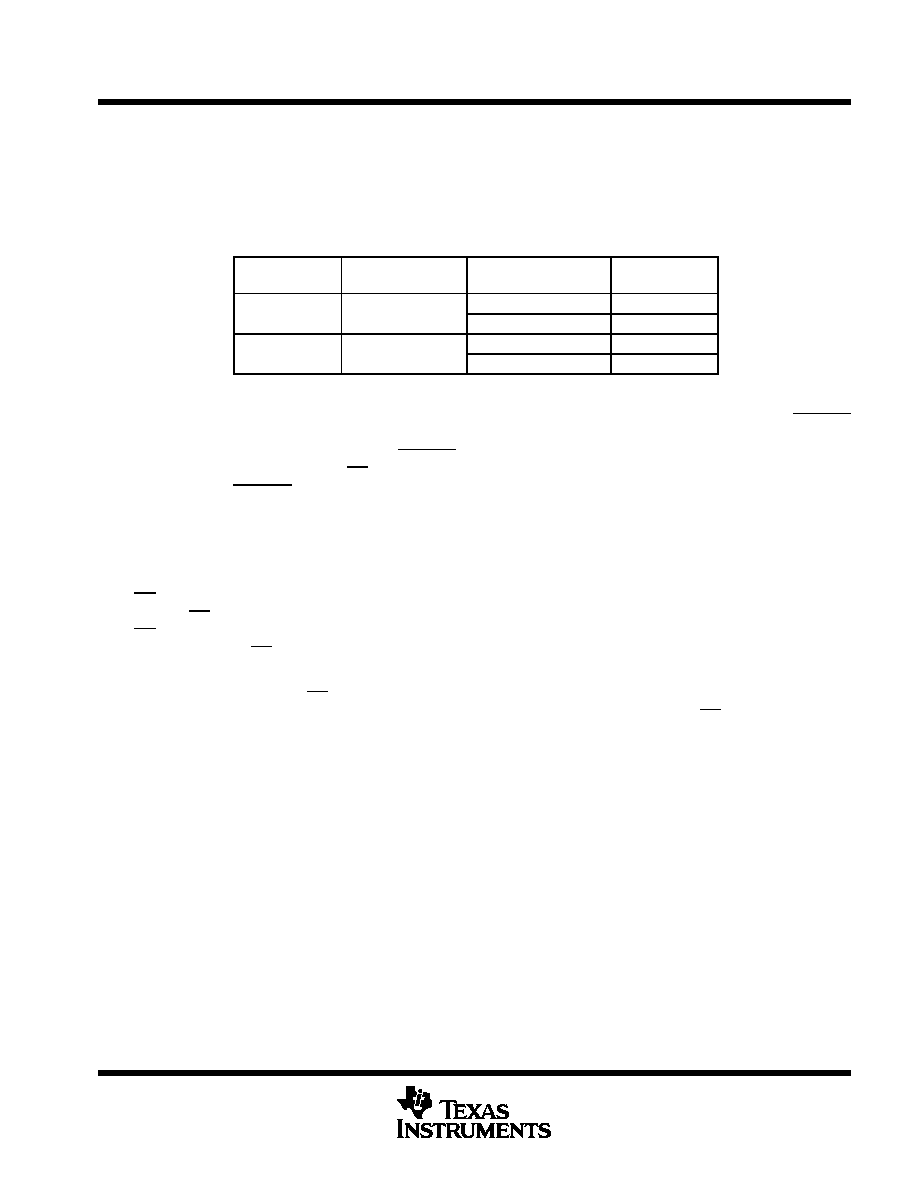
I/O CLK
The I/O CLK can go up to 10 MHz for most of the voltage range when fast I/O is possible. The maximum I/O
CLK is limited to 2.8 MHz for a supply voltage range from 2.7 V. Table 1 lists the maximum I/O CLK frequencies
for all different supply voltage ranges. This also depends on input source impedance. For example, I/O CLK
speed faster than 2.39 MHz is achievable if the input source impedance is less than 1 k
.
Table 1. Maximum I/O CLK Frequency
VCC
MAXIMUM INPUT
RESISTANCE (Max)
SOURCE IMPEDANCE
I/O CLK
2 7 V
5 K
1 k
2.39 MHz
2.7 V
5 K
100
2.81 MHz
4 5 V
1 K
1 k
7.18 MHz
4.5 V
1 K
100
10 MHz
microprocessor serial interface
Input data bits from DATA IN are clocked in on the first four rising edges of the I/O CLK sequence if INV CLK
is held high when the device is in microprocessor interface mode. Input data bits are clocked in on the first four
falling edges of the I/O CLK sequence if INV CLK is held low. The MSB of the previous conversion appears on
DATA OUT on the falling edge of CS. The remaining nine bits are shifted out on the next nine edges (depending
on the state of INV CLK) of I/O CLK. Ten bits of data are transmitted to the host through DATA OUT.
A minimum of 9.5 clock pulses is required for the conversion to begin. On the tenth clock rising edge, the EOC
output goes low and returns to the high logic level when the conversion is complete; then the result can be read
by the host. On the tenth clock falling edge, the internal logic takes DATA OUT low to ensure that the remaining
bit values are zero if the I/O CLK transfer is more than ten clocks long.
CS is inactive (high) between serial I/O CLK transfers. Each transfer takes at least ten I/O CLK cycles. The falling
edge of CS begins the sequence by removing DATA OUT from the high-impedance state. The rising edge of
CS ends the sequence by returning DATA OUT to the high-impedance state within the specified delay time. Also,
the rising edge of CS disables I/O CLK and DATA IN within a setup time. A conversion does not begin until the
tenth I/O CLK rising edge.
A high-to-low transition on CS within the specified time during an ongoing cycle aborts the cycle, and the device
returns to the initial state (the output data register holds the previous conversion result). CS should not be taken
low close to completion of conversion because the output data can be corrupted.