 | –≠–ª–µ–∫—Ç—Ä–æ–Ω–Ω—ã–π –∫–æ–º–ø–æ–Ω–µ–Ω—Ç: TLV2625 | –°–∫–∞—á–∞—Ç—å:  PDF PDF  ZIP ZIP |

TLV2620, TLV2621, TLV2622, TLV2623, TLV2624, TLV2625, TLV262xA
FAMILY OF LOW-POWER WIDE BANDWIDTH SINGLE SUPPLY
OPERATIONAL AMPLIFIERS WITH SHUTDOWN
SLOS251B ≠ DECEMBER 2000 ≠ REVISED APRIL 2001
1
POST OFFICE BOX 655303
∑
DALLAS, TEXAS 75265
D
CMOS Rail-To-Rail Output
D
V
ICR
Includes Positive Rail
D
Wide Bandwidth . . . 11 MHz
D
Slew Rate . . . 10 V/
µ
s
D
Supply Current . . . 800
µ
A/Channel
D
Input Noise Voltage . . . 27 nV/
Hz
D
Ultralow Power Down Mode
≠ I
DD(SHDN
) = 4
µ
A/Channel
D
Supply Voltage Range . . . 2.7 V to 5.5 V
D
Specified Temperature Range
≠ ≠40 C to 125 C . . . Industrial Grade
D
Ultrasmall Packaging
≠ 5 or 6 Pin SOT-23 (TLV2620/1)
≠ 8 or 10 Pin MSOP (TLV2622/3)
D
Universal Opamp EVM (See SLOU060 for
More Information)
description
The TLV262x single supply operational amplifiers
provide rail-to-rail output with an input range that
includes the positive rail. The TLV262x takes the minimum operating supply voltage down to 2.7 V over the
extended industrial temperature range (≠40
∞
C to 125
∞
C) while adding the rail-to-rail output swing feature. The
TLV262x also provides 11-MHz bandwidth from only 800
µ
A of supply current. The maximum recommended
supply voltage is 5.5 V, which, when coupled with a 2.7-V minimum, allows the devices to be operated from
lithium ion cells.
The combination of wide bandwidth, low noise, and low distortion makes it ideal for high speed and high
resolution data converter applications. The positive input range allows it to directly interface to positive rail
referred systems.
All members are available in PDIP and SOIC with the singles in the small SOT-23 package, duals in the MSOP,
and quads in the TSSOP package.
The 2.7-V operation makes it compatible with Li-Ion powered systems and the operating supply voltage range
of many micro-power micro-controllers available today including TI's MSP430.
AMPLIFIER SELECTION TABLE
DEVICE
VDD
[V]
IDD/ch
[
µ
A]
VIO
[
µ
V]
IIB
[pA]
VICR
[V]
GBW
[MHz]
SLEW RATE
[V/
µ
s]
Vn, 1 kHz
[nV/
Hz]
IO
[mA]
SHUT-
DOWN
TLV262x
2.7≠5.5
750
250
1
1 V to VDD + 0.2
11
10
27
28
Y
TLV263x
2.7≠5.5
750
250
1
GND to VDD ≠ 0.8
10
9
27
28
Y
TLV278x
1.8≠3.6
650
250
2.5
≠0.2 to VDD + 0.2
8
5
9
10
Y
TLC07x
4.5 ≠ 16
1900
60
1.5
0.5 to VDD ≠ 0.8
10
19
7
55
Y
TLC08x
4.5 ≠ 16
1900
60
3
GND to VDD ≠ 1
10
19
8.5
55
Y
This device is in the Product Preview stage of development. Contact your local TI sales office for availability.
Please be aware that an important notice concerning availability, standard warranty, and use in critical applications of
Texas Instruments semiconductor products and disclaimers thereto appears at the end of this data sheet.
PRODUCTION DATA information is current as of publication date.
Products conform to specifications per the terms of Texas Instruments
standard warranty. Production processing does not necessarily include
testing of all parameters.
Copyright
2001, Texas Instruments Incorporated
Operational Amplifier
+
≠
≠10
0
10
20
30
40
50
60
70
80
90
100
110
120
f ≠ Frequency ≠ Hz
10
1k
10M
10k
100k
100
1M
150
120
90
60
30
0
≠30
≠60
≠90
Phase Margin ≠
∞
DIFFERENTIAL VOLTAGE AMPLIFICATION AND PHASE
vs
FREQUENCY
≠ Differential V
oltage
Amplification ≠ dB
A
VD
Gain
Phase
180
VDD = 2.7 V and 5 V
RL= 2 k
CL = 10 pF
TA = 25
∞
C
TLV2620, TLV2621, TLV2622, TLV2623, TLV2624, TLV2625, TLV262xA
FAMILY OF LOW-POWER WIDE BANDWIDTH SINGLE SUPPLY
OPERATIONAL AMPLIFIERS WITH SHUTDOWN
SLOS251B ≠ DECEMBER 2000 ≠ REVISED APRIL 2001
2
POST OFFICE BOX 655303
∑
DALLAS, TEXAS 75265
TLV2620 and TLV2621 AVAILABLE OPTIONS
V
PACKAGED DEVICES
TA
VIOmax
AT 25
∞
C
SMALL OUTLINE
SOT-23
PLASTIC DIP
AT 25 C
(D)
(DBV)
SYMBOL
(P)
- 40
∞
C to 125
∞
C
3500
µ
V
TLV2620ID
TLV2621ID
TLV2620IDBV
TLV2621IDBV
VBAI
VBBI
TLV2620IP
TLV2621IP
This package is available taped and reeled. To order this packaging option, add an R suffix to the part number (e.g., TLV2620IDR).
The SOT23 package devices are only available taped and reeled. The R Suffix denotes quantities (3,000 pieces per reel). For smaller quantities
(250 pieces per mini-reel), add a T suffix to the part number (e.g. TLV2620IDBVT).
TLV2622 and TLV2623 AVAILABLE OPTIONS
PACKAGED DEVICES
TA
VIOmax
AT 25
∞
C
SMALL
OUTLINE
MSOP
PLASTIC
DIP
PLASTIC
DIP
AT 25 C
OUTLINE
(D)
(DGK)
SYMBOL
(DGS)
SYMBOL
DIP
(N)
DIP
(P)
≠ 40
∞
C to 125
∞
C
3500
µ
V
TLV2622ID
TLV2623ID
TLV2622IDGK
--
xxTIAKM
--
--
TLV2623IDGS
--
xxTIALC
--
TLV2623IN
TLV2622IP
--
This package is available taped and reeled. To order this packaging option, add an R suffix to the part number (e.g., TLV2622IDR).
TLV2624 and TLV2625 AVAILABLE OPTIONS
V
ma
PACKAGED DEVICES
TA
VIOmax
AT 25
∞
C
SMALL OUTLINE
(D)
PLASTIC DIP
(N)
TSSOP
(PW)
≠ 40
∞
C to 125
∞
C
3500
µ
V
TLV2624ID
TLV2625ID
TLV2624IN
TLV2625IN
TLV2624IPW
TLV2625IPW
This package is available taped and reeled. To order this packaging option, add an R suffix to the part number
(e.g., TLV2624IDR).
TLV2620, TLV2621, TLV2622, TLV2623, TLV2624, TLV2625, TLV262xA
FAMILY OF LOW-POWER WIDE BANDWIDTH SINGLE SUPPLY
OPERATIONAL AMPLIFIERS WITH SHUTDOWN
SLOS251B ≠ DECEMBER 2000 ≠ REVISED APRIL 2001
3
POST OFFICE BOX 655303
∑
DALLAS, TEXAS 75265
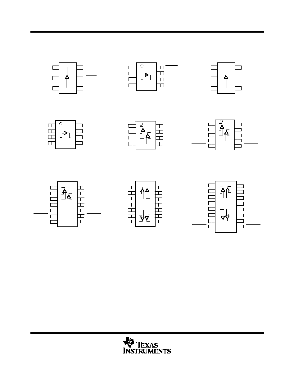
TLV262x PACKAGE PINOUTS
3
2
4
5
(TOP VIEW)
1
OUT
GND
IN+
VDD
IN ≠
TLV2621
DBV PACKAGE
1
2
3
4
5
10
9
8
7
6
1OUT
1IN ≠
1IN+
GND
1SHDN
V
DD
2OUT
2IN ≠
2IN+
2SHDN
3
2
4
6
(TOP VIEW)
1
OUT
GND
IN+
VDD
IN ≠
TLV2620
DBV PACKAGE
5
SHDN
TLV2623
DGS PACKAGE
(TOP VIEW)
NC ≠ No internal connection
1
2
3
4
8
7
6
5
NC
IN ≠
IN +
GND
SHDN
V
DD
OUT
NC
TLV2620
D OR P PACKAGE
(TOP VIEW)
1
2
3
4
8
7
6
5
NC
IN ≠
IN +
GND
NC
V
DD
OUT
NC
TLV2621
D OR P PACKAGE
(TOP VIEW)
1
2
3
4
5
6
7
14
13
12
11
10
9
8
1OUT
1IN ≠
1IN+
GND
NC
1SHDN
NC
V
DD
2OUT
2IN ≠
2IN+
NC
2SHDN
NC
(TOP VIEW)
TLV2623
D OR N PACKAGE
1
2
3
4
5
6
7
14
13
12
11
10
9
8
1OUT
1IN ≠
1IN+
V
DD
2IN+
2IN ≠
2OUT
4OUT
4IN ≠
4IN+
GND
3IN+
3IN ≠
3OUT
(TOP VIEW)
TLV2624
D, N, OR PW PACKAGE
1
2
3
4
5
6
7
8
16
15
14
13
12
11
10
9
1OUT
1IN ≠
1IN+
V
DD
2IN+
2IN ≠
2OUT
1SHDN
4OUT
4IN ≠
4IN+
GND
3IN +
3IN≠
3OUT
2SHDN
(TOP VIEW)
TLV2625
D, N, OR PW PACKAGE
1
2
3
4
8
7
6
5
1OUT
1IN ≠
1IN +
GND
V
DD
2OUT
2IN ≠
2IN+
TLV2622
D, DGK, OR P PACKAGE
(TOP VIEW)

TLV2620, TLV2621, TLV2622, TLV2623, TLV2624, TLV2625, TLV262xA
FAMILY OF LOW-POWER WIDE BANDWIDTH SINGLE SUPPLY
OPERATIONAL AMPLIFIERS WITH SHUTDOWN
SLOS251B ≠ DECEMBER 2000 ≠ REVISED APRIL 2001
4
POST OFFICE BOX 655303
∑
DALLAS, TEXAS 75265
absolute maximum ratings over operating free-air temperature range (unless otherwise noted)
Supply voltage, V
DD
(see Note 1)
6 V
. . . . . . . . . . . . . . . . . . . . . . . . . . . . . . . . . . . . . . . . . . . . . . . . . . . . . . . . . . . . .
Differential input voltage, V
ID
±
V
DD
. . . . . . . . . . . . . . . . . . . . . . . . . . . . . . . . . . . . . . . . . . . . . . . . . . . . . . . . . . . . . . .
Input voltage range, V
I
(see Note 1)
1 to V
DD
+0.2 V
. . . . . . . . . . . . . . . . . . . . . . . . . . . . . . . . . . . . . . . . . . . . . . . .
Input current, I
I
(any input)
±
10 mA
. . . . . . . . . . . . . . . . . . . . . . . . . . . . . . . . . . . . . . . . . . . . . . . . . . . . . . . . . . . . . . .
Output current, I
O
±
40 mA
. . . . . . . . . . . . . . . . . . . . . . . . . . . . . . . . . . . . . . . . . . . . . . . . . . . . . . . . . . . . . . . . . . . . . . .
Continuous total power dissipation
See Dissipation Rating Table
. . . . . . . . . . . . . . . . . . . . . . . . . . . . . . . . . . . . .
Operating free-air temperature range, T
A
: I suffix
≠40
∞
C to 125
∞
C
. . . . . . . . . . . . . . . . . . . . . . . . . . . . . . . . . . . .
Maximum junction temperature, T
J
150
∞
C
. . . . . . . . . . . . . . . . . . . . . . . . . . . . . . . . . . . . . . . . . . . . . . . . . . . . . . . . .
Storage temperature range, T
stg
≠ 65
∞
C to 150
∞
C
. . . . . . . . . . . . . . . . . . . . . . . . . . . . . . . . . . . . . . . . . . . . . . . . . . .
Lead temperature 1,6 mm (1/16 inch) from case for 10 seconds
260
∞
C
. . . . . . . . . . . . . . . . . . . . . . . . . . . . . . .
Stresses beyond those listed under "absolute maximum ratings" may cause permanent damage to the device. These are stress ratings only, and
functional operation of the device at these or any other conditions beyond those indicated under "recommended operating conditions" is not
implied. Exposure to absolute-maximum-rated conditions for extended periods may affect device reliability.
NOTE 1: All voltage values, except differential voltages, are with respect to GND.
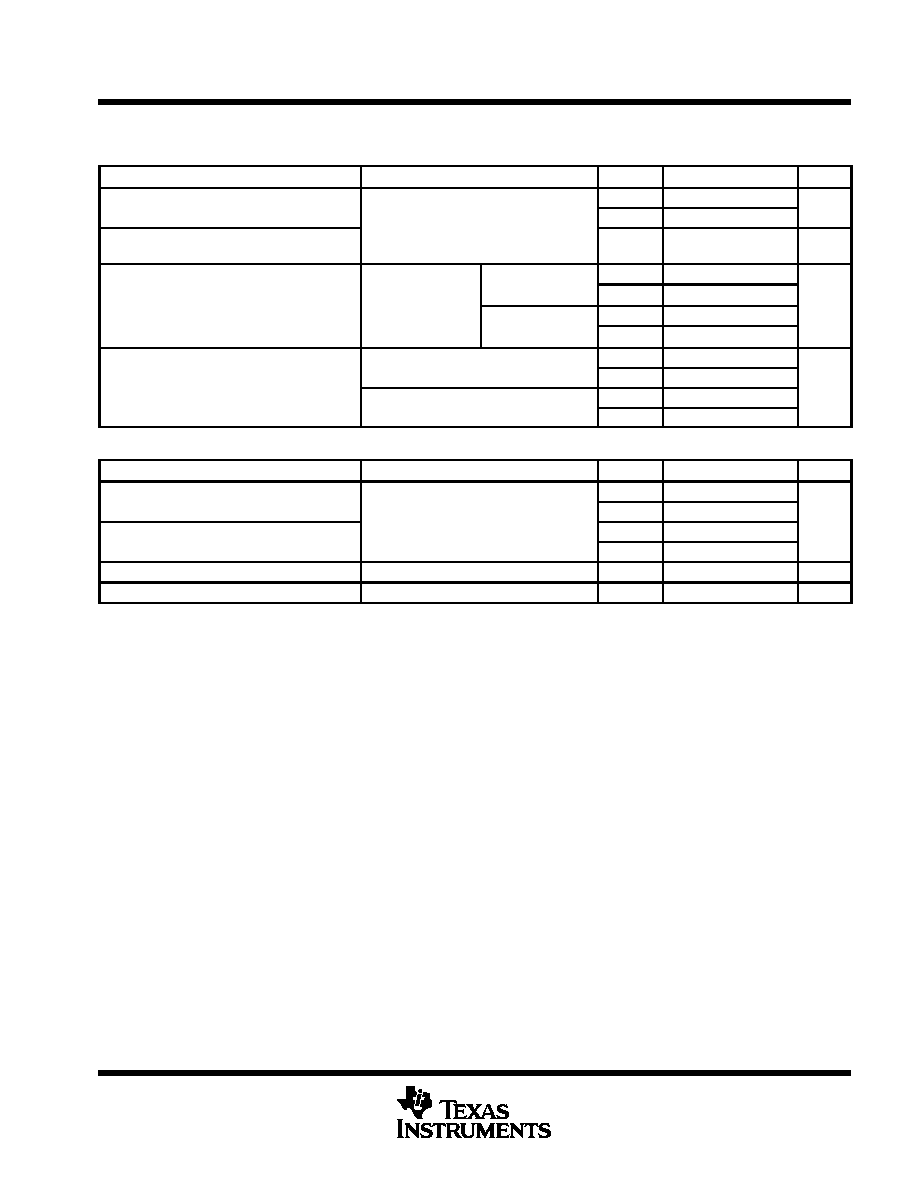
DISSIPATION RATING TABLE
PACKAGE
JC
JA
TA
25
∞
C
TA = 125
∞
C
PACKAGE
JC
(
∞
C/W)
JA
(
∞
C/W)
A
POWER RATING
A
POWER RATING
D (8)
38.3
176
710 mW
142 mW
D (14)
26.9
122.3
1022 mW
204.4 mW
D (16)
25.7
114.7
1090 mW
218 mW
DBV (5)
55
324.1
385 mW
77.1 mW
DBV (6)
55
294.3
425 mW
85 mW
DGK (8)
54.2
259.9
481 mW
96.1 mW
DGS (10)
54.1
259.7
485 mW
97 mW
N (14, 16)
32
78
1600 mW
320.5 mW
P (8)
41
104
1200 mW
240.4 mW
PW (14)
29.3
173.6
720 mW
144 mW
PW (16)
28.7
161.4
774 mW
154.9 mW
recommended operating conditions
MIN
MAX
UNIT
Supply voltage VDD
Single supply
2.7
5.5
V
Supply voltage, VDD
Split supply
±
1.35
±
2.75
V
Common-mode input voltage range, VICR
1
VDD+0.2
V
Operating free-air temperature, TA
I-suffix
≠ 40
125
∞
C
Shutdown on/off voltage level
VIL
0.4
V
Shutdown on/off voltage level
VIH
2
V
Relative to GND.
TLV2620, TLV2621, TLV2622, TLV2623, TLV2624, TLV2625, TLV262xA
FAMILY OF LOW-POWER WIDE BANDWIDTH SINGLE SUPPLY
OPERATIONAL AMPLIFIERS WITH SHUTDOWN
SLOS251B ≠ DECEMBER 2000 ≠ REVISED APRIL 2001
5
POST OFFICE BOX 655303
∑
DALLAS, TEXAS 75265
electrical characteristics at specified free-air temperature, V
DD
= 2.7 V, 5 V (unless otherwise noted)
dc performance
PARAMETER
TEST CONDITIONS
TA
MIN
TYP
MAX
UNIT
VIO
Input offset voltage
V
V
/2
25
∞
C
250
3500
µ
V
VIO
Input offset voltage
VIC = VDD/2,
VO = VDD/2
Full range
4500
µ
V
VIO
Temperature coefficient of input offset
voltage
VO = VDD/2,
RS = 50
25
∞
C
3
µ
V/
∞
C
VDD = 2 7 V
25
∞
C
77
98
CMRR
Common-mode rejection ratio
VIC = 1 to VDD,
VDD = 2.7 V
Full range
73
dB
CMRR
Common-mode rejection ratio
IC
DD
RS = 50
VDD = 5 V
25
∞
C
78
99
dB
VDD = 5 V
Full range
75
VDD = 2 7 V RL = 2 k
VO(PP) = 1 7 V
25
∞
C
90
100
AVD
Large-signal differential voltage
VDD = 2.7 V, RL = 2 k
, VO(PP) = 1.7 V
Full range
82
dB
AVD
g
g
g
amplification
VDD = 5 V RL = 2 k
VO(PP) = 4 V
25
∞
C
95
100
dB
VDD = 5 V, RL = 2 k
, VO(PP) = 4 V
Full range
90
input characteristics
PARAMETER
TEST CONDITIONS
TA
MIN
TYP
MAX
UNIT
IIO
Input offset current
25
∞
C
1
50
IIO
Input offset current
VIC = VDD/2,
VO VDD/2
Full range
100
pA
IIB
Input bias current
VO = VDD/2,
RS = 50
25
∞
C
1
50
pA
IIB
Input bias current
RS = 50
Full range
200
ri(d)
Differential input resistance
25
∞
C
100
G
Ci(c)
Common-mode input capacitance
f = 1 kHz
25
∞
C
8
pF
Full range is ≠40
∞
C to 125
∞
C for the I suffix.