
TLV320AIC1103
SLAS356 ≠ DECEMBER 2001
PCM CODEC
1
www.ti.com
FEATURES
D
2.7-V Operation
D
Two Differential Microphone Inputs, One
Differential Earphone Output, and One
Single-Ended Earphone Output
D
Programmable Gain Amplifiers for Transmit,
Receive, Sidetone, and Volume Control
D
Earphone Mute and Microphone Mute
D
On-Chip I
2
C Bus, Which Provides a Simple,
Standard, Two-Wire Serial Interface With
Digital ICs
D
Programmable for 15-Bit Linear Data or 8-Bit
Companded (
µ
-Law or A-Law) Data
D
Available in a 32-Pin Thin Quad Flatpack
(TQFP) Package and an 80-Pin GQE MicroStar
Junior
t
Ball Grid Array (BGA)
D
Designed for Analog and Digital Wireless
Handsets and Telecommunications
Applications
D
Dual-Tone Multifrequency (DTMF) and Single
Tone Generator
D
Pulse Density Modulated (PDM) Buzzer
Output
APPLICATIONS
D
Digital Handset
D
Digital Headset
D
Cordless Phones
D
Digital PABX
D
Digital Voice Recording
DESCRIPTION
The PCM codec is designed to perform transmit
encoding analog/digital (A/D) conversion, receive
decoding digital/analog (D/A) conversion, and transmit
and receive filtering for voice-band communications
systems. The device operates in either the 15-bit linear
or 8-bit companded
(µ
-law or A-Law) mode, which is
selectable through the I
2
C interface. The PCM codec
generates its own internal clocks from a 2.048-MHz
master clock input.
PBS PACKAGE
(TOP VIEW)
31
30
29
28
27
9
10
PCMO
PCMI
DV
SS
DV
DD
SCL
SDA
NC
NC
PLLV
DD
EARV
SS
EAR1ON
EARV
DD
EAR1OP
EARV
SS
EAR2O
AV
DD
32
26
11
12
13
14
15
MBIAS
MIC1P
MIC1N
MIC2P
NC
16
25
1
2
3
4
5
6
7
8
24 23 22 21 20 19 18 17
MIC2N
REXT
AV
SS
MCLK
PLL
V
SS
V
SS
RESET
PWRUPSEL
BUZZCON
PCMSYN
PCMCLK
NC ≠ No internal connection
This device contains circuits to protect its inputs and outputs against damage due to high static voltages or electrostatic fields. These
circuits have been qualified to protect this device against electrostatic discharges (ESD) of up to 2 kV according to MIL-STD-883C,
Method 3015; however, it is advised that precautions be taken to avoid application of any voltage higher than maximum-rated
voltages to these high-impedance circuits. During storage or handling, the device leads should be shorted together or the device
should be placed in conductive foam. In a circuit, unused inputs should always be connected to an appropriated logic voltage level,
preferably either VCC or ground. Specific guidelines for handling devices of this type are contained in the publication Guidelines for
Handling Electrostatic-Discharge-Sensitive (ESDS) Devices and Assemblies available from Texas Instruments.
PRODUCTION DATA information is current as of publication date.
Products conform to specifications per the terms of Texas Instruments
standard warranty. Production processing does not necessarily include
testing of all parameters.
MicroStar Junior is a trademark of Texas Instruments.
All other trademarks are the property of their respective owners.
Copyright
2001, Texas Instruments Incorporated

TLV320AIC1103
SLAS356 ≠ DECEMBER 2001
2
www.ti.com
9
8
7
6
5
A
B
C
D
E
F
3
2
1
G
H
J
4
AVDD
BUZZCON
PCMSYN
PCMCLK
PCMO
MBIAS
RESET
MCLK
PWRUPSEL
AVSS
MIC2P
MIC1P
MIC1N
REXT
MIC2N
NC
NC
NC
NC
NC
NC
NC
NC
NC
NC
NC
NC
NC
NC
NC
NC
NC
NC
NC
NC
NC
NC
NC
NC
NC
NC
VSS
NC
NC
NC
NC
NC
NC
NC
NC
NC
NC
NC
NC
NC
NC
NC
NC
NC
NC
NC
NC
NC
NC
PLL
V
SS
PLL
V
DD
EAR
V
SS
EAR1ON
EAR1OP
EAR
V
SS
EAR2O
SDA
SCL
DV
DD
DV
SS
PCMI
MicroStar Junior
(GQE) PACKAGE
(TOP VIEW)
EAR
V
DD
NC
NC
NC
TLV320AIC1103
SLAS356 ≠ DECEMBER 2001
3
www.ti.com
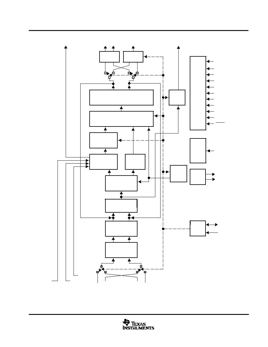
functional block diagram
PCMI (15)
PCMSYN (18)
PCMCLK (17)
MIC1P (2)
MIC1N (3)
MIC2P (4)
MIC2N (5)
MIC
Amplifier 1
g = 23.5 dB
MIC
Amplifier 2
g = 12 dB
or 0 dB
Analog
Modulator
TX Filter
and PGA
g = ≠10 dB
to 0 dB
PCM
Interface
Sidetone
g = ≠24 dB
to
≠12 dB
RX
Control
g = ≠18 dB
to 0 dB
RX Filter
and PGA
g = ≠6 dB
to +6 dB
Digital
Modulator
and Filter
Ear
Amp1
Ear
Amp2
DTMF
Generator
Control Bus
I 2 C
I/F
REF
PLL
Buzzer
Control
Power
SCL
SDA
MBIAS
REXT
MCLK
RESET
SS
EARV
DD
EARV
SS
PLLV
DD
PLLV
SS
DV
DD
DV
SS
AV
DD
AV
SS
V
PWRUPSEL (20)
PCMO (16)
EAR1OP (29) EAR1ON (27) EAR2O (31)
BUZZCON (19)
Volume
and
RESET
(23)
(32)
(8)
(13)
(14)
(25)
(24)
(28)
(30, 26)
(21)
(22)
(6)
(1)
(11)
(12)

TLV320AIC1103
SLAS356 ≠ DECEMBER 2001
4
www.ti.com
functional description
power on/reset
The power for the various digital and analog circuits is separated to improve the noise performance of the
device. An external reset must be applied to the active low RESET terminal to assure reset upon power on. After
the initial power-on sequence the TLV320AIC1103 can be functionally powered up and down by writing to the
power control register through the I
2
C interface. There is a hardwired selectable power-up terminal in default
mode option. The PWRUPSEL function allows the VBAP to power up in the default mode and allows use without
a microcontroller.
reference
A precision band gap reference voltage is generated internally and supplies all required voltage references to
operate the transmit and receive channels. The reference system also supplies bias voltage for use with an
electret microphone at terminal MBIAS. An external precision resistor is required for reference current setting
at terminal REXT.
control interface
The I
2
C interface is a two-wire bidirectional serial interface that controls the PCM codec by writing data to the
six control registers:
D
Power control
D
Mode control
D
Transmit PGA and sidetone control
D
Receive PGA gain and volume control
D
DTMF high tone
D
DTMF low tone
There are two power-up modes which may be selected at the PWRUPSEL terminal:
D
The PWRUPSEL state (V
DD
at terminal 20) causes the device to power up in the default mode when power
is applied. In the default mode, the I
2
C interface is not required, and the device may be used without an I
2
C
interface. The programmable functions are fixed in the default modes.
D
The PWRUPSEL state (ground at terminal 20) causes the device to go to a power-down state when power
is applied. In this mode an I
2
C interface is required to power up the device.
phase-locked loop
The internal digital filters and modulators require a 10.24-MHz clock that is generated by phase locking to the
2.048-MHz master clock input.
PCM interface
The PCM interface transmits and receives data at the PCMO and PCMI terminals respectively. The data is
transmitted or received at the PCMCLK speed once every PCMSYN cycle. The PCMCLK can be tied directly
to the 2.048-MHz master clock (MCLK). The PCMSYN can be driven by an external source or derived from the
master clock and used as an interrupt to the host controller.
microphone amplifiers
The microphone input is a switchable interface for two differential microphone inputs. The first stage is a low-
noise differential amplifier that provides a gain of 23.5 dB. The second stage amplifier has a selectable gain of
0 dB or 12 dB.

TLV320AIC1103
SLAS356 ≠ DECEMBER 2001
5
www.ti.com
functional description (continued)
analog modulator
The transmit channel modulator is a third-order sigma-delta design.
transmit filter and PGA
The transmit filter is a digital filter designed to meet CCITT G.714 requirements. The device operates in either
the 15-bit linear or 8-bit companded
µ
-law or A-law mode that is selectable through the I
2
C interface. The
transmit PGA defaults to 0 dB.
sidetone
A portion of the transmitted audio is attenuated and fed back to the receive channel through the sidetone path.
The sidetone path defaults to ≠12 dB. The sidetone path can be enabled by writing to the power control register.
receive volume control
The receive volume control block acts as an attenuator with a range of ≠18 dB to 0 dB in 2 dB steps for control
of the receive channel volume. The receive volume control gain defaults to 0 dB.
receive filter and PGA
The receive filter is a digital filter that meets CCITT G.714 requirements with a high-pass filter that is selectable
through the I
2
C interface. The device operates in either the 15-bit linear or 8-bit
µ
-law or A-law companded
mode, which is selectable through the I
2
C interface. The gain defaults to ≠1 dB representing a 3-dBm0 level
for a 32-
load impedance and the corresponding digital full scale PCMI code. The gain may be set to ≠2 dB
for the respective 3-dBm0 level for a 16-
load impedance.
digital modulator and filter
The second-order digital modulator and filter convert the received digital PCM data to the analog output required
by the earphone interface.
earphone amplifiers
The analog signal can be routed to either of two earphone amplifiers, one with differential output (EAR1ON and
EAR1OP) and one with single-ended output (EAR2O). Clicks and pops are suppressed for EAR1 differential
output only.
tone generator
The tone generator provides generation of standard DTMF tones and single tone frequencies which are output
to the following devices: 1) the buzzer driver, as a pulse density modulation (PDM) signal, and 2) the receive
path digital/analog converter (DAC) for outputting through the earphone. There are 255 possible single tones.
The tone integer value is determined by the following formula:
Round (Tone Freq (Hz)/7.8135 Hz)
The value is loaded into one of two 8-bit registers, the high-tone register (04), or the low-tone register (05). The
tone output is 2 dB higher when applied to the high-tone register (04). When generating DTMF tones, the high
DTMF tone must be applied to the high-tone register and the low frequency tone to the low-tone register.