 | –≠–ª–µ–∫—Ç—Ä–æ–Ω–Ω—ã–π –∫–æ–º–ø–æ–Ω–µ–Ω—Ç: TLV5616C | –°–∫–∞—á–∞—Ç—å:  PDF PDF  ZIP ZIP |
TLV5616C, TLV5616I
2.7 V TO 5.5 V LOW POWER 12-BIT DIGITAL-TO-ANALOG
CONVERTERS WITH POWER DOWN
SLAS152B ≠ DECEMBER 1997 ≠ REVISED MARCH 1999
1
POST OFFICE BOX 655303
∑
DALLAS, TEXAS 75265
D
12-Bit Voltage Output DAC
D
Programmable Settling Time vs Power
Consumption
3
µ
s in Fast Mode
9
µ
s in Slow Mode
D
Ultra Low Power Consumption:
900
µ
W Typ in Slow Mode at 3 V
2.1 mW Typ in Fast Mode at 3 V
D
Differential Nonlinearity . . . <0.5 LSB Typ
D
Compatible With TMS320 and SPI Serial
Ports
D
Power-Down Mode (10 nA)
D
Buffered High-Impedance Reference Input
D
Voltage Output Range . . . 2 Times the
Reference Input Voltage
D
Monotonic Over Temperature
D
Available in MSOP Package
applications
D
Digital Servo Control Loops
D
Digital Offset and Gain Adjustment
D
Industrial Process Control
D
Machine and Motion Control Devices
D
Mass Storage Devices
description
The TLV5616 is a 12-bit voltage output
digital-to-analog converter (DAC) with a flexible
4-wire serial interface. The 4-wire serial interface
allows glueless interface to TMS320, SPI, QSPI,
and Microwire serial ports. The TLV5616 is
programmed with a 16-bit serial string containing
4 control and 12 data bits. Developed for a wide
range of supply voltages, the TLV5616 can
operate from 2.7 V to 5.5 V.
The resistor string output voltage is buffered by a x2 gain rail-to-rail output buffer. The buffer features a Class AB
output stage to improve stability and reduce settling time. The settling time of the DAC is programmable to allow
the designer to optimize speed versus power dissipation. The settling time is chosen by the control bits within
the 16-bit serial input string. A high-impedance buffer is integrated on the REFIN terminal to reduce the need
for a low source impedance drive to the terminal.
Implemented with a CMOS process, the TLV5616 is designed for single supply operation from 2.7 V to 5.5 V.
The device is available in an 8-terminal SOIC package. The TLV5616C is characterized for operation from 0
∞
C
to 70
∞
C. The TLV5616I is characterized for operation from ≠ 40
∞
C to 85
∞
C.
AVAILABLE OPTIONS
PACKAGE
TA
SMALL OUTLINE
(D)
MSOP
(DGK)
PLASTIC DIP
(P)
0
∞
C to 70
∞
C
TLV5616CD
TLV5616CDGK
TLV5616CP
≠ 40
∞
C to 85
∞
C
TLV5616ID
TLV5616IDGK
TLV5616IP
Available in tape and reel as the TLV5616CDR and the TLV5616IDR
Please be aware that an important notice concerning availability, standard warranty, and use in critical applications of
Texas Instruments semiconductor products and disclaimers thereto appears at the end of this data sheet.
Copyright
©
1999, Texas Instruments Incorporated
PRODUCTION DATA information is current as of publication date.
Products conform to specifications per the terms of Texas Instruments
standard warranty. Production processing does not necessarily include
testing of all parameters.
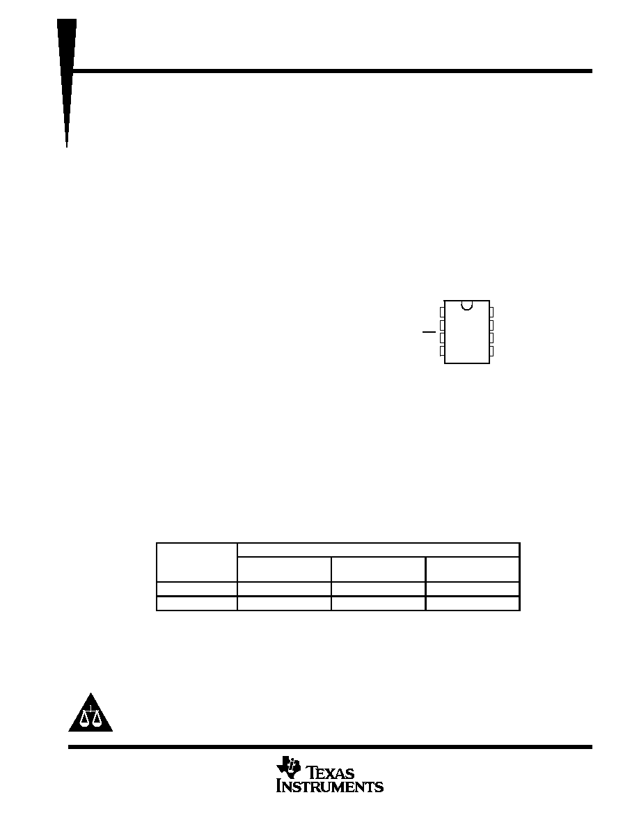
1
2
3
4
8
7
6
5
DIN
SCLK
CS
FS
V
DD
OUT
REFIN
AGND
D, DGK, OR P PACKAGE
(TOP VIEW)
TLV5616C, TLV5616I
2.7 V TO 5.5 V LOW POWER 12-BIT DIGITAL-TO-ANALOG
CONVERTERS WITH POWER DOWN
SLAS152B ≠ DECEMBER 1997 ≠ REVISED MARCH 1999
2
POST OFFICE BOX 655303
∑
DALLAS, TEXAS 75265
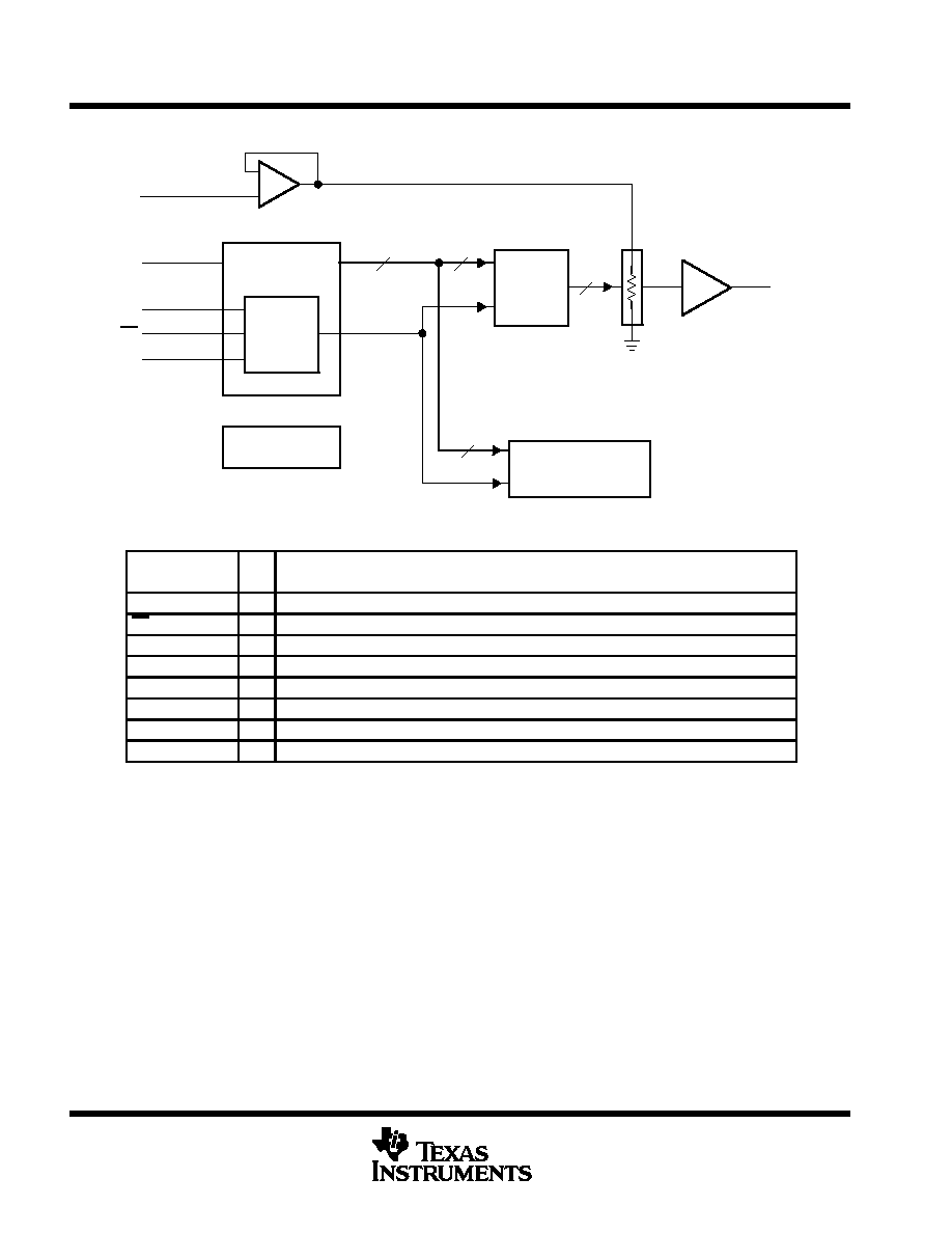
functional block diagram
Serial Input
Register
16 Cycle
Timer
REFIN
CS
SCLK
FS
OUT
_
+
Power-On
Reset
DIN
12-Bit
Data
Latch
Speed/Power-Down
Logic
2
12
Update
6
1
2
3
4
7
x2
14
12
Terminal Functions
TERMINAL
I/O
DESCRIPTION
NAME
NO.
I/O
DESCRIPTION
AGND
5
Analog ground
CS
3
I
Chip select. Digital input used to enable and disable inputs, active low.
DIN
1
I
Serial digital data input
FS
4
I
Frame sync. Digital input used for 4-wire serial interfaces such as the TMS320 DSP interface.
OUT
7
O
DAC analog output
REFIN
6
I
Reference analog input voltage
SCLK
2
I
Serial digital clock input
VDD
8
Positive power supply

TLV5616C, TLV5616I
2.7 V TO 5.5 V LOW POWER 12-BIT DIGITAL-TO-ANALOG
CONVERTERS WITH POWER DOWN
SLAS152B ≠ DECEMBER 1997 ≠ REVISED MARCH 1999
3
POST OFFICE BOX 655303
∑
DALLAS, TEXAS 75265
absolute maximum ratings over operating free-air temperature range (unless otherwise noted)
Supply voltage (V
DD
to AGND)
7 V
. . . . . . . . . . . . . . . . . . . . . . . . . . . . . . . . . . . . . . . . . . . . . . . . . . . . . . . . . . . . . . .
Reference input voltage range
≠ 0.3 V to V
DD
+ 0.3 V
. . . . . . . . . . . . . . . . . . . . . . . . . . . . . . . . . . . . . . . . . . . . . . .
Digital input voltage range
≠ 0.3 V to V
DD
+ 0.3 V
. . . . . . . . . . . . . . . . . . . . . . . . . . . . . . . . . . . . . . . . . . . . . . . . . .
Operating free-air temperature range, T
A
: TLV5616C 0
∞
C to 70
∞
C
. . . . . . . . . . . . . . . . . . . . . . . . . . . . . . . . . . . .
TLV5616I ≠ 40
∞
C to 85
∞
C
. . . . . . . . . . . . . . . . . . . . . . . . . . . . . . . . . . .
Storage temperature range, T
stg
≠ 65
∞
C to 150
∞
C
. . . . . . . . . . . . . . . . . . . . . . . . . . . . . . . . . . . . . . . . . . . . . . . . . . .
Lead temperature 1,6 mm (1/16 inch) from case for 10 seconds
260
∞
C
. . . . . . . . . . . . . . . . . . . . . . . . . . . . . . .
Stresses beyond those listed under "absolute maximum ratings" may cause permanent damage to the device. These are stress ratings only, and
functional operation of the device at these or any other conditions beyond those indicated under "recommended operating conditions" is not
implied. Exposure to absolute-maximum-rated conditions for extended periods may affect device reliability.
recommended operating conditions
MIN
NOM
MAX
UNIT
Supply voltage VDD
VDD = 5 V
4.5
5
5.5
V
Supply voltage, VDD
VDD = 3 V
2.7
3
3.3
V
High-level digital input voltage, VIH
VDD = 2.7 V to 5.5 V
2
V
Low-level digital input voltage, VIL
VDD = 2.7 V to 5.5 V
0.8
V
Reference voltage, Vref to REFIN terminal
VDD = 5 V (see Note 1)
AGND
2.048
VDD ≠1.5
V
Reference voltage, Vref to REFIN terminal
VDD = 3 V (see Note 1)
AGND
1.024
VDD ≠ 1.5
V
Load resistance, RL
2
10
k
Load capacitance, CL
100
pF
Clock frequency, fCLK
20
MHz
Operating free air temperature TA
TLV5616C
0
70
∞
C
Operating free-air temperature, TA
TLV5616I
≠ 40
85
∞
C
NOTE 1: Due to the x2 output buffer, a reference input voltage
VDD/2 causes clipping of the transfer function.
electrical characteristics over recommended operating free-air temperature range (unless
otherwise noted)
power supply
PARAMETER
TEST CONDITIONS
MIN
TYP
MAX
UNIT
VDD = 5 V, VREF = 2.048 V,
No load,
Fast
0.9
1.35
mA
IDD
Power supply current
All inputs = AGND or VDD,
DAC latch = 0x800
Slow
0.4
0.6
mA
IDD
Power supply current
VDD = 3 V, VREF = 1.024 V
No load,
Fast
0.7
1.1
mA
All inputs = AGND or VDD,
DAC latch = 0x800
Slow
0.3
0.45
mA
Power down supply current (see Figure 12)
10
nA
PSRR
Power supply rejection ratio
Zero scale
See Note 2
≠80
dB
PSRR
Power supply rejection ratio
Full scale
See Note 3
≠80
dB
Power on threshold voltage, POR
2
V
NOTES:
2. Power supply rejection ratio at zero scale is measured by varying VDD and is given by:
PSRR = 20 log [(EZS(VDDmax) ≠ EZS(VDDmin))/VDDmax]
3. Power supply rejection ratio at full scale is measured by varying VDD and is given by:
PSRR = 20 log [(EG(VDDmax) ≠ EG(VDDmin))/VDDmax]
TLV5616C, TLV5616I
2.7 V TO 5.5 V LOW POWER 12-BIT DIGITAL-TO-ANALOG
CONVERTERS WITH POWER DOWN
SLAS152B ≠ DECEMBER 1997 ≠ REVISED MARCH 1999
4
POST OFFICE BOX 655303
∑
DALLAS, TEXAS 75265
electrical characteristics over recommended operating free-air temperature range (unless
otherwise noted) (continued)
static DAC specifications R
L
= 10 k
, C
L
= 100 pF
PARAMETER
TEST CONDITIONS
MIN
TYP
MAX
UNIT
Resolution
12
12
bits
INL
Integral nonlinearity
See Note 4
±
1.9
±
4
LSB
DNL
Differential nonlinearity
See Note 5
±
0.5
±
1
LSB
EZS
Zero-scale error (offset error at zero scale)
See Note 6
±
10
mV
Zero-scale-error temperature coefficient
See Note 7
10
ppm/
∞
C
EG
Gain error
See Note 8
±
0.6
% of
FS
voltage
Gain-error temperature coefficient
See Note 9
10
ppm/
∞
C
NOTES:
4. The relative accuracy or integral nonlinearity (INL) sometimes referred to as linearity error, is the maximum deviation of the output
from the line between zero and full scale excluding the effects of zero code and full-scale errors.
5. The differential nonlinearity (DNL) sometimes referred to as differential error, is the difference between the measured and ideal 1
LSB amplitude change of any two adjacent codes. Monotonic means the output voltage changes in the same direction (or remains
constant) as a change in the digital input code.
6. Zero-scale error is the deviation from zero voltage output when the digital input code is zero.
7. Zero-scale-error temperature coefficient is given by: EZS TC = [EZS (Tmax) ≠ EZS (Tmin)]/Vref
◊
106/(Tmax ≠ Tmin).
8. Gain error is the deviation from the ideal output (2Vref ≠ 1 LSB) with an output load of 10 k
excluding the effects of the zero-error.
9. Gain temperature coefficient is given by: EG TC = [EG(Tmax) ≠ EG (Tmin)]/Vref
◊
106/(Tmax ≠ Tmin).
output specifications
PARAMETER
TEST CONDITIONS
MIN
TYP
MAX
UNIT
VO
Voltage output range
RL = 10 k
0
AVDD≠0.1
V
Output load regulation accuracy
RL = 2 k
, vs 10 k
0.1
±
0.25
% of FS
voltage
reference input (REF)
PARAMETER
TEST CONDITIONS
MIN
TYP
MAX
UNIT
VI
Input voltage range
0
VDD≠1.5
V
RI
Input resistance
10
M
CI
Input capacitance
5
pF
Reference input bandwidth
REFIN = 0 2 V
+ 1 024 V dc
Slow
525
kHz
Reference input bandwidth
REFIN = 0.2 Vpp + 1.024 V dc
Fast
1.3
MHz
Reference feed through
REFIN = 1 Vpp at 1 kHz + 1.024 V dc
(see Note 10)
≠75
dB
NOTE 10: Reference feedthrough is measured at the DAC output with an input code = 0x000.
digital inputs
PARAMETER
TEST CONDITIONS
MIN
TYP
MAX
UNIT
IIH
High-level digital input current
VI = VDD
±
1
µ
A
IIL
Low-level digital input current
VI = 0 V
±
1
µ
A
CI
Input capacitance
3
pF
TLV5616C, TLV5616I
2.7 V TO 5.5 V LOW POWER 12-BIT DIGITAL-TO-ANALOG
CONVERTERS WITH POWER DOWN
SLAS152B ≠ DECEMBER 1997 ≠ REVISED MARCH 1999
5
POST OFFICE BOX 655303
∑
DALLAS, TEXAS 75265
operating characteristics over recommended operating free-air temperature range (unless
otherwise noted)
analog output dynamic performance
PARAMETER
TEST CONDITIONS
MIN
TYP
MAX
UNIT
t (FS)
Output settling time full scale
RL = 10 k
,
CL = 100 pF,
Fast
3
5.5
µ
s
ts(FS)
Output settling time, full scale
L
,
See Note 11
Slow
9
20
µ
s
t (CC)
Output settling time code to code
RL = 10 k
,
CL = 100 pF,
Fast
1
µ
s
ts(CC)
Output settling time, code to code
L
,
See Note 12
Slow
2
µ
s
SR
Slew rate
RL = 10 k
,
CL = 100 pF,
Fast
3.6
V/
µ
s
SR
Slew rate
L
,
See Note 13
L
,
Slow
0.9
V/
µ
s
Glitch energy
Code transition from 0x7FF to 0x800
10
nV≠s
S/N
Signal to noise
74
dB
S/(N+D)
Signal to noise + distortion
fs = 400 KSPS
fout = 1.1 kHz,
RL 10 k
CL 100 pF
66
dB
THD
Total harmonic distortion
RL = 10 k
,
CL = 100 pF,
BW = 20 kHz
≠68
dB
Spurious free dynamic range
BW = 20 kHz
70
dB
NOTES: 11. Settling time is the time for the output signal to remain within
±
0.5 LSB of the final measured value for a digital input code change
of 0x080 to 0x3FF or 0x3FF to 0x080. Not tested, ensured by design.
12. Settling time is the time for the output signal to remain within
±
0.5 LSB of the final measured value for a digital input code change
of one count. Code change from 0x1FF to 0x200. Not tested, ensured by design.
13. Slew rate determines the time it takes for a change of the DAC output from 10% to 90% full-scale voltage.
digital input timing requirements
MIN
NOM
MAX
UNIT
tsu(CS≠FS)
Setup time, CS low before FS
10
ns
tsu(FS≠CK)
Setup time, FS low before first negative SCLK edge
8
ns
tsu(C16≠FS)
Setup time, sixteenth negative edge after FS low on which bit D0 is sampled before rising
edge of FS
10
ns
tsu(C16≠CS)
Setup time, sixteenth positive SCLK edge (first positive after D0 is sampled) before CS rising
edge. If FS is used instead of the sixteenth positive edge to update the DAC, then the setup
time is between the FS rising edge and CS rising edge.
10
ns
twH
Pulse duration, SCLK high
25
ns
twL
Pulse duration, SCLK low
25
ns
tsu(D)
Setup time, data ready before SCLK falling edge
8
ns
th(D)
Hold time, data held valid after SCLK falling edge
5
ns
twH(FS)
Pulse duration, FS high
20
ns