 | –≠–ª–µ–∫—Ç—Ä–æ–Ω–Ω—ã–π –∫–æ–º–ø–æ–Ω–µ–Ω—Ç: TLV5617A | –°–∫–∞—á–∞—Ç—å:  PDF PDF  ZIP ZIP |
TLV5617A
2.7-V TO 5.5-V LOW-POWER DUAL 10-BIT DIGITAL-TO-ANALOG
CONVERTER WITH POWER DOWN
SLAS234B ≠ JULY 1999 ≠ REVISED MARCH 2000
1
POST OFFICE BOX 655303
∑
DALLAS, TEXAS 75265
features
D
Dual 10-Bit Voltage Output DAC
D
Programmable Settling Time
≠ 2.5
µ
s in Fast Mode
≠ 12
µ
s in Slow Mode
D
Compatible With TMS320 and SPI
TM
Serial
Ports
D
Differential Nonlinearity <0.2 LSB Typ
D
Monotonic Over Temperature
applications
D
Digital Servo Control Loops
D
Digital Offset and Gain Adjustment
D
Industrial Process Control
D
Machine and Motion Control Devices
D
Mass Storage Devices
description
The TLV5617A is a dual 10-bit voltage output DAC
with a flexible 3-wire serial interface. The serial
interface is compatible with TMS320, SPI
TM
,
QSPI
TM
, and Microwire
TM
serial ports. It is
programmed with a 16-bit serial string containing
4 control and 10 data bits.
The resistor string output voltage is buffered by an x2 gain rail-to-rail output buffer. The buffer features a
Class-AB output stage to improve stability and reduce settling time. The programmable settling time of the DAC
allows the designer to optimize speed versus power dissipation.
Implemented with a CMOS process, the device is designed for single supply operation from 2.7 V to 5.5 V. It
is available in an 8-pin SOIC package in standard commercial and industrial temperature ranges.
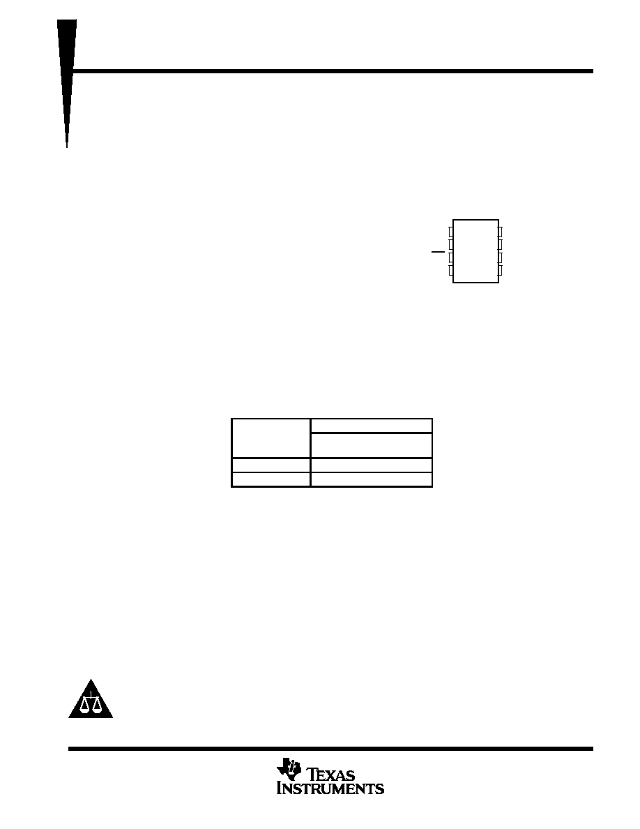
AVAILABLE OPTIONS
PACKAGE
TA
SOIC
(D)
0
∞
C to 70
∞
C
TLV5617ACD
≠ 40
∞
C to 85
∞
C
TLV5617AID
Please be aware that an important notice concerning availability, standard warranty, and use in critical applications of
Texas Instruments semiconductor products and disclaimers thereto appears at the end of this data sheet.
Copyright
©
2000, Texas Instruments Incorporated
PRODUCTION DATA information is current as of publication date.
Products conform to specifications per the terms of Texas Instruments
standard warranty. Production processing does not necessarily include
testing of all parameters.
1
2
3
4
8
7
6
5
DIN
SCLK
CS
OUTA
V
DD
OUTB
REF
AGND
D PACKAGE
(TOP VIEW)
SPI and QSPI are trademarks of Motorola, Inc.
Microwire is a trademark of National Semiconductor Corporation.
TLV5617A
2.7-V TO 5.5-V LOW-POWER DUAL 10-BIT DIGITAL-TO-ANALOG
CONVERTER WITH POWER DOWN
SLAS234B ≠ JULY 1999 ≠ REVISED MARCH 2000
2
POST OFFICE BOX 655303
∑
DALLAS, TEXAS 75265
functional block diagram
Serial
Interface
and
Control
10-Bit
DAC B
Latch
SCLK
DIN
CS
OUTA
Power-On
Reset
x2
10
Power and
Speed Control
2
10-Bit
DAC A
Latch
10
REF
AGND
VDD
10
10
OUTB
x2
Buffer
10
Terminal Functions
TERMINAL
I/O/P
DESCRIPTION
NAME
NO.
I/O/P
DESCRIPTION
AGND
5
P
Ground
CS
3
I
Chip select. Digital input active low, used to enable/disable inputs.
DIN
1
I
Digital serial data input
OUTA
4
O
DAC A analog voltage output
OUTB
7
O
DAC B analog voltage output
REF
6
I
Analog reference voltage input
SCLK
2
I
Digital serial clock input
VDD
8
P
Positive power supply
TLV5617A
2.7-V TO 5.5-V LOW-POWER DUAL 10-BIT DIGITAL-TO-ANALOG
CONVERTER WITH POWER DOWN
SLAS234B ≠ JULY 1999 ≠ REVISED MARCH 2000
3
POST OFFICE BOX 655303
∑
DALLAS, TEXAS 75265
absolute maximum ratings over operating free-air temperature range (unless otherwise noted)
Supply voltage (V
DD
to AGND)
7 V
. . . . . . . . . . . . . . . . . . . . . . . . . . . . . . . . . . . . . . . . . . . . . . . . . . . . . . . . . . . . . . .
Reference input voltage range
≠ 0.3 V to V
DD
+ 0.3 V
. . . . . . . . . . . . . . . . . . . . . . . . . . . . . . . . . . . . . . . . . . . . . . .
Digital input voltage range
≠ 0.3 V to V
DD
+ 0.3 V
. . . . . . . . . . . . . . . . . . . . . . . . . . . . . . . . . . . . . . . . . . . . . . . . . .
Operating free-air temperature range, T
A
: TLV5617AC 0
∞
C to 70
∞
C
. . . . . . . . . . . . . . . . . . . . . . . . . . . . . . . . . . .
TLV5617AI ≠ 40
∞
C to 85
∞
C
. . . . . . . . . . . . . . . . . . . . . . . . . . . . . . . . . .
Storage temperature range, T
stg
≠ 65
∞
C to 150
∞
C
. . . . . . . . . . . . . . . . . . . . . . . . . . . . . . . . . . . . . . . . . . . . . . . . . . .
Lead temperature 1,6 mm (1/16 inch) from case for 10 seconds
260
∞
C
. . . . . . . . . . . . . . . . . . . . . . . . . . . . . . .
Stresses beyond those listed under "absolute maximum ratings" may cause permanent damage to the device. These are stress ratings only, and
functional operation of the device at these or any other conditions beyond those indicated under "recommended operating conditions" is not
implied. Exposure to absolute-maximum-rated conditions for extended periods may affect device reliability.
recommended operating conditions
MIN
NOM
MAX
UNIT
Supply voltage VDD
VDD = 5 V
4.5
5
5.5
V
Supply voltage, VDD
VDD = 3 V
2.7
3
3.3
Power on reset, POR
0.55
2
V
High-level digital input voltage, VIH
VDD = 2.7 V to 5.5 V
2
V
Low-level digital input voltage, VIL
VDD = 2.7 V to 5.5 V
0.8
V
Reference voltage, Vref to REF terminal
VDD = 5 V (see Note 1)
AGND
2.048
VDD ≠1.5
V
Reference voltage, Vref to REF terminal
VDD = 3 V (see Note 1)
AGND
1.024
VDD ≠ 1.5
V
Load resistance, RL
2
k
Load capacitance, CL
100
pF
Clock frequency, fCLK
20
MHz
Operating free air temperature TA
TLV5617AC
0
70
∞
C
Operating free-air temperature, TA
TLV5617AI
≠40
85
∞
C
NOTE 1: Due to the x2 output buffer, a reference input voltage
(VDD≠0.4 V)/2 causes clipping of the transfer function.
TLV5617A
2.7-V TO 5.5-V LOW-POWER DUAL 10-BIT DIGITAL-TO-ANALOG
CONVERTER WITH POWER DOWN
SLAS234B ≠ JULY 1999 ≠ REVISED MARCH 2000
4
POST OFFICE BOX 655303
∑
DALLAS, TEXAS 75265
electrical characteristics over recommended operating conditions (unless otherwise noted)
power supply
PARAMETER
TEST CONDITIONS
MIN
TYP
MAX
UNIT
IDD
Power supply current
No load, All inputs = AGND or VDD,
Fast
1.7
2.5
mA
IDD
Power su
ly current
DD
DAC latch
0x800
mA
DD
y
DAC latch = 0x800
Slow
0.7
1
Slow
0.7
1
Power down supply current
1
µ
A
PSRR
Power supply rejection ratio
Zero scale, See Note 2
≠65
dB
PSRR
Power supply rejection ratio
Full scale, See Note 3
≠65
dB
NOTES:
2. Power supply rejection ratio at zero scale is measured by varying VDD and is given by:
PSRR = 20 log [(EZS(VDDmax) ≠ EZS(VDDmin)/VDDmax]
3. Power supply rejection ratio at full scale is measured by varying VDD and is given by:
PSRR = 20 log [(EG(VDDmax) ≠ EG(VDDmin)/VDDmax]
static DAC specifications
PARAMETER
TEST CONDITIONS
MIN
TYP
MAX
UNIT
Resolution
10
bits
INL
Integral nonlinearity
See Note 4
±
0.7
±
1
LSB
DNL
Differential nonlinearity
See Note 5
±
0.1
±
1
LSB
EZS
Zero-scale error (offset error at zero scale)
See Note 6
±
12
mV
EZS TC
Zero-scale-error temperature coefficient
See Note 7
10
ppm/
∞
C
EG
Gain error
See Note 8
±
0.6
% full
scale V
EG TC
Gain-error temperature coefficient
See Note 9
10
ppm/
∞
C
NOTES:
4. The relative accuracy of integral nonlinearity (INL), sometimes referred to as linearity error, is the maximum deviation of the output
from the line between zero and full scale, excluding the effects of zero-code and full-scale errors.
5. The differential nonlinearity (DNL), sometimes referred to as differential error, is the difference between the measured and ideal
1-LSB amplitude change of any two adjacent codes.
6. Zero-scale error is the deviation from zero voltage output when the digital input code is zero.
7. Zero-scale-error temperature coefficient is given by: EZS TC = [EZS (Tmax) ≠ EZS (Tmin)]/2Vref
◊
106/(Tmax ≠ Tmin).
8. Gain error is the deviation from the ideal output (2Vref ≠ 1 LSB) with an output load of 10 k
.
9. Gain temperature coefficient is given by: EG TC = [EG (Tmax) ≠ Eg (Tmin)]/2Vref
◊
106/(Tmax ≠ Tmin).
output specifications
PARAMETER
TEST CONDITIONS
MIN
TYP
MAX
UNIT
VO
Output voltage range
RL = 10 k
VDD≠0.4
V
Output load regulation accuracy
VO = 4.096 V, 2.048 V RL = 2 k
±
0.29
% FS
reference input
PARAMETER
TEST CONDITIONS
MIN
TYP
MAX
UNIT
VI
Input voltage range
0
VDD≠1.5
V
RI
Input resistance
10
M
CI
Input capacitance
5
pF
Reference input bandwidth
REF = 0 2 V
+ 1 024 V dc
Fast
1.3
MHz
Reference input bandwidth
REF = 0.2 Vpp + 1.024 V dc
Slow
525
kHz
Reference feedthrough
REF = 1 Vpp at 1 kHz + 1.024 V dc (see Note 10)
≠ 80
dB
NOTE 10: Reference feedthrough is measured at the DAC output with an input code = 0x000.

TLV5617A
2.7-V TO 5.5-V LOW-POWER DUAL 10-BIT DIGITAL-TO-ANALOG
CONVERTER WITH POWER DOWN
SLAS234B ≠ JULY 1999 ≠ REVISED MARCH 2000
5
POST OFFICE BOX 655303
∑
DALLAS, TEXAS 75265
electrical characteristics over recommended operating conditions (unless otherwise noted)
(Continued)
digital inputs
PARAMETER
TEST CONDITIONS
MIN
TYP
MAX
UNIT
IIH
High-level digital input current
VI = VDD
1
µ
A
IIL
Low-level digital input current
VI = 0 V
≠1
µ
A
Ci
Input capacitance
8
pF
analog output dynamic performance
PARAMETER
TEST CONDITIONS
MIN
TYP
MAX
UNIT
t (FS)
Output settling time full scale
RL = 10 k
,
CL = 100 pF,
Fast
2.5
µ
s
ts(FS)
Output settling time, full scale
L
,
L
,
See Note 11
Slow
12
µ
s
t (CC)
Output settling time code to code
RL = 10 k
,
CL = 100 pF,
Fast
1
µ
s
ts(CC)
Output settling time, code to code
L
,
L
,
See Note 12
Slow
2
µ
s
SR
Slew rate
RL = 10 k
,
CL = 100 pF,
Fast
3
V/
µ
s
SR
Slew rate
L
,
L
,
See Note 13
Slow
0.5
V/
µ
s
Glitch energy
DIN = 0 to 1,
FCLK = 100 kHz,
CS = VDD
5
nV≠s
SNR
Signal-to-noise ratio
56
SINAD
Signal-to-noise + distortion
fs = 102 kSPS, fout = 1 kHz,
55
dB
THD
Total harmonic distortion
s
,
out
,
RL = 10 k
,
CL = 100 pF
≠62
dB
SFDR
Spurious free dynamic range
64
NOTES: 11. Settling time is the time for the output signal to remain within
±
0.5 LSB of the final measured value for a digital input code change
of 0x020 to 0xFDC and 0xFDC to 0x020 respectively. Not tested, assured by design.
12. Settling time is the time for the output signal to remain within
±
0.5 LSB of the final measured value for a digital input code change
of one count. Not tested, assured by design.
13. Slew rate determines the time it takes for a change of the DAC output from 10% to 90% of full-scale voltage.