 | –≠–ª–µ–∫—Ç—Ä–æ–Ω–Ω—ã–π –∫–æ–º–ø–æ–Ω–µ–Ω—Ç: TLV5630 | –°–∫–∞—á–∞—Ç—å:  PDF PDF  ZIP ZIP |
www.ti.com
FEATURES
APPLICATIONS
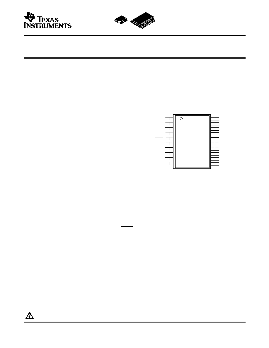
1
2
3
4
5
6
7
8
9
10
20
19
18
17
16
15
14
13
12
11
DGND
DIN
SCLK
FS
PRE
OUTE
OUTF
OUTG
OUTH
AGND
DV
DD
DOUT
LDAC
MODE
REF
OUTD
OUTC
OUTB
OUTA
AV
DD
DW OR PW PACKAGE
(TOP VIEW)
DESCRIPTION
TLV5630
TLV5631
TLV5632
SLAS269D ≠ MAY 2000 ≠ REVISED MARCH 2004
8-CHANNEL, 12-/10-/8-BIT, 2.7-V TO 5.5-V LOW POWER DIGITAL-TO-ANALOG
CONVERTERS WITH POWER DOWN AND INTERNAL REFERENCE
∑
Digital Servo Control Loops
∑
Eight Voltage Output DACs in One Package
∑
Digital Offset and Gain Adjustment
≠ TLV5630 . . . 12-Bit
∑
Industrial Process Control
≠ TLV5631 . . . 10-Bit
∑
Machine and Motion Control Devices
≠ TLV5632 . . . 8-Bit
∑
Mass Storage Devices
≠ 1 µs in Fast Mode
≠ 3 µs in Slow Mode
∑
Programmable Settling Time vs Power
Consumption
≠ 1 µs in Fast Mode
≠ 3 µs in Slow Mode
≠ 18 mW in Slow Mode at 3 V
≠ 48 mW in Fast Mode at 3 V
∑
Compatible With TMS320 and SPI Serial Ports
∑
Monotonic Over Temperature
∑
Low Power Consumption:
≠ 18 mW in Slow Mode at 3 V
≠ 48 mW in Fast Mode at 3 V
∑
Power-Down Mode
∑
Internal Reference
∑
Data Output for Daisy-Chaining
The TLV5630, TLV5631, and TLV5632 are pin-compatible, eight-channel, 12-/10-/8-bit voltage output DACs
each with a flexible serial interface. The serial interface allows glueless interface to TMS320 and SPI, QSPI, and
Microwire serial ports. It is programmed with a 16-bit serial string containing 4 control and 12 data bits.
Additional features are a power-down mode, an LDAC input for simultaneous update of all eight DAC outputs,
and a data output which can be used to cascade multiple devices, and an internal programmable band-gap
reference.
The resistor string output voltage is buffered by a rail-to-rail output amplifier with a programmable settling time to
allow the designer to optimize speed vs power dissipation. The buffered, high-impedance reference input can be
connected to the supply voltage.
Implemented with a CMOS process, the DACs are designed for single-supply operation from 2.7 V to 5.5 V. The
devices are available in 20-pin SOIC and TSSOP packages.
Please be aware that an important notice concerning availability, standard warranty, and use in critical applications of Texas
Instruments semiconductor products and disclaimers thereto appears at the end of this data sheet.
PRODUCTION DATA information is current as of publication date.
Copyright © 2000≠2004, Texas Instruments Incorporated
Products conform to specifications per the terms of the Texas
Instruments standard warranty. Production processing does not
necessarily include testing of all parameters.
www.ti.com
OUTA
12/10/8
12/10/8
Band-Gap
Voltage
2
Serial
Interface
12
8
REF
SCLK
DIN
FS
MODE
DOUT
DAC B, C, D, E, F, G and H
Same as DAC A
OUT
1 V or 2 V
PRE
LDAC
(Trimmed)
with Enable
X2
B, C, D,
E, F, G
and H
DAC A
Holding
Latch
DAC A
Latch
12/10/8
TLV5630
TLV5631
TLV5632
SLAS269D ≠ MAY 2000 ≠ REVISED MARCH 2004
These devices have limited built-in ESD protection. The leads should be shorted together or the device placed in conductive foam
during storage or handling to prevent electrostatic damage to the MOS gates.
AVAILABLE OPTIONS
PACKAGE
T
A
SOIC (DW)
TSSOP (PW)
RESOLUTION
TLV5630IDW
TLV5630IPW
12
40
∞
C to 85
∞
C
TLV5631IDW
TLV5631IPW
10
TLV5632IDW
TLV5632IPW
8
FUNCTIONAL BLOCK DIAGARAM
Terminal Functions
TERMINAL
I/O
DESCRIPTION
NAME
NO.
AGND
10
P
Analog ground
AV
DD
11
P
Analog power supply
DGND
1
P
Digital ground
DIN
2
I
Digital serial data input
DOUT
19
O
Digital serial data output
DV
DD
20
P
Digital power supply
FS
4
I
Frame sync input
LDAC
18
I
Load DAC. The DAC outputs are only updated, if this signal is low. It is an asynchronous input.
MODE
17
I
DSP/µC mode pin. High = µC mode, NC = DSP mode.
PRE
5
I
Preset input
REF
16
I/O
Voltage reference input/output
SCLK
3
I
Serial clock input
OUTA-OUTH
12-15, 6-9
O
DAC outputs A, B, C, D, E, F, G and H
2

www.ti.com
ABSOLUTE MAXIMUM RATINGS
RECOMMENDED OPERATING CONDITIONS
TLV5630
TLV5631
TLV5632
SLAS269D ≠ MAY 2000 ≠ REVISED MARCH 2004
over operating free-air temperature (unless otherwise noted)
(1)
UNIT
Supply voltage, (AV
DD
, DV
DD
to GND)
7 V
Reference input voltage range
- 0.3 V to AV
DD
+ 0.3
Digital input voltage range
- 0.3 V to DV
DD
+ 0.3
Operating free-air temperature range, T
A
-40
∞
C to 85
∞
C
Storage temperature range, T
stg
-65
∞
C to 150
∞
C
Lead temperature 1,6 mm (1/16 inch) from case for 10 seconds
260
∞
C
(1)
Stresses beyond those listed under,, absolute maximum ratings" may cause permanent damage to the device. These are stress ratings
only, and functional operation of the device at these or any other conditions beyond those indicated under,, recommended operating
conditions" is not implied. Exposure to absolute-maximum-rated conditions for extended periods may affect device reliability.
MIN
TYP
MAX
UNIT
5-V operation
4.5
5
5.5
V
Supply voltage, AV
DD
, DV
DD
3-V operation
2.7
3
3.3
V
DV
DD
= 2.7 V
2
High-level digital input, V
IH
V
DV
DD
= 5.5 V
2.4
DV
DD
= 2.7 V
0.6
Low-level digital input, V
IL
V
DV
DD
= 5.5 V
1.0
AV
DD
= 5 V
GND
2.048
AV
DD
Reference voltage, V
ref
V
AV
DD
= 3 V
GND
1.024
AV
DD
Analog output load resistance, R
L
2
k
Analog output load capacitance, C
L
100
pF
Clock frequency, f
CLK
30
MHz
Operating free-air temperature, T
A
-40
85
∞
C
3

www.ti.com
ELECTRICAL CHARACTERISTICS
TLV5630
TLV5631
TLV5632
SLAS269D ≠ MAY 2000 ≠ REVISED MARCH 2004
over recommended operating conditions (unless otherwise noted)
PARAMETER
TEST CONDITIONS
MIN
TYP
MAX
UNIT
POWER SUPPLY
Fast
16
21
No load, All inputs = DV
DD
or GND,
I
DD
Power supply current
mA
V
ref
= 2.048 V,
Slow
6
8
Power-down supply
0.1
µA
current
POR
Power on threshold
2
V
Power supply rejection
PSRR
Full scale, See
(1)
50
dB
ratio
STATIC DAC SPECIFICATIONS
TLV5630
12
Bits
Resolution
TLV5631
10
Bits
TLV5632
8
Bits
TLV5630
Code 40 to 4095
±
2
±
6
LSB
INL
Integral nonlinearity
TLV5631
V
ref
= 1 V, 2 V
Code 20 to 1023
±
0.5
±
2
LSB
TLV5632
Code 6 to 255
±
0.3
±
1
LSB
TLV5630
Code 40 to 4095
±
0.5
±
1
LSB
DNL
Differential nonlinearity
TLV5631
V
ref
= 1 V, 2 V
Code 20 to 1023
±
0.1
±
1
LSB
TLV5632
Code 6 to 255
±
0.1
±
1
LSB
Zero scale error (offset error at zero
E
ZS
±
30
mV
scale)
Zero scale error temperature coef-
E
ZS
TC
30
µV/
∞
C
ficient
%Full
E
G
Gain error
±
0.6
Scale V
EGTC
Gain error temperature coefficient
10
ppm/
∞
C
OUTPUT SPECIFICATIONS
V
O
Voltage output range
R
L
= 10 k
0
AV
DD
-0.4
V
Output load regulation
%Full
R
L
= 2 k
vs 10 k
±
0.3
accuracy
Scale V
REFERENCE OUTPUT
V
REFOU
Low reference voltage
V
DD
> 4.75 V
1.010
1.024
1.040
V
TL
V
REFOU
High reference voltage
2.020
2.048
2.096
V
TH
I
ref(Sourc
Output source current
1
mA
e)
I
ref(Sink)
Output sink current
-1
mA
Load capacitance
See
(2)
1
10
µF
Power supply rejection
PSRR
60
dB
ratio
REFERENCE INPUT
V
I
Input voltage range
0
AV
DD
V
R
I
Input resistance
50
k
C
i
Input capacitance
10
pF
Fast
2.2
MHz
Reference input
V
ref
= 0.4 V
pp
+ 2.048 Vdc,
bandwidth
Input code = 0x800
Slow
1.9
MHz
(1)
Power supply rejection ratio at full scale is measured by varying AV
DD
and is given by: PSRR = 20 log [(E
G
(AV
DD
max) -
E
G
(AV
DD
min))/V
DD
max]
(2)
In parallel with a 100-nF capacitor
4
www.ti.com
DIGITAL INPUT TIMING REQUIREMENTS
TLV5630
TLV5631
TLV5632
SLAS269D ≠ MAY 2000 ≠ REVISED MARCH 2004
ELECTRICAL CHARACTERISTICS (continued)
over recommended operating conditions (unless otherwise noted)
PARAMETER
TEST CONDITIONS
MIN
TYP
MAX
UNIT
Reference feedthrough
V
ref
= 2 V
pp
at 1 kHz + 2.048 Vdc, See
(3)
84
dB
DIGITAL INPUTS
I
IH
High-level digital input
V
I
= DV
DD
1
µA
current
I
IL
Low-level digital input
V
I
= 0 V
1
µA
current
C
I
Input capacitance
8
pF
DIGITAL OUTPUT
V
OH
High-level digital output R
L
= 10 k
2.6
V
voltage
V
OL
Low-level digital output
R
L
= 10 k
0.4
V
voltage
Output voltage rise
R
L
= 10 k
, C
L
= 20 pF, Includes propagation delay
5
10
ns
time
ANALOG OUTPUT DYNAMIC PERFORMANCE
Fast
1
3
Output settling time, full
t
s(FS)
R
L
= 10 k
, C
L
= 100 pF, See
(4)
µs
scale
Slow
3
7
Fast
0.5
1
Output settling time,
t
s(CC)
R
L
= 10 k
, C
L
= 100 pF, See
(5)
µs
code to code
Slow
1
2
Fast
4
10
SR
Slew rate
R
L
= 10 k
, C
L
= 100 pF, See
(6)
V/µs
Slow
1
3
Glitch energy
See
(7)
4
nV-s
Channel crosstalk
10 kHz sine, 4 V
PP
90
dB
(3)
Reference feedthrough is measured at the DAC output with an input code = 0x000.
(4)
Settling time is the time for the output signal to remain within
±
0.5 LSB of the final measured value for a digital input code change of
0x080 to 0xFFF and 0xFFF to 0x080, respectively. Assured by design; not tested.
(5)
Settling time is the time for the output signal to remain within
±
0.5 LSB of the final measured value for a digital input code change of one
count. The max time applies to code changes near zero scale or full scale. Assured by design; not tested.
(6)
Slew rate determines the time it takes for a change of the DAC output from 10% to 90% full-scale voltage.
(7)
Code transition: TLV5630 - 0x7FF to 0x800, TLV5631 - 0x7FCto 0x800, TLV5632 - 0x7F0 to 0x800.
PARAMETER
MIN
TYP
MAX
UNIT
t
su(FS-CK)
Setup time, FS low before next negative SCLK edge
8
ns
Setup time, 16
th
negative edge after FS low on which bit D0 is sampled before rising edge
t
su(C16-FS)
10
ns
of FS. µC mode only
t
su(FS-C17)
µC mode, setup time, FS high before 17
th
positive SCLK.
10
ns
t
su(CK-FS)
DSP mode, setup time, SLCK low before FS low.
5
ns
t
wL(LDAC)
LDAC duration low
10
ns
t
su(FS-CK)
Setup time, FS low before first negative SCLK edge
8
ns
t
wL
SCLK pulse duration low
16
t
su(D)
Setup time, data ready before SCLK falling edge
8
ns
t
h(D)
Hold time, data held valid after SCLK falling edge
5
ns
t
wH(FS)
FS duration high
10
ns
t
wL(FS)
FS duration low
10
ns
See AC
t
s
Settling time
specs
5