Document Outline
- features
- applications
- description
- ORDERING INFORMATION
- functional block diagram
- Terminal Functions
- absolute maximum ratings over operating free-air temperature range (unl\
ess otherwise noted)
- recommended operating conditions
- electrical characteristics over recommended operating conditions, V ref \
= 2.048 V, V ref = 1.024 V
(unless otherwise noted)
- power supply
- static DAC specifications
- output specifications
- reference pin configured as output (REF)
- reference pin configured as input (REF)
- digital inputs
- electrical characteristics over recommended operating conditions (unles\
s otherwise noted)
- analog output dynamic performance
- digital input timing requirements
- PARAMETER MEASUREMENT INFORMATION
- TYPICAL CHARACTERISTICS
- APPLICATION INFORMATION
- general function
- serial interface
- serial clock frequency and update rate
- data format
- register select bits
- data bits: DAC A, DAC B and BUFFER
- data bits: CONTROL
- reference bits
- Examples of operation:
- linearity, offset, and gain error using single ended supplies
- definitions of specifications and terminology
- integral nonlinearity (INL)
- differential nonlinearity (DNL)
- zero-scale error (E ZS)
- gain error (E G)
- total harmonic distortion (THD)
- signal-to-noise ratio + distortion (S/N+D)
- spurious free dynamic range (SFDR)
TLV5638-EP
2.7-V TO 5.5-V LOW-POWER DUAL 12-BIT DIGITAL-TO-ANALOG
CONVERTER WITH INTERNAL REFERENCE AND POWER DOWN
SGLS130A ≠ JULY 2002 ≠ REVISED JULY 2003
1
POST OFFICE BOX 655303
∑
DALLAS, TEXAS 75265
features
D
Controlled Baseline
≠ One Assembly/Test Site, One Fabrication
Site
D
Extended Temperature Performance up to
≠55
∞
C to 125
∞
C
D
Enhanced Diminishing Manufacturing
Sources (DMS) Support
D
Enhanced Product Change Notification
D
Qualification Pedigree
D
Dual 12-Bit Voltage Output DAC
D
Programmable Internal Reference
D
Programmable Settling Time:
1
µ
s in Fast Mode,
3.5
µ
s in Slow Mode
Component qualification in accordance with JEDEC and industry
standards to ensure reliable operation over an extended
temperature range. This includes, but is not limited to, Highly
Accelerated Stress Test (HAST) or biased 85/85, temperature
cycle, autoclave or unbiased HAST, electromigration, bond
intermetallic life, and mold compound life. Such qualification
testing should not be viewed as justifying use of this component
beyond specified performance and environmental limits.
D
Compatible With TMS320 and SPI
Serial
Ports
D
Differential Nonlinearity <0.5 LSB Typ
D
Monotonic Over Temperature
applications
D
Digital Servo Control Loops
D
Digital Offset and Gain Adjustment
D
Industrial Process Control
D
Machine and Motion Control Devices
D
Mass Storage Devices
description
The TLV5638 is a dual 12-bit voltage output DAC with a flexible 3-wire serial interface. The serial interface allows
glueless interface to TMS320 and SPI
, QSPI
, and Microwire
serial ports. It is programmed with a 16-bit
serial string containing 4 control and 12 data bits.
The resistor string output voltage is buffered by a x2 gain rail-to-rail output buffer. The buffer features a Class
AB output stage to improve stability and reduce settling time. The programmable settling time of the DAC allows
the designer to optimize speed vs power dissipation. With its on-chip programmable precision voltage
reference, the TLV5638 simplifies overall system design.
Because of its ability to source up to 1 mA, the reference can also be used as a system reference. Implemented
with a CMOS process, the device is designed for single supply operation from 2.7 V to 5.5 V. It is available in
an 8-pin SOIC package to reduce board space.
ORDERING INFORMATION
TA
PACKAGE
ORDERABLE
PART NUMBER
TOP-SIDE
MARKING
≠40
∞
C to 125
∞
C
SOIC ≠ D
Tape and reel
TLV5638QDREP
5638QE
≠55
∞
C to 125
∞
C
SOIC ≠ D
Tape and reel
TLV5638MDREP
5638ME
Package drawings, standard packing quantities, thermal data, symbolization, and PCB design guidelines
are available at www.ti.com/sc/package.
Please be aware that an important notice concerning availability, standard warranty, and use in critical applications of
Texas Instruments semiconductor products and disclaimers thereto appears at the end of this data sheet.
Copyright
2002 ≠ 2003, Texas Instruments Incorporated
PRODUCTION DATA information is current as of publication date.
Products conform to specifications per the terms of Texas Instruments
standard warranty. Production processing does not necessarily include
testing of all parameters.
SPI and QSPI are trademarks of Motorola, Inc.
Microwire is a trademark of National Semiconductor Corporation.
1
2
3
4
8
7
6
5
DIN
SCLK
CS
OUTA
V
DD
OUTB
REF
AGND
D PACKAGE
(TOP VIEW)
TLV5638-EP
2.7-V TO 5.5-V LOW-POWER DUAL 12-BIT DIGITAL-TO-ANALOG
CONVERTER WITH INTERNAL REFERENCE AND POWER DOWN
SGLS130A ≠ JULY 2002 ≠ REVISED JULY 2003
2
POST OFFICE BOX 655303
∑
DALLAS, TEXAS 75265
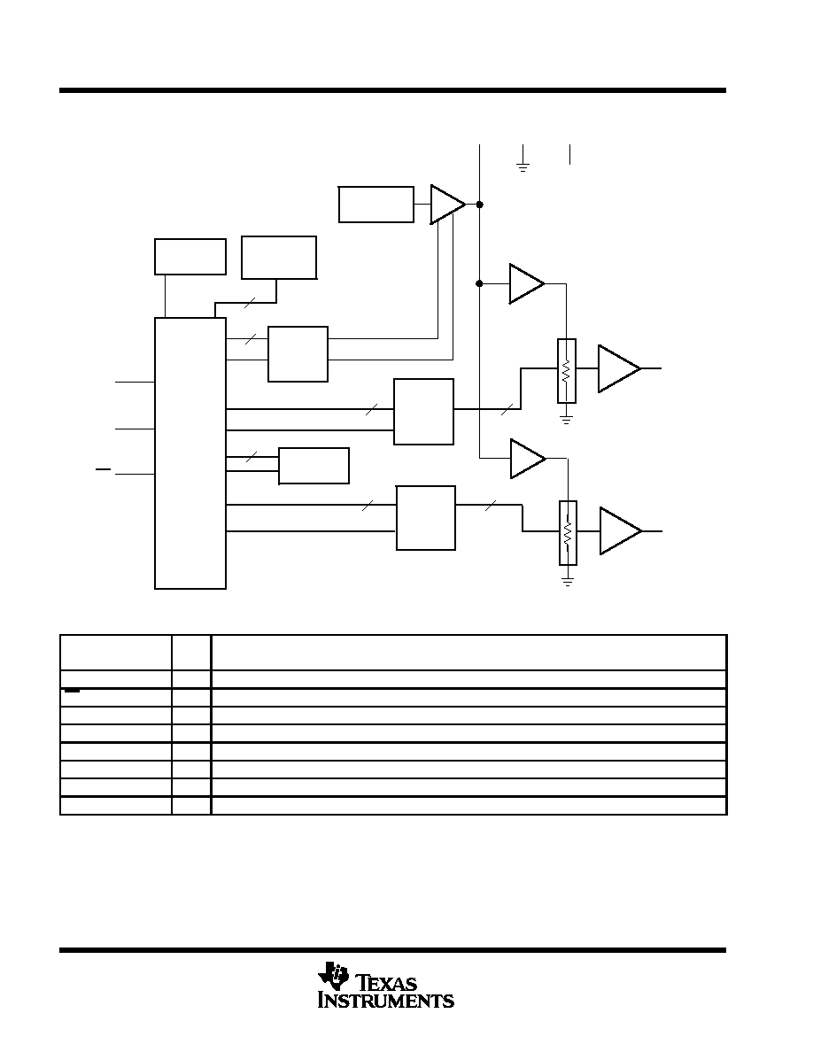
functional block diagram
Serial
Interface
and
Control
12-Bit
DAC B
Latch
SCLK
DIN
CS
OUTA
Power-On
Reset
x2
12
2-Bit
Control
Latch
Power
and Speed
Control
2
Voltage
Bandgap
PGA With
Output Enable
12-Bit
DAC A
Latch
12
REF
AGND
VDD
2
12
12
OUTB
x2
Buffer
12
Terminal Functions
TERMINAL
I/O/P
DESCRIPTION
NAME
NO.
I/O/P
DESCRIPTION
AGND
5
P
Ground
CS
3
I
Chip select. Digital input active low, used to enable/disable inputs
DIN
1
I
Digital serial data input
OUT A
4
O
DAC A analog voltage output
OUT B
7
O
DAC B analog voltage output
REF
6
I/O
Analog reference voltage input/output
SCLK
2
I
Digital serial clock input
VDD
8
P
Positive power supply
TLV5638-EP
2.7-V TO 5.5-V LOW-POWER DUAL 12-BIT DIGITAL-TO-ANALOG
CONVERTER WITH INTERNAL REFERENCE AND POWER DOWN
SGLS130A ≠ JULY 2002 ≠ REVISED JULY 2003
3
POST OFFICE BOX 655303
∑
DALLAS, TEXAS 75265
absolute maximum ratings over operating free-air temperature range (unless otherwise noted)
Supply voltage (V
DD
to AGND)
7 V
. . . . . . . . . . . . . . . . . . . . . . . . . . . . . . . . . . . . . . . . . . . . . . . . . . . . . . . . . . . . . . .
Reference input voltage range
≠0.3 V to V
DD
+ 0.3 V
. . . . . . . . . . . . . . . . . . . . . . . . . . . . . . . . . . . . . . . . . . . . . . . .
Digital input voltage range
≠0.3 V to V
DD
+ 0.3 V
. . . . . . . . . . . . . . . . . . . . . . . . . . . . . . . . . . . . . . . . . . . . . . . . . . .
Operating free-air temperature range, T
A
: TLV5638Q (see Note 1)
≠40
∞
C to 125
∞
C
. . . . . . . . . . . . . . . . . . . . .
TLV5638M (see Note 1)
≠55
∞
C to 125
∞
C
. . . . . . . . . . . . . . . . . . . . .
Storage temperature range, T
stg
(see Note 1)
≠65
∞
C to 150
∞
C
. . . . . . . . . . . . . . . . . . . . . . . . . . . . . . . . . . . . . . .
Package thermal impedance,
JA
: D package
131
∞
C/W
. . . . . . . . . . . . . . . . . . . . . . . . . . . . . . . . . . . . . . . . . . . .
Lead temperature 1,6 mm (1/16 inch) from case for 10 seconds
260
∞
C
. . . . . . . . . . . . . . . . . . . . . . . . . . . . . . .
Stresses beyond those listed under "absolute maximum ratings" may cause permanent damage to the device. These are stress ratings only, and
functional operation of the device at these or any other conditions beyond those indicated under "recommended operating conditions" is not
implied. Exposure to absolute-maximum-rated conditions for extended periods may affect device reliability.
NOTE 1: Long term high-temperature storage and/or extended use at maximum recommended operating conditions may result in a reduction
of overall device life. See www.ti.com/ep_quality for additional information on enhanced plastic packaging.
recommended operating conditions
MIN
NOM
MAX
UNIT
Supply voltage VDD
VDD = 5 V
4.5
5
5.5
V
Supply voltage, VDD
VDD = 3 V
2.7
3
3.3
V
Power on reset, POR
0.55
2
V
High-level digital input voltage, VIH
VDD = 2.7 V to 5.5 V
2
V
Low-level digital input voltage, VIL
VDD = 2.7 V to 5.5 V
0.8
V
Reference voltage, Vref to REF terminal
VDD = 5 V (see Note 1)
AGND
2.048
VDD ≠1.5
V
Reference voltage, Vref to REF terminal
VDD = 3 V (see Note 1)
AGND
1.024
VDD ≠ 1.5
V
Load resistance, RL
2
k
Load capacitance, CL
100
pF
Clock frequency, fCLK
20
MHz
Operating free air temperature TA
TLV5638Q (see Note 2)
≠40
125
∞
C
Operating free-air temperature, TA
TLV5638M (see Note 2)
≠55
125
∞
C
NOTES:
1. Due to the x2 output buffer, a reference input voltage
(VDD≠0.4 V)/2 causes clipping of the transfer function. The output buffer of
the internal reference must be disabled, if an external reference is used.
2. Long term high-temperature storage and/or extended use at maximum recommended operating conditions may result in a reduction
of overall device life. See www.ti.com/ep_quality for additional information on enhanced plastic packaging.

TLV5638-EP
2.7-V TO 5.5-V LOW-POWER DUAL 12-BIT DIGITAL-TO-ANALOG
CONVERTER WITH INTERNAL REFERENCE AND POWER DOWN
SGLS130A ≠ JULY 2002 ≠ REVISED JULY 2003
4
POST OFFICE BOX 655303
∑
DALLAS, TEXAS 75265
electrical characteristics over recommended operating conditions, V
ref
= 2.048 V, V
ref
= 1.024 V
(unless otherwise noted)
power supply
PARAMETER
TEST CONDITIONS
MIN
TYP
MAX
UNIT
VDD = 5 V,
Fast
4.3
7
mA
DD
Int. ref.
Slow
2.2
3.6
mA
No load
VDD = 3 V,
Fast
3.8
6.3
mA
IDD
Power supply current
No load,
All inputs = AGND
DD
Int. ref.
Slow
1.8
3.0
mA
IDD
Power supply current
or VDD,
DAC latch
0x800
VDD = 5 V,
Fast
3.9
6.3
mA
DAC latch = 0x800
DD
Ext. ref.
Slow
1.8
3.0
mA
VDD = 3 V,
Fast
3.5
5.7
mA
DD
Ext. ref.
Slow
1.5
2.6
mA
Power-down supply current
0.01
10
µ
A
PSRR
Power supply rejection ratio
Zero scale, See Note 2
≠65
dB
PSRR
Power supply rejection ratio
Full scale, See Note 3
≠65
dB
NOTES:
3. Power supply rejection ratio at zero scale is measured by varying VDD and is given by:
PSRR = 20 log [(EZS(VDDmax) ≠ EZS(VDDmin))/VDDmax]
4. Power supply rejection ratio at full scale is measured by varying VDD and is given by:
PSRR = 20 log [(EG(VDDmax) ≠ EG(VDDmin))/VDDmax]
static DAC specifications
PARAMETER
TEST CONDITIONS
MIN
TYP
MAX
UNIT
Resolution
12
bits
INL
Integral nonlinearity, end point adjusted
See Note 4
±
1.7
±
6
LSB
DNL
Differential nonlinearity
See Note 5
±
0.4
±
1
LSB
EZS
Zero-scale error (offset error at zero scale)
See Note 6
±
24
mV
EZS TC
Zero-scale-error temperature coefficient
See Note 7
10
ppm/
∞
C
EG
Gain error
See Note 8
±
0.6
% full
scale V
EG TC
Gain error temperature coefficient
See Note 9
10
ppm/
∞
C
NOTES:
5. The relative accuracy or integral nonlinearity (INL) sometimes referred to as linearity error, is the maximum deviation of the output
from the line between zero and full scale excluding the effects of zero code and full-scale errors. Tested from code 32 to 4095.
6. The differential nonlinearity (DNL) sometimes referred to as differential error, is the difference between the measured and ideal 1
LSB amplitude change of any two adjacent codes. Monotonic means the output voltage changes in the same direction (or remains
constant) as a change in the digital input code.
7. Zero-scale error is the deviation from zero voltage output when the digital input code is zero.
8. Zero-scale-error temperature coefficient is given by: EZS TC = [EZS (Tmax) ≠ EZS (Tmin)]/Vref
◊
106/(Tmax ≠ Tmin).
9. Gain error is the deviation from the ideal output (2Vref ≠ 1 LSB) with an output load of 10 k
excluding the effects of the zero-error.
10. Gain temperature coefficient is given by: EG TC = [EG(Tmax) ≠ EG (Tmin)]/Vref
◊
106/(Tmax ≠ Tmin).
TLV5638-EP
2.7-V TO 5.5-V LOW-POWER DUAL 12-BIT DIGITAL-TO-ANALOG
CONVERTER WITH INTERNAL REFERENCE AND POWER DOWN
SGLS130A ≠ JULY 2002 ≠ REVISED JULY 2003
5
POST OFFICE BOX 655303
∑
DALLAS, TEXAS 75265
electrical characteristics over recommended operating conditions, V
ref
= 2.048 V, V
ref
= 1.024 V
(unless otherwise noted) (continued)
output specifications
PARAMETER
TEST CONDITIONS
MIN
TYP
MAX
UNIT
VO
Output voltage
RL = 10 k
0
VDD≠0.4
V
Output load regulation accuracy
VO = 4.096 V, 2.048 V,
RL = 2 k
±
0.25
% full
scale V
reference pin configured as output (REF)
PARAMETER
TEST CONDITIONS
MIN
TYP
MAX
UNIT
Vref(OUTL)
Low reference voltage
1.003
1.024
1.045
V
Vref(OUTH)
High reference voltage
VDD > 4.75 V
2.027
2.048
2.069
V
Iref(source)
Output source current
1
mA
Iref(sink)
Output sink current
≠1
mA
Load capacitance
100
pF
PSRR
Power supply rejection ratio
≠65
dB
reference pin configured as input (REF)
PARAMETER
TEST CONDITIONS
MIN
TYP
MAX
UNIT
VI
Input voltage
0
VDD≠1.5
V
RI
Input resistance
10
M
CI
Input capacitance
5
pF
Reference input bandwidth
REF = 0 2 V
+ 1 024 V dc
Fast
1.3
MHz
Reference input bandwidth
REF = 0.2 Vpp + 1.024 V dc
Slow
525
kHz
Reference feedthrough
REF = 1 Vpp at 1 kHz + 1.024 V dc (see Note 10)
≠ 80
dB
NOTE 11: Reference feedthrough is measured at the DAC output with an input code = 0x000.
digital inputs
PARAMETER
TEST CONDITIONS
MIN
TYP
MAX
UNIT
IIH
High-level digital input current
VI = VDD
1
µ
A
IIL
Low-level digital input current
VI = 0 V
≠1
µ
A
Ci
Input capacitance
8
pF