 | –≠–ª–µ–∫—Ç—Ä–æ–Ω–Ω—ã–π –∫–æ–º–ø–æ–Ω–µ–Ω—Ç: TLV990 | –°–∫–∞—á–∞—Ç—å:  PDF PDF  ZIP ZIP |

TLV990
3-V, 10-BIT, 28-MSPS AREA CCD AND VIDEO SIGNAL PROCESSOR
SLVS298 ≠ MAY 2000
1
POST OFFICE BOX 655303
∑
DALLAS, TEXAS 75265
features
D
Single-Chip CCD and Video Signal
Processor
D
10-Bit, 28-MSPS, A/D-Converter Single 3-V
Supply Operation
D
Very Low Power: 150 mW Typical, 2-mW
Power-Down Mode
D
Differential Nonlinearity Error:
<
±
0.5 LSB Typical
D
Integral Nonlinearity Error: <
±
0.9 LSB
Typical
D
Programmable Gain Amplifier (PGA) With
0-dB to 36-dB Gain Range (0.045 dB/Step)
D
Automatic or Programmable Optical Black
Level and Offset Calibration With Digital
Filter and Bad Pixel Limits
D
Additional DACs for External Analog
Setting
D
Serial Interface for Register Configuration
D
Internal-Reference Voltages
D
48-Pin TQFP Package
application
D
Video Camcorder
description
The TLV990 is a complete CCD and video signal
processor/digitizer designed for video camcorder
applications. The TLV990 performs all the analog-processing functions necessary to maximize the dynamic
range, corrects various errors associated with the CCD sensor, and then digitizes the results with an on-chip
high-speed analog-to-digital converter (ADC).
The key components of the TLV990 include: an input clamp circuit for CCD and analog video signals, a
correlated double sampler (CDS), a programmable-gain amplifier (PGA) with 0 to 36-dB gain range, two internal
digital-to-analog converters (DAC) for automatic or programmable optical black level and offset calibration, a
10-bit, 28-MSPS pipeline ADC, a parallel data port for easy microprocessor interface, a serial port for
configuring internal control registers, two additional DACs for external system control, and internal reference
voltages.
Designed in advanced CMOS process, the TLV990 operates from a single 3-V power supply with a normal
power consumption of 150 mW at 28 MSPS, and 2 mW in power-down mode.
Its very high throughput rate, single 3-V operation, very low-power consumption, and fully-integrated analog
processing circuitry make the TLV990 an ideal CCD and video signal-processing solution for electronic
video-camcorder applications.
This device is available in a 48-pin TQFP package and is specified over a ≠20
∞
C to 75
∞
C operating-temperature
range.
Copyright
©
2000, Texas Instruments Incorporated
PRODUCTION DATA information is current as of publication date.
Products conform to specifications per the terms of Texas Instruments
standard warranty. Production processing does not necessarily include
testing of all parameters.
Please be aware that an important notice concerning availability, standard warranty, and use in critical applications of
Texas Instruments semiconductor products and disclaimers thereto appears at the end of this data sheet.
2
3
OE
SCKP
DACO2
DACO1
AGND3
AV
DD3
DIGND
DIV
DD
D9
D8
D7
D6
24
23
22
21
20
19
18
17
16
15
14
13
4
37
38
39
40
41
42
43
44
45
46
47
48
AGND5
RBD
RMD
RPD
AV
DD5
V
SS
AV
DD1
AGND1
SR
SV
CLCCD
CLREF
5
6
7
8
RESET
CS
SDIN
SCLK
35 34 33 32 31
36
30
BLKG
CL
VDO
ADDOS
AV
AGND4
D3
D4
D5
DD2
D0
D1
D2
28 27 26
29
9 10 11 12
25
1
ADCCLK
OBCLP
STBY
VIDEOIN
CCDIN
AGND2
PFB PACKAGE
(TOP VIEW)
AV
DGND
DD
DV
DD4
TLV990PFB

TLV990
3-V, 10-BIT, 28-MSPS AREA CCD AND VIDEO SIGNAL PROCESSOR
SLVS298 ≠ MAY 2000
2
POST OFFICE BOX 655303
∑
DALLAS, TEXAS 75265
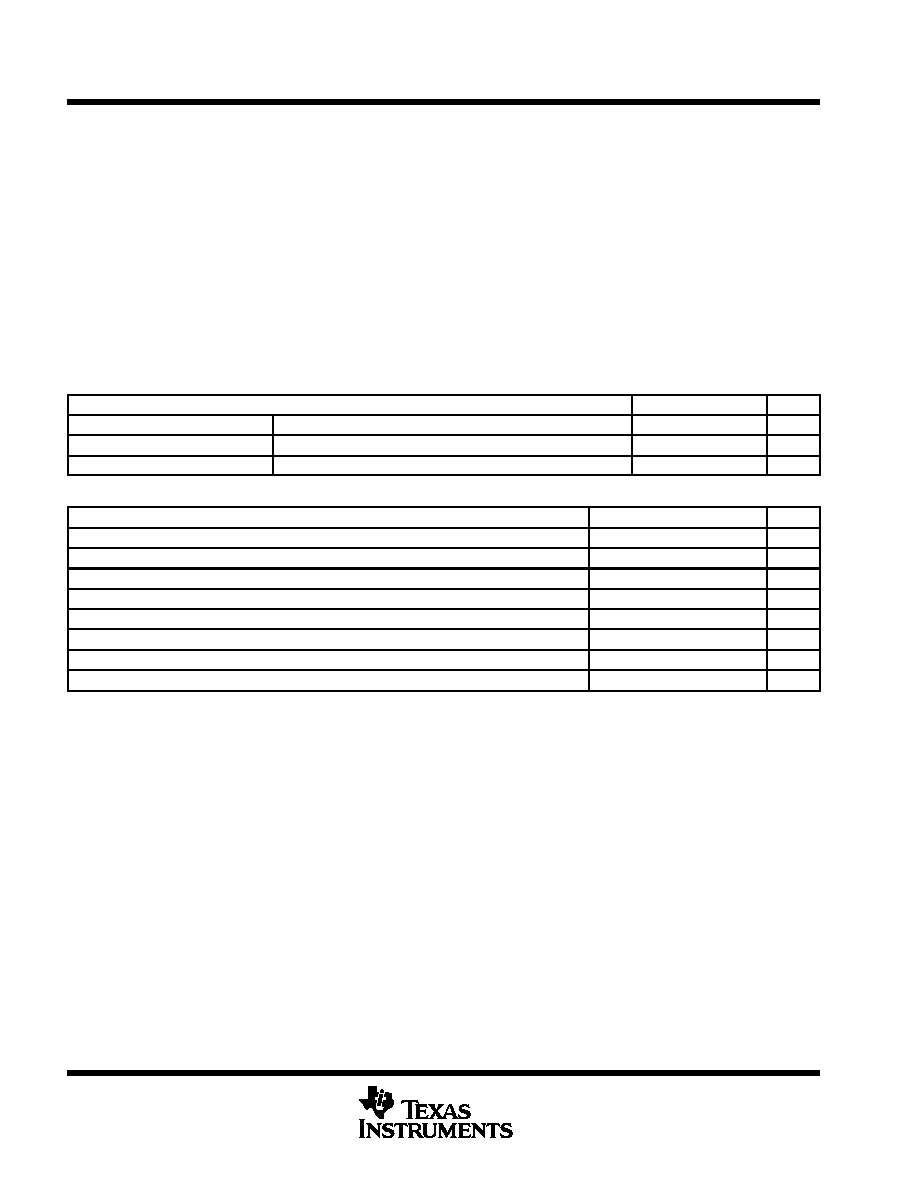
AVAILABLE OPTIONS
PACKAGE DEVICE
TA
TQFP
(PFB)
≠ 20
∞
C to 75
∞
C
TLV990PFB
functional block diagram
10-Bit
ADC
PGA
8-Bit
ADC
Offset
Register
PGA
Regulator
10
8-Bit
ADC
Offset
Register
INT. REF.
Optical
Black
Pixel Limits
Digital
Averager/
Filter
Three
State
Latch
Timing
and
Control
Logic
Serial
Port
DAC
REG
8-Bit
DAC
DAC
REG
10-Bit
ADC
Clamp
1.2 V REF
CCDIN
VIDEOIN
DACO1
DACO2
CLCCD CLREF
AVDD1≠5
RPD
RBD
RMD
OE
D0
D9
RESET
CLK
SV
SR
BLKG
OBCLP
STBY
CS
SCLK
SDIN
DIGND
DGND
AGND1≠5
VSS
ADDOS
SCKP
CDS/
MUX
DVDD DIVDD
CLVDO

TLV990
3-V, 10-BIT, 28-MSPS AREA CCD AND VIDEO SIGNAL PROCESSOR
SLVS298 ≠ MAY 2000
3
POST OFFICE BOX 655303
∑
DALLAS, TEXAS 75265
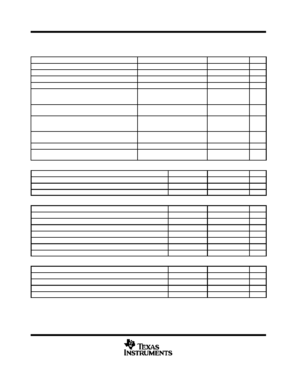
Terminal Functions
TERMINAL
I/O
DESCRIPTION
NAME
NO.
ADCCLK
25
I
ADC clock input
ADDOS
34
I
A dc offset is added to video input signal when the ADDOS is pulled low.
AGND1
44
Analog ground for internal CDS circuits
AGND2
4
Analog ground for internal PGA circuits
AGND3
20
Analog ground for internal DAC circuits
AGND4
32
Analog ground for internal ADC circuits
AGND5
37
Analog ground for internal REF circuits
AVDD1
43
Analog supply voltage for internal CDS circuits, 3 V
AVDD2
3
Analog supply voltage for internal PGA circuits, 3 V
AVDD3
19
Analog supply voltage for internal DAC circuits, 3 V
AVDD4
33
Analog supply voltage for internal ADC circuits, 3 V
AVDD5
41
Analog supply voltage for internal ADC circuits, 3 V
BLKG
36
I
Control input. The CDS operation is disabled when the BLKG is pulled low.
CLCCD
47
I
CCD signal clamp control input
CCDIN
1
I
CCD input
CLREF
48
O
Clamp reference voltage output
CLVDO
35
I
Video-signal clamp-control input. Only used in manual clamping mode. Active low.
CS
28
I
Chip select. A logic low on this input enables the serial port.
D0 ≠ D9
7≠16
O
10-bit 3-state ADC output data or offset DACs test data
DACO1
21
O
Digital-to-analog converter output1
DACO2
22
O
Digital-to-analog converter output2
DGND
5
Digital ground
DIGND
18
Digital interface circuit ground
DIVDD
17
Digital interface circuit supply voltage, 1.8 V≠ 4.4 V
DVDD
6
Digital supply voltage, 3 V
OBCLP
31
I
Optical black level and offset calibration control input. Active low.
OE
24
I
Output data enable. Active low.
RBD
38
O
Internal bandgap reference for external decoupling
RESET
29
I
Hardware-reset input, active low. This signal forces a reset of all internal registers
RMD
39
O
Ref≠ output for external decoupling
RPD
40
O
Ref+ output for external decoupling
SDIN
27
I
Serial data input to configure the internal registers
SCKP
23
I
Selects the polarity of SCLK. 0 ≠ active low (high when SCLK is not running), 1 ≠ active high (low when
SCLK is not running)
SCLK
26
I
Serial clock input. This clock synchronizes the serial data transfer.
SR
45
I
CCD reference level sample clock input
STBY
30
I
Hardware power-down control input, active low
SV
46
I
CCD signal level sample clock input
VIDEOIN
2
I
Analog video signal input
VSS
42
Silicon substrate, normally connected to analog ground
TLV990
3-V, 10-BIT, 28-MSPS AREA CCD AND VIDEO SIGNAL PROCESSOR
SLVS298 ≠ MAY 2000
4
POST OFFICE BOX 655303
∑
DALLAS, TEXAS 75265
absolute maximum ratings over operating free-air temperature (unless otherwise noted)
Supply voltage, AV
DD
, DV
DD
, DIV
DD
≠0.3 V to 6.5 V
. . . . . . . . . . . . . . . . . . . . . . . . . . . . . . . . . . . . . . . . . . . . . . . .
Analog input voltage range
≠0.3 V to AV
DD
+0.3 V
. . . . . . . . . . . . . . . . . . . . . . . . . . . . . . . . . . . . . . . . . . . . . . . . . .
Digital input voltage range
≠0.3 V to DV
DD
+0.3 V
. . . . . . . . . . . . . . . . . . . . . . . . . . . . . . . . . . . . . . . . . . . . . . . . . .
Operating
virtual junction temperature range, T
J
≠40
∞
C to 150
∞
C
. . . . . . . . . . . . . . . . . . . . . . . . . . . . . . . . . . . . .
Operating free-air temperature range, T
A
≠20
∞
C to 75
∞
C
. . . . . . . . . . . . . . . . . . . . . . . . . . . . . . . . . . . . . . . . . . . .
Storage temperature range, T
stg
≠ 65
∞
C to 150
∞
C
. . . . . . . . . . . . . . . . . . . . . . . . . . . . . . . . . . . . . . . . . . . . . . . . . . .
Lead temperature 1,6 mm (1/16 inch) from case for 10 seconds
260
∞
C
. . . . . . . . . . . . . . . . . . . . . . . . . . . . . . .
Stresses beyond those listed under "absolute maximum ratings" may cause permanent damage to the device. These are stress ratings only, and
functional operation of the device at these or any other conditions beyond those indicated under "recommended operating conditions" is not
implied. Exposure to absolute-maximum-rated conditions for extended periods may affect device reliability.
recommended operating conditions
power supplies
MIN
NOM
MAX
UNIT
Analog supply voltage
AVDD
2.7
3
3.3
V
Digital supply voltage
DVDD
2.7
3
3.3
V
Digital interface supply voltage
DIVDD
1.8
4.4
V
digital inputs, DIV
DD
= 3 V
MIN
NOM
MAX
UNIT
High-level input voltage, VIH
0.8DIVDD
V
Low-level input voltage, VIL
0.2DIVDD
V
Input ADCCLK frequency
28
MHz
ADCCLK pulse duration, clock high, tw(MCLKH)
17.8
ns
ADCCLK pulse duration, clock low, tw(MCLKL)
17.8
ns
Input SCLK frequency
40
MHz
SCLK pulse duration, clock high, tw(SCLKH)
12.5
ns
SCLK pulse duration, clock low, tw(SCLKL)
12.5
ns
TLV990
3-V, 10-BIT, 28-MSPS AREA CCD AND VIDEO SIGNAL PROCESSOR
SLVS298 ≠ MAY 2000
5
POST OFFICE BOX 655303
∑
DALLAS, TEXAS 75265
electrical characteristics over recommended operating free-air temperature range, T
A
= 25
∞
C,
AV
DD
=DV
DD
=3 V, ADCCLK=28 MHz (unless otherwise noted)
total device
PARAMETER
TEST CONDITIONS
MIN
TYP
MAX
UNIT
AVDD operating current
43
mA
DVDD operating current
7
mA
Device power consumption
150
mW
Power consumption in power-down mode
2
mW
INL
Full CCD channel integral nonlinearity
AVDD=DVDD= 2.7 V ≠ 3.3 V,
ADCCLK=18 MSPS, 10 bits
Using best fit method
±
0.9
±
2
LSB
DNL
Full CCD channel differential nonlinearity
AVDD=DVDD= 2.7 V ≠ 3.3 V,
ADCCLK=18 MSPS, 10 bits
±
0.5
±
0.99
LSB
INL
Video channel integral nonlinearity
AVDD=DVDD= 2.7 V ≠ 3.3 V,
ADCCLK=28 MSPS, 9 bits
Using best fit method
±
0.5
±
2
LSB
DNL
Video channel differential nonlinearity
AVDD=DVDD= 2.7 V ≠ 3.3 V,
ADCCLK≠28MSPS, 9 bits
±
0.4
±
0.99
LSB
No missing code
Assured
Full channel output latency
6
CLK
cycles
analog-to-digital converter (ADC)
PARAMETER
TEST CONDITIONS
MIN
TYP
MAX
UNIT
ADC resolution in CCD mode
ADCCLK=18MSPS
10
Bits
Full scale input span
2
VP-P
Conversion rate
28
MHz
correlated double sample (CDS) and programmable gain amplifier (PGA)
PARAMETER
TEST CONDITIONS
MIN
TYP
MAX
UNIT
CDS and PGA sample rate
28
MHz
CDS full-scale input span
Single-ended input
1
V
Input capacitance of CDS
4
pF
Minimum PGA gain
0
1
dB
Maximum PGA gain
35
36
37
dB
PGA gain resolution
0.045
dB
PGA programming code resolution
10
Bits
internal digital-to-analog converters (DAC) for offset correction
PARAMETER
TEST CONDITIONS
MIN
TYP
MAX
UNIT
DAC resolution
8
Bits
INL
Integral nonlinearity
±
0.5
LSB
DNL
Differential nonlinearity
±
0.5
LSB
Output settling time
To 1% accuracy
80
ns