TM124BBK32, TM124BBK32S 1048576 BY 32-BIT
TM248CBK32, TM248CBK32S 2097152 BY 32-BIT
DYNAMIC RAM MODULE
SMMS132D ≠ JANUARY 1991 ≠ REVISED JUNE 1995
1
POST OFFICE BOX 1443
∑
HOUSTON, TEXAS 77251≠1443
D
Organization
TM124BBK32 . . . 1 048 576
◊
32
TM248CBK32 . . . 2 097 152
◊
32
D
Single 5-V Power Supply (
±
10 % Tolerance)
D
72-pin Single In-Line Memory Module
(SIMM) for Use With Sockets
D
TM124BBK32-Utilizes Eight 4-Megabit
DRAMs in Plastic Small-Outline J-Lead
(SOJ) Packages
D
TM248CBK32-Utilizes Sixteen 4-Megabit
DRAMs in Plastic Small-Outline J-Lead
(SOJ) Packages
D
Distributed Refresh Period
16 ms (1024 Cycles)
D
All Inputs, Outputs, Clocks Fully TTL
Compatible
D
3-State Output
D
Common CAS Control for Eight Common
Data-In and Data-Out Lines, In Four Blocks
D
Presence Detect
D
Performance Ranges:
ACCESS
ACCESS
READ
TIME
TIME
OR
tRAC
tCAC
WRITE
CYCLE
(MAX) (MAX)
(MIN)
TM124BBK32-60
60 ns
15 ns
110 ns
TM124BBK32-70
70 ns
18 ns
130 ns
TM124BBK32-80
80 ns
20 ns
150 ns
TM248CBK32-60
60 ns
15 ns
110 ns
TM248CBK32-70
70 ns
18 ns
130 ns
TM248CBK32-80
80 ns
20 ns
150 ns
D
Low Power Dissipation
D
Operating Free-Air-Temperature Range
0
∞
C to 70
∞
C
D
Gold-Tabbed Versions Available:
≠ TM124BBK32
≠ TM248CBK32
D
Tin-Lead (Solder) Tabbed Versions
Available:
≠ TM124BBK32S
≠ TM248CBK32S
description
TM124BBK32
The TM124BBK32 is a dynamic random-access memory (DRAM) organized as four times 1 048 576
◊
8 in a
72-pin leadless single in-line memory module (SIMM). The SIMM is composed of eight TMS44400, 1 048 576
◊
4-bit DRAMs, each in 20/26-lead plastic SOJ packages, mounted on a substrate together with decoupling
capacitors. Each TMS44400 is described in the TMS44400 data sheet.
The TM124BBK32 is available in the single-sided BK leadless module for use with sockets.
The TM124BBK32 features RAS access times of 60 ns, 70 ns and 80 ns. This device is rated for operation from
0
∞
C to 70
∞
C
TM248CBK32
The TM248CBK32 is a dynamic random-access memory organized as four times 2 097 152
◊
8 in a 72-pin
leadless SIMM. The SIMM is composed of sixteen TMS44400, 1 048 576
◊
4-bit dynamic RAMs, each in
20/26-lead plastic SOJ packages SOJs, mounted on a substrate together with decoupling capacitors. Each
TMS44400 is described in the TMS44400 data sheet.
The TM248CBK32 is available in the double-sided BK leadless module for use with sockets.
The TM248CBK32 features RAS access times of 60 ns, 70 ns and 80 ns. This device is rated for operation from
0
∞
C to 70
∞
C
operation
TM124BBK32
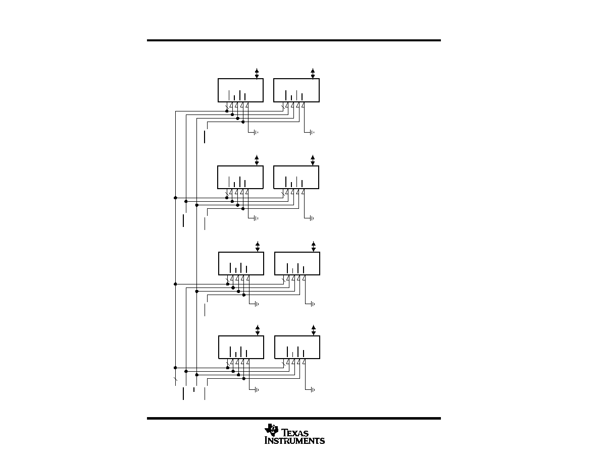
The TM124BBK32 operates as eight TMS44400DJs connected as shown in the functional block diagram. Refer
to the TMS44400 data sheet for details of operation. The common I/O feature of the TM124BBK32 dictates the
use of early write cycles to prevent contention on D and Q.
Copyright
©
1995, Texas Instruments Incorporated
PRODUCTION DATA information is current as of publication date.
Products conform to specifications per the terms of Texas Instruments
standard warranty. Production processing does not necessarily include
testing of all parameters.
Part numbers in this data sheet are for the gold-tabbed version; the information applies to both gold-tabbed and solder-tabbed versions.

TM124BBK32, TM124BBK32S 1048576 BY 32-BIT
TM248CBK32, TM248CBK32S 2097152 BY 32-BIT
DYNAMIC RAM MODULE
SMMS132D ≠ JANUARY 1991 ≠ REVISED JUNE 1995
2
POST OFFICE BOX 1443
∑
HOUSTON, TEXAS 77251≠1443
TM248CBK32
The TM248CBK32 operates as sixteen TMS44400DJs connected as shown in the functional block diagram.
Refer to the TMS44400 data sheet for details of operation. The common I/O feature of the TM248CBK32
dictates the use of early write cycles to prevent contention on D and Q.
refresh
Refresh period is extended to 16 ms and, during this period, each of the 1024 rows must be strobed with RAS
in order to retain data. A0-A9 address lines must be refreshed every 16 ms as required by the TMS44400 DRAM.
CAS can remain high during the refresh sequence to conserve power.
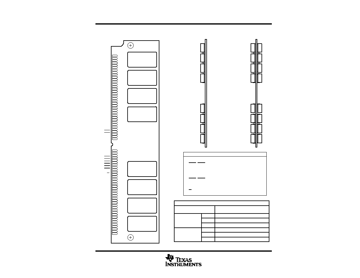
single in-line memory module and components
PC substrate: 1,27
±
0,1 mm (0.05 inch) nominal thickness; 0.005 inch/inch maximum warpage
Bypass capacitors: Multilayer ceramic
Contact area for TM124BBK32 AND TM248CBK32: Nickel plate and gold plate over copper.
Contact area for TM124BBK32S AND TM248CBK32S: Nickel plate and tin-lead over copper.