
TM124MBK36B, TM124MBK36R 1048576 BY 36-BIT
TM248NBK36B, TM248NBK36R 2097152 BY 36-BIT
DYNAMIC RAM MODULE
SMMS137E ≠ JANUARY 1991 ≠ REVISEDJUNE 1995
1
POST OFFICE BOX 1443
∑
HOUSTON, TEXAS 77251≠1443
D
Organization
TM124MBK36B . . . 1 048 576
◊
36
TM248NBK36B . . . 2 097 152
◊
36
D
Single 5-V Power Supply (
Ī
10% Tolerance)
D
72-pin Leadless Single In-Line Memory
Module (SIMM) for Use With Sockets
D
TM124MBK36B≠Utilizes Eight 4-Megabit
DRAMs in Plastic Small-Outline J-Lead
(SOJ) Packages and One 4-Megabit
Quad-CAS DRAM in a Plastic Small-Outline
J-Lead (SOJ) Package
D
TM248NBK36B≠Utilizes Sixteen 4-Megabit
DRAMs in Plastic Small-Outline J-Lead
(SOJ) Packages and Two 4-Megabit
Quad-CAS DRAMs in Plastic Small-Outline
J-Lead (SOJ) Packages
D
Long Refresh Period
16 ms (1024 Cycles)
D
All Inputs, Outputs, Clocks Fully TTL
Compatible
D
3-State Output
D
Common CAS Control for Nine Common
Data-In and Data-Out Lines, in Four Blocks
D
Enhanced Page Mode Operation with
CAS-Before-RAS ( CBR ), RAS-Only, and
Hidden Refresh
D
Presence Detect
D
Performance Ranges:
ACCESS
ACCESS ACCESS READ
TIME
TIME
TIME
OR
tRAC
tAA
tCAC
WRITE
CYCLE
(MAX) (MAX)
(MAX)
(MIN)
'124MBK36B-60 60 ns
30 ns
15 ns
110 ns
'124MBK36B-70 70 ns
35 ns
18 ns
130 ns
'124MBK36B-80 80 ns
40 ns
20 ns
150 ns
'248NBK36B-60
60 ns
30 ns
15 ns
110 ns
'248NBK36B-70
70 ns
35 ns
18 ns
130 ns
'248NBK36B-80
80 ns
40 ns
20 ns
150 ns
D
Low Power Dissipation
D
Operating Free-Air Temperature Range
0
į
C to 70
į
C
D
Gold-Tabbed Versions Available:
≠ TM124MBK36B
≠ TM248NBK36B
D
Tin-Lead (Solder) Tabbed Versions
Available:
≠ TM124MBK36R
≠ TM248NBK36R
description
TM124MBK36B
The TM124MBK36B is a dynamic random-access memory (DRAM) organized as four times 1 048 576
◊
9
(bit 9 is generally used for parity) in a 72-pin leadless single in-line memory module (SIMM). The SIMM is
composed of eight TMS44400DJ, 1 048 576
◊
4-bit DRAMs, each in 20/26-lead plastic small-outline J-lead
packages (SOJs), and one TMS44460DJ, 1 048 576
◊
4-bit Quad-CAS DRAM in a 24/26-lead plastic
small-outline J-lead package (SOJ), mounted on a substrate with decoupling capacitors. Each TMS44400DJ
and TMS44460DJ is described in the TMS44400 or TMS44460 data sheet, respectively.
The TM124MBK36B is available in the single-sided BK leadless module for use with sockets.
The TM124MBK36B features RAS access times of 60 ns, 70 ns, and 80 ns. This device is rated for operation
from 0
į
C to 70
į
C.
TM248NBK36B
The TM248NBK36B is a DRAM organized as four times 2 097 152
◊
9 (bit 9 is generally used for parity) in a
72-pin leadless SIMM. The SIMM is composed of sixteen TMS44400DJ, 1 048 576
◊
4-bit DRAMs, each in
20/26-lead plastic small-outline J-lead packages (SOJs), and two TMS44460DJ, 1 048 576
◊
4-bit Quad-CAS
DRAMs, each in a 24/26-lead plastic small-outline J-lead package (SOJ), mounted on a substrate with
decoupling capacitors. Each TMS44400DJ and TMS44460DJ is described in the TMS44400 and TMS44460
data sheet, respectively.
Copyright
©
1995, Texas Instruments Incorporated
Part numbers in this data sheet are for the gold-tabbed version; the information applies to both gold-tabbed and solder-tabbed versions.
PRODUCTION DATA information is current as of publication date.
Products conform to specifications per the terms of Texas Instruments
standard warranty. Production processing does not necessarily include
testing of all parameters.

TM124MBK36B, TM124MBK36R 1048576 BY 36-BIT
TM248NBK36B, TM248NBK36R 2097152 BY 36-BIT
DYNAMIC RAM MODULE
SMMS137E ≠ JANUARY 1991 ≠ REVISEDJUNE 1995
2
POST OFFICE BOX 1443
∑
HOUSTON, TEXAS 77251≠1443
TM248NBK36B (continued)
The TM124NBK36B is available in the double-sided BK leadless module for use with sockets.
The TM124NBK36B features RAS access times of 60 ns, 70 ns, and 80 ns. This device is rated for operation
from 0
į
C to 70
į
C
operation
TM124MBK36B
The TM124MBK36B operates as eight TMS44400DJs and one TMS44460DJ connected as shown in the
functional block diagram and Table 1. The parity bits are provided by the TMS44460DJ and are controlled by
RAS2. To ensure proper parity bit operation all memory accesses should include a RAS2 pulse. Refer to the
TMS44400 and TMS44460 data sheets for details of operation. The common I/O feature dictates the use of
early write cycles to prevent contention on D and Q.
TM248NBK36B
The TM248NBK36B operates as sixteen TMS44400DJs and two TMS44460DJs connected as shown in the
functional block diagram and Table 1. The parity bits are provided by the TMS44460DJ and are controlled by
RAS2 on side 1 and RAS3 on side 2. To ensure proper parity bit operation, all memory accesses should include
a RAS2 or RAS3 pulse. Refer to the TMS44400 and TMS44460 data sheets for details of operation. The
common I/O feature dictates the use of early write cycles to prevent contention on D and Q.
TM124MBK36B, TM124MBK36R 1048576 BY 36-BIT
TM248NBK36B, TM248NBK36R 2097152 BY 36-BIT
DYNAMIC RAM MODULE
SMMS137E ≠ JANUARY 1991 ≠ REVISEDJUNE 1995
3
POST OFFICE BOX 1443
∑
HOUSTON, TEXAS 77251≠1443
PRESENCE DETECT
SIGNAL
(PIN)
PD1
(67)
PD2
(68)
PD3
(69)
PD4
(70)
80 ns
VSS
VSS
NC
VSS
TM124MBK36B
70 ns
VSS
VSS
VSS
NC
60 ns
VSS
VSS
NC
NC
80 ns
NC
NC
NC
VSS
TM248NBK36B
70 ns
NC
NC
VSS
NC
60 ns
NC
NC
NC
NC
DQ17
DQ35
CAS0
CAS2
CAS3
CAS1
RAS0
RAS1
NC
W
NC
DQ9
DQ27
DQ10
DQ28
DQ11
DQ29
DQ12
DQ30
DQ13
DQ31
VCC
DQ32
DQ14
DQ33
DQ15
DQ34
DQ16
NC
PD1
PD2
PD3
PD4
NC
VSS
37
38
39
40
41
42
43
44
45
46
47
48
49
50
51
52
53
54
55
56
57
58
59
60
61
62
63
64
65
66
67
68
69
70
71
72
1
2
3
4
5
6
7
8
9
10
11
12
13
14
15
16
17
18
19
20
21
22
23
24
25
26
27
28
29
30
31
32
33
34
35
36
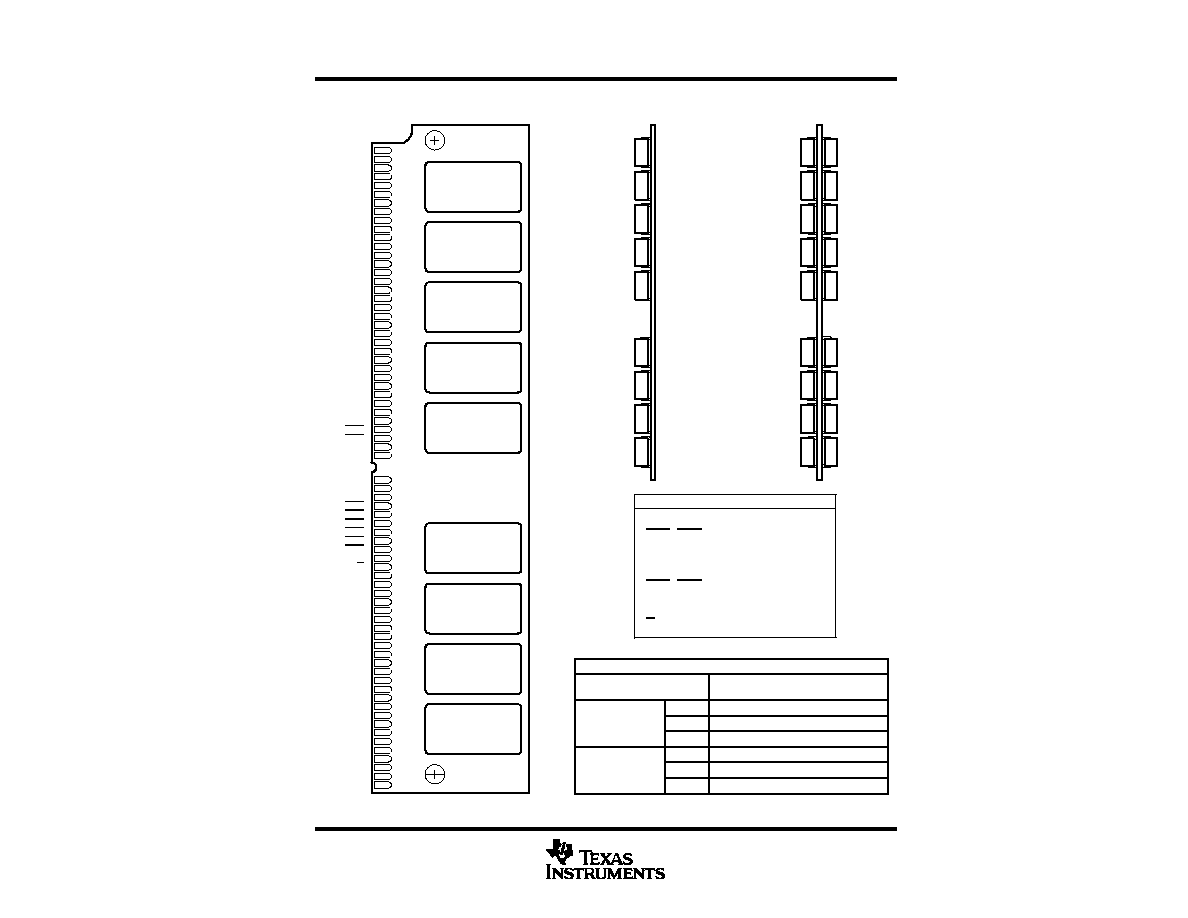
BK SINGLE IN-LINE MEMORY MODULE
(TOP VIEW)
TM124MBK36B
(SIDE VIEW)
PIN NOMENCLATURE
A0 ≠ A9
Address Inputs
CAS0 ≠ CAS3
Column-Address Strobe
DQ0 ≠ DQ35
Data In/Data Out
NC
No Connection
PD1 ≠ PD4
Presence Detects
RAS0 ≠ RAS3
Row-Address Strobe
VCC
5-V Supply
VSS
Ground
W
Write Enable
TM248NBK36B
(SIDE VIEW)
VSS
DQ0
DQ18
DQ1
DQ19
DQ2
DQ20
DQ3
DQ21
VCC
NC
A0
A1
A2
A3
A4
A5
A6
NC
DQ4
DQ22
DQ5
DQ23
DQ6
DQ24
DQ7
DQ25
A7
NC
VCC
A8
A9
RAS3
RAS2
DQ26
DQ8
VSS

TM124MBK36B, TM124MBK36R 1048576 BY 36-BIT
TM248NBK36B, TM248NBK36R 2097152 BY 36-BIT
DYNAMIC RAM MODULE
SMMS137E ≠ JANUARY 1991 ≠ REVISEDJUNE 1995
4
POST OFFICE BOX 1443
∑
HOUSTON, TEXAS 77251≠1443
Table 1. Connection Table
DATA BLOCK
RASx
CASx
DATA BLOCK
SIDE 1
SIDE 2
CASx
DQ0 ≠ DQ7
DQ8
RAS0
RAS2
RAS1
RAS3
CAS0
CAS0
DQ9 ≠ DQ16
DQ17
RAS0
RAS2
RAS1
RAS3
CAS1
CAS1
DQ18 ≠ DQ25
DQ26
RAS2
RAS2
RAS3
RAS3
CAS2
CAS2
DQ27 ≠ DQ34
DQ35
RAS2
RAS2
RAS3
RAS3
CAS3
CAS3
Side 2 applies to the TM248NBK36B only.
single-in-line memory module and components
PC substrate: 1,27
Ī
0,1 mm (0.05 inch) nominal thickness; 0.005 inch/inch maximum warpage
Bypass capacitors: Multilayer ceramic
Contact area for TM124MBK36B and TM248NBK36B: Nickel plate and gold plate over copper
Contact area for TM124MBK36R and TM248NBK36R: Nickel plate and tin-lead over copper
