
TMS320VC5420
FIXED POINT DIGITAL SIGNAL PROCESSOR
SPRS080E ≠ MARCH 1999 ≠ REVISED APRIL 2001
1
POST OFFICE BOX 1443
∑
HOUSTON, TEXAS 77251≠1443
D
200-MIPS Dual-Core DSP Consisting of Two
Independent Subsystems
D
Each Core Has an Advanced Multibus
Architecture With Three Separate 16-Bit
Data Memory Buses and One Program Bus
D
40-Bit Arithmetic Logic Unit (ALU)
Including a 40-Bit Barrel-Shifter and Two
40-Bit Accumulators Per Core
D
Each Core Has a 17-
◊
17-Bit Parallel
Multiplier Coupled to a 40-Bit Adder for
Non-Pipelined Single-Cycle Multiply/
Accumulate (MAC) Operations
D
Each Core Has a Compare, Select, and
Store Unit (CSSU) for the Add/Compare
Selection of the Viterbi Operator
D
Each Core Has an Exponent Encoder to
Compute an Exponent Value of a 40-Bit
Accumulator Value in a Single Cycle
D
Each Core Has Two Address Generators
With Eight Auxiliary Registers and Two
Auxiliary Register Arithmetic Units
(ARAUs)
D
16-Bit Data Bus With Data Bus Holder
Feature
D
256K
◊
16 Extended Program Address
Space
D
Total of 192K
◊
16 Dual- and Single-Access
On-Chip RAM
D
Single-Instruction Repeat and
Block-Repeat Operations
D
Instructions With 32-Bit Long Word
Operands
D
Instructions With 2 or 3 Operand Reads
D
Fast Return From Interrupts
D
Arithmetic Instructions With Parallel Store
and Parallel Load
D
Conditional Store Instructions
D
Output Control of CLKOUT
D
Output Control of TOUT
D
Power Consumption Control With IDLE1,
IDLE2, and IDLE3 Instructions
D
Dual 1.8-V (Core) and 3.3-V (I/O) Power
Supplies for Low Power, Fast Operation
D
10-ns Single-Cycle Fixed-Point Instruction
Execution
D
Interprocessor Communication via Two
Internal 8-Element FIFOs
D
12 Channels of Direct Memory Access
(DMA) for Data Transfers With No CPU
Loading (6 Channels Per Subsystem)
D
Six Multichannel Buffered Serial Ports
(McBSPs) (Three McBSPs Per Subsystem)
D
16-Bit Host-Port Interface (HPI16)
Multiplexed With External Memory Interface
Pins
D
Software-Programmable Phase-Locked
Loop (PLL) Provides Several Clocking
Options (Requires External TTL Oscillator)
D
On-Chip Scan-Based Emulation Logic
D
Two Software-Programmable Timers
(One Per Subsystem)
D
Software-Programmable Wait-State
Generator (14 Wait States Maximum)
D
Provided in 144-pin BGA Ball Grid Array
(GGU Suffix) and 144-pin Low-Profile Quad
Flatpack (LQFP) (PGE Suffix) Packages
NOTE: This data sheet is designed to be used in conjunction with the TMS320C54x
DSP Functional Overview (literature
number SPRU307).
Copyright
2001, Texas Instruments Incorporated
Please be aware that an important notice concerning availability, standard warranty, and use in critical applications of
Texas Instruments semiconductor products and disclaimers thereto appears at the end of this data sheet.
PRODUCTION DATA information is current as of publication date.
Products conform to specifications per the terms of Texas Instruments
standard warranty. Production processing does not necessarily include
testing of all parameters.
TMS320C54x is a trademark of Texas Instruments.
TMS320VC5420
FIXED POINT DIGITAL SIGNAL PROCESSOR
SPRS080E ≠ MARCH 1999 ≠ REVISED APRIL 2001
2
POST OFFICE BOX 1443
∑
HOUSTON, TEXAS 77251≠1443
Table of Contents
Description
3
. . . . . . . . . . . . . . . . . . . . . . . . . . . . . . . . . . . . . . .
Pin Assignments
6
. . . . . . . . . . . . . . . . . . . . . . . . . . . . . . . . . .
Signal Descriptions
10
. . . . . . . . . . . . . . . . . . . . . . . . . . . . . . .
Functional Overview
16
. . . . . . . . . . . . . . . . . . . . . . . . . . . . . .
Memory
17
. . . . . . . . . . . . . . . . . . . . . . . . . . . . . . . . . . . . . . . . .
Multicore Reset Signals
19
. . . . . . . . . . . . . . . . . . . . . . . . . . .
On-Chip Peripherals
21
. . . . . . . . . . . . . . . . . . . . . . . . . . . . . .
16-bit Host-Port Interface (HPI16)
24
. . . . . . . . . . . . . . . . . .
Multichannel Buffered Serial Port (McBSP)
26
. . . . . . . . . . .
Direct Memory Access Unit (DMA)
27
. . . . . . . . . . . . . . . . . .
Subsystem Communications
29
. . . . . . . . . . . . . . . . . . . . . . .
General-Purpose I/O
30
. . . . . . . . . . . . . . . . . . . . . . . . . . . . . .
Memory-Mapped Registers
33
. . . . . . . . . . . . . . . . . . . . . . . .
Interrupts
37
. . . . . . . . . . . . . . . . . . . . . . . . . . . . . . . . . . . . . . . .
IDLE3 Power-Down Mode
39
. . . . . . . . . . . . . . . . . . . . . . . . .
Emulating the 5420 Device
39
. . . . . . . . . . . . . . . . . . . . . . . .
Documentation Support
40
. . . . . . . . . . . . . . . . . . . . . . . . . . .
Absolute Maximum Ratings
41
. . . . . . . . . . . . . . . . . . . . . . . .
Recommended Operating Conditions
41
. . . . . . . . . . . . . . .
Electrical Characteristics
42
. . . . . . . . . . . . . . . . . . . . . . . . . .
External Multiply-By-N Clock Option
43
. . . . . . . . . . . . . . . .
Bypass Option
44
. . . . . . . . . . . . . . . . . . . . . . . . . . . . . . . . . . .
External Memory Interface Timing for One Wait State
45
. .
Ready Timing for Externally Generated Wait States
49
. . .
Parallel I/O Interface Timing
51
. . . . . . . . . . . . . . . . . . . . . . .
I/O Port Timing for Externally Generated Wait States
53
. .
Reset, BIO, Interrupt, and XIO Timing
55
. . . . . . . . . . . . . . .
External Flag (XF) and Timer Output (TOUT) Timing
57
. .
General-Purpose Input/Output (GPIO) Timing
58
. . . . . . . .
SELA/B Timing
59
. . . . . . . . . . . . . . . . . . . . . . . . . . . . . . . . . . .
Multichannel Buffered Serial Port Timing
60
. . . . . . . . . . . . .
HPI16 Timing
68
. . . . . . . . . . . . . . . . . . . . . . . . . . . . . . . . . . . .
Mechanical Data
76
. . . . . . . . . . . . . . . . . . . . . . . . . . . . . . . . .
REVISION HISTORY
REVISION
DATE
PRODUCT STATUS
HIGHLIGHTS
*
March 1999
Advance Information
Original
A
April 1999
Advance Information
Updated characteristics data.
B
September 1999
Production Data
Updated characteristics data.
C
April 2000
Production Data
Updated characteristics data.
D
June 2000
Production Data
Updated characteristics data.
E
April 2001
Production Data
Removed 4K
◊
16-bit block of on-chip memory labeled SARAM4.
This is no longer a supported feature of this device.

TMS320VC5420
FIXED POINT DIGITAL SIGNAL PROCESSOR
SPRS080E ≠ MARCH 1999 ≠ REVISED APRIL 2001
3
POST OFFICE BOX 1443
∑
HOUSTON, TEXAS 77251≠1443
description
The TMS320VC5420 fixed-point digital signal processor (DSP) is a dual CPU device capable of up to 200-MIPS
performance. The 5420 consists of two independent 54x subsystems capable of core-to-core communications.
Each subsystem CPU is based on an advanced, modified Harvard architecture that has one program memory
bus and three data memory buses. The processor also provides an arithmetic logic unit (ALU) that has a high
degree of parallelism, application-specific hardware logic, on-chip memory, and additional on-chip peripherals.
Each subsystem has separate program and data spaces, allowing simultaneous accesses to program
instructions and data. Two read operations and one write operation can be performed in one cycle. Instructions
with parallel store and application-specific instructions can fully utilize this architecture. Furthermore, data can
be transferred between program and data spaces. Such parallelism supports a powerful set of arithmetic, logic,
and bit manipulation operations that can be performed in a single machine cycle. In addition, the 5420 includes
the control mechanisms to manage interrupts, repeated operations, and function calls.
The 5420 is offered in two temperature ranges and individual part numbers as shown below. (Please note that
the industrial temperature device part numbers do not follow the typical numbering tradition.)
Commercial temperature devices (0
∞
C to 100
∞
C)
TMS320VC5420PGE200 (144-pin LQFP)
TMS320VC5420GGU200 (144-pin BGA)
Industrial temperature range devices (≠40
∞
C to 100
∞
C)
TMS320C5420PGEA200 (144-pin LQFP)
TMS320C5420GGUA200 (144-pin BGA)
TMS320VC5420
FIXED POINT DIGITAL SIGNAL PROCESSOR
SPRS080E ≠ MARCH 1999 ≠ REVISED APRIL 2001
4
POST OFFICE BOX 1443
∑
HOUSTON, TEXAS 77251≠1443
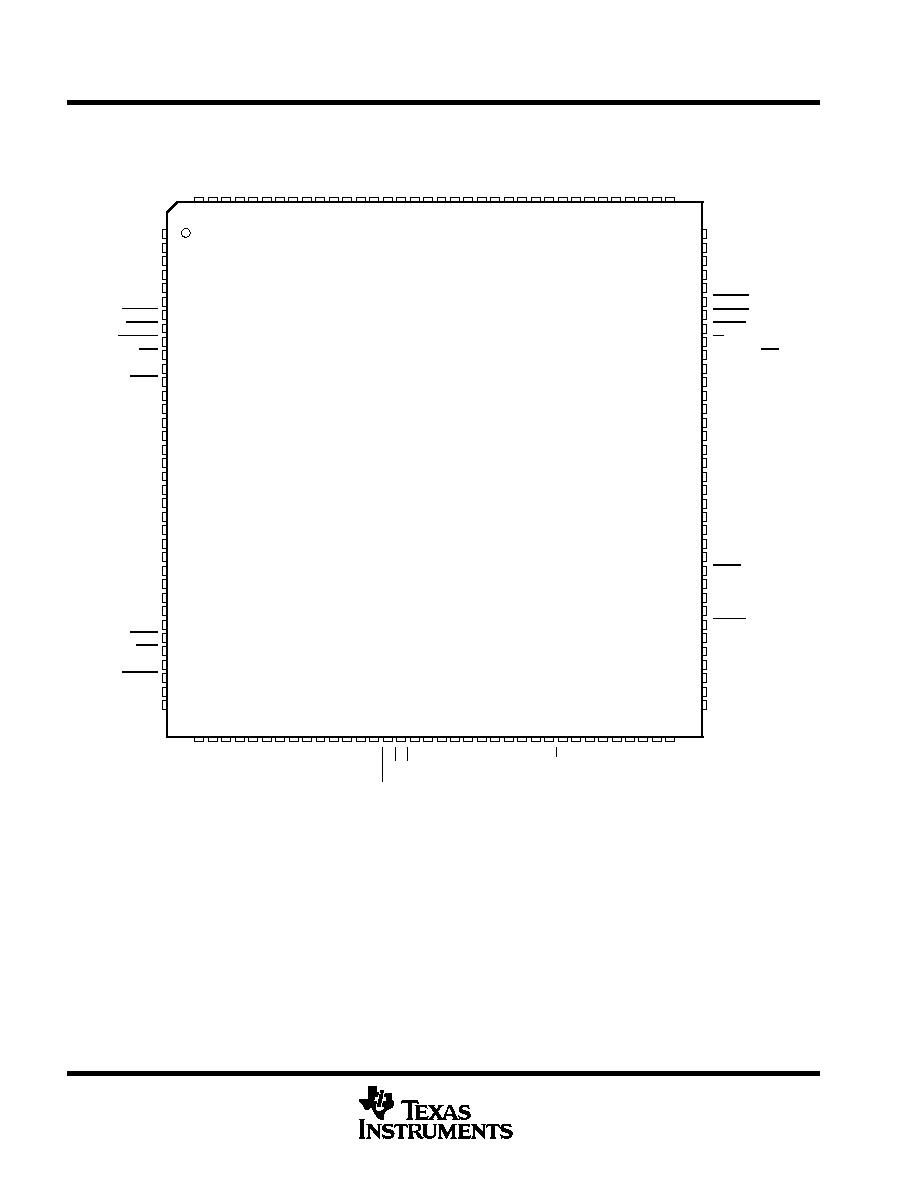
AV
PPA14
PPA15
VSS
PPA16
PPA17
B_INT0
B_INT1
B_NMI
IS
B_GPIO2/BIO
B_GPIO1
B_GPIO0
B_BFSR1
B_BDR1
CVDD
VSS
B_BCLKR1
B_BFSX1
VSS
B_BDX1
B_BCLKX1
CVDD
VSS
TEST
XIO
B_RS
B_XF
B_CLKOUT
HMODE
HPIRS
PPA13
PPA12
VSS
DVDD
PPA11
PPA10
PPD7
PPA8
PPA0
DVDD
PPA9
PPD1
A_INT1
A_NMI
IOSTRB
A_GPIO2/BIO
A_GPIO1
A_RS
A_GPIO0
VSS
VSS
CVDD
A_BFSR1
A_BDR1
A_BCLKR1
A_BFSX1
CVDD
VSS
A_BDX1
A_BCLKX1
A_XF
A_CLKOUT
VCO
TCK
TMS
TDI
TRST
EMU1/OFF
DVDD
A_INT0
EMU0
TDO
144
PPD0
PPD5
143
142
141
PPD6
140
A_BFSX2
139
A_BDX2
138
A_BFSR2
137
A_BDR2
136
A_BCLKR2
135
134
133
A_BCLKX2
132
READY
131
DV
130
129
128
127
126
125
B_BCLKX2
124
B_BDX2
123
B_BFSX2
122
B_BCLKR2
121
120
11
9
B_BDR2
11
8
11
7
PPD2
11
6
PPD3
11
5
PP
A1
11
4
PP
A5
11
3
11
2
37
38
39
40
41
42
43
44
45
46
47
48
49
50
51
52
53
54
55
56
57
58
59
60
61
62
63
64
65
66
67
68
69
1
2
3
4
5
6
7
8
9
10
11
12
13
14
15
16
17
18
19
20
21
22
23
24
25
26
27
28
29
30
31
32
33
34
35
36
108
107
106
105
104
103
102
101
100
99
98
97
96
95
94
93
92
91
90
89
88
87
86
85
84
83
82
81
80
79
78
77
76
75
74
73
PPD15
PPD14
SS
PPD13
PPD12
A_BFSR0
A_BDR0
A_BCLKR0
A_BFSX0
A_BDX0
A_BCLKX0
DD
SS
B_BFSX0
B_BCLKR0
B_BDR0
B_BFSR0
R/W
PP
A2
PP
A3
SELA/B
PPD8
PPD9
PPD10
B_BDX0
MSTRB
111
11
0
PP
A7
109
70
71
72
PPD1
1
B_BFSR2
PP
A6
DV
CLKIN
V
DV
V
DD
DD
DD
TMS320VC5420 PGE PACKAGEß
(TOP VIEW)
PPD4
B_BCLKX0
SS
V
V
SS
SS
V
SS
V
SS
V
DD
CV
DS
PS
DD
CV
SS
V
PP
A4
SS
V
CV
DD
SSA
V
NC
CV
DD
SS
V
NC = No internal connection
DVDD is the power supply for the I/O pins while CVDD is the power supply for the core CPU. VSS is the ground for both the I/O
pins and the core CPU.
ß Pin configuration shown for nonmultiplexed mode only. See the Pin Assignments for the TMS320VC5420PGE table for multiplexed
functions of specific pins.
TMS320VC5420
FIXED POINT DIGITAL SIGNAL PROCESSOR
SPRS080E ≠ MARCH 1999 ≠ REVISED APRIL 2001
5
POST OFFICE BOX 1443
∑
HOUSTON, TEXAS 77251≠1443
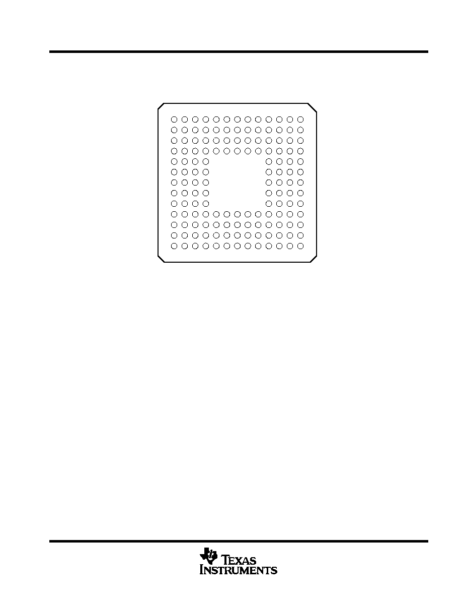
TMS320VC5420 GGU PACKAGE
(BOTTOM VIEW)
A
B
D
C
E
F
H
J
L
M
K
N
G
1
2
3
4
5
6
7
8
10
12 11
13
9
The pin assignments table for the TMS320VC5420GGU lists each pin name and its associated pin number for
this 144-pin ball grid array (BGA) package.