
TMS320WP010
DIGITAL SIGNAL PROCESSOR
FOR AEC/LEC/ANS
SPRS040≠OCTOBER 1995
1
POST OFFICE BOX 655303
∑
DALLAS, TEXAS 75265
D
Cancels the Acoustic Echo Common in
Hands-Free Use of Cellular Phones in
Automobiles
≠ Eliminates Echo Created by Speaker
Output Feeding Back Into the
Microphone
D
Suppresses Wind, Engine, and Tire Noise
D
Line Echo Canceler
D
Standard Independent
≠ IS-54B, IS-136, GSM, AMPS, IS-95
D
Continuous, Automatic Adaptation to
Changing Acoustic Environment
≠ Initial System Training Not Required
D
Based on TMS320C5x Platforms
D
Support for Industry Standard
Microcontrollers
D
Interfaces Easily with TI's Voice Codec, the
TCM320AC36
D
Acoustic Echo Canceler Performance
≠ Length of Echo Path up to 44 ms
≠ Initial Adaptation Rate
>
20 dB/s for
Speech Signals
≠ Zero Speech Delay
≠ Echo Return Loss up to 30 dB for
Speech Echo in Automobiles and 41 dB
for Sine Wave Input
D
Noise Suppressor Performance
≠ Up to 10 dB Noise Suppression for
Hands-Free Use of Cellular Phones in
Automobiles Without Distorting Speech
Signals
≠ 16 ms Processing Delay
≠ Continuous Adaptation
D
Demonstration Platform
≠ Allows Evaluation of Software Algorithm
Performance in Lab and Automobile
≠ Ability to Enable/Disable AEC, ANS, and
LEC
description
For the cellular phone cradle market, the TMS320WP010 provides enhanced quality, full-duplex, hands-free
communications. The 'WP010 is a ROM-coded DSP that provides all the adaptive filtering and processing
necessary for acoustic echo cancellation (AEC), line echo cancellation (LEC), and adaptive noise suppression
(ANS).
The 'WP010's acoustic echo cancellation function is based on a Finite Impulse Response (FIR) filter with an
adaptive coefficient updating algorithm. The adaptive algorithm updates continuously so that it can constantly
track acoustic path changes from the speaker to the microphone. Based upon FIR filter coefficients, the echo
signal can be estimated and subtracted from the observed signal at the microphone. The acoustic echo
cancellation function provides continuous adaptation and needs no initial system training. It is capable of
canceling an echo path of up to 44 milliseconds and provides up to 30 dB cancellation for speech signals. In
addition, the initial convergence rate is faster than 20 dB per second.
The line echo cancellation function cancels the near-end speech that has been reflected at the network switch
and transmitted back to the cellular phone. The principle of the line echo cancellation function is very similar
to that of the acoustic echo cancellation function. The difference is that the line echo cancellation function is
designed to cancel the echo signal caused by network feedback due to impedance mismatch in the network
circuit. The line echo cancellation function is capable of canceling a line echo path of up to 16 milliseconds.
The received signal at the microphone consists of the near-end speech signal, acoustic feedback echo, and
ambient noise from the environment. The purpose of the adaptive noise suppression function is to suppress
ambient noise components without distorting near-end speech. The initial adaptation rate is about 3 dB per
second without initial system training. It tracks the changes of the noise characteristics and suppresses noise
accordingly. The adaptive noise suppression provides up to 10 dB of noise cancellation without degrading
near-end speech.
Please be aware that an important notice concerning availability, standard warranty, and use in critical applications of
Texas Instruments semiconductor products and disclaimers thereto appears at the end of this data sheet.
PRODUCTION DATA information is current as of publication date.
Products conform to specifications per the terms of Texas Instruments
standard warranty. Production processing does not necessarily include
testing of all parameters.
Copyright
©
1995, Texas Instruments Incorporated

TMS320WP010
DIGITAL SIGNAL PROCESSOR
FOR AEC/LEC/ANS
SPRS040≠OCTOBER 1995
2
POST OFFICE BOX 655303
∑
DALLAS, TEXAS 75265
HOLDA
TMS320WP010
PZ PACKAGE
( TOP VIEW )
EMU1/ OFF
V
SSC
RS
READY
HOLD
BIO
TRST
V
SSI
MP/ MC
D15
D14
D12
D11
D10
D9
D8
V
DDD
18
25
24
23
22
21
20
19
17
16
15
14
13
12
11
10
9
8
7
6
5
4
3
2
1
EMU0
TOUT
D13
V
SSI
58
51
52
53
54
55
56
57
59
60
61
62
63
64
65
66
67
68
69
70
71
72
73
74
75
RD
V
DDA
A15
A14
A13
A12
A11
A10
CLKMD1
V
SSA
V
SSA
V
DDI
A9
A8
A7
A5
A4
A3
A2
A1
WE
A6
TDI
A0
100 99 98 97 96 95 94 93 92 91 90 89 88 87 86 85 84 83 82 81 80 79 78 77 76
DDC
V
CLKOUT1
XF
DX2
DX1
CLKMD2
TDO
CLKIN2
BR
R/W
DS
X1
STRB
PS
IS
26 27 28 29 30 31 32 33 34 35 36 37 38 39 40 41 42 43 44 45 46 47 48 49 50
FSX1
X2
/
CLKIN
V
SSA
CLKX2
CLKX1
FSR2
CLKR2
FSX2
V
SSD
V
SSD
D7
D6
D5
D4
D3
D2
D1
D0
TMS
V
DDD
TCK
V
SSD
V
SSD
INT1
INT2
INT3
INT4
NMI
DR1
DR2
FSR1
CLKR1
V
DDA
DDI
V
DDI
V
SSI
V
SSI
V
SSC
V
DDC
V

TMS320WP010
DIGITAL SIGNAL PROCESSOR
FOR AEC/LEC/ANS
SPRS040≠OCTOBER 1995
3
POST OFFICE BOX 655303
∑
DALLAS, TEXAS 75265
Pin Functions for Devices in the PZ Package
SIGNAL
TYPE
DESCRIPTION
PARALLEL INTERFACE BUS
A0 ≠ A15
I / O / Z
16-bit external address bus (MSB: A15, LSB: A0)
D0 ≠ D15
I / O / Z
16-bit external data bus (MSB: D15, LSB: D0)
PS, DS, IS
O / Z
Program, data, and I /O space select outputs, respectively
STRB
I / O / Z
Timing strobe for external cycles and external DMA
R / W
I / O / Z
Read / write select for external cycles and external DMA
RD, WE
O / Z
Read and write strobes, respectively, for external cycles
READY
I
External bus ready/ wait-state control input
BR
I / O / Z
Bus request. Arbitrates global memory and external DMA
SYSTEM INTERFACE / CONTROL SIGNALS
RS
I
Reset. Initializes device and sets PC to zero
MP/ MC
I
Microprocessor/microcomputer mode select. Enables internal ROM
HOLD
I
Puts parallel I/ F bus in high-impedance state after current cycle
HOLDA
O / Z
Hold acknowledge. Indicates external bus in hold state
XF
O / Z
External flag output. Set /cleared through software
BIO
I
I /O branch input. Implements conditional branches
TOUT
O / Z
Timer output signal. Indicates output of internal timer
INT1 ≠ INT4
I
External interrupt inputs
NMI
I
Nonmaskable external interrupt
SERIAL PORT INTERFACE
DR1, DR2
I
Serial receive-data input
DX1, DX2
O / Z
Serial transmit-data output. In high-impedance state when not transmitting
CLKR1, CLKR2
I
Serial receive-data clock input
CLKX1, CLKX2
I / O / Z
Serial transmit-data clock. Internal or external source
FSR1, FSR2
I
Serial receive-frame-synchronization input
FSX1, FSX2
I / O / Z
Serial transmit-frame-synchronization signal. Internal or external source
LEGEND:
I = Input
O = Output
Z = High impedance

TMS320WP010
DIGITAL SIGNAL PROCESSOR
FOR AEC/LEC/ANS
SPRS040≠OCTOBER 1995
4
POST OFFICE BOX 655303
∑
DALLAS, TEXAS 75265
Pin Functions for Devices in the PZ Package (Continued)
SIGNAL
TYPE
DESCRIPTION
EMULATION/JTAG INTERFACE
TDI
I
JTAG-test-port scan data input
TDO
O / Z
JTAG-test-port scan data output
TMS
I
JTAG-test-port mode select input
TCK
I
JTAG-port clock input
TRST
I
JTAG-port reset (with pull-down resistor). Disables JTAG when low
EMU0
I / O / Z
Emulation control 0. Reserved for emulation use
EMU1 / OFF
I / O / Z
Emulation control 1. Puts outputs in high-impedance state when low
CLOCK GENERATION AND CONTROL
X1
O
Oscillator output
X2 / CLKIN
I
Clock/oscillator input
CLKIN2
I
Clock input
CLKMD1, CLKMD2
I
Clock-mode select inputs
CLKOUT1
I / O / Z
Device system-clock output
POWER SUPPLY CONNECTIONS
VDDA
S
Supply connection, address-bus output
VDDD
S
Supply connection, data-bus output
VDDC
S
Supply connection, control output
VDDI
S
Supply connection, internal logic
VSSA
S
Supply connection, address-bus output
VSSD
S
Supply connection, data-bus output
VSSC
S
Supply connection, control output
VSSI
S
Supply connection, internal logic
LEGEND:
I = Input
O = Output
S = Supply
Z = High impedance
TMS320WP010
DIGITAL SIGNAL PROCESSOR
FOR AEC/LEC/ANS
SPRS040≠OCTOBER 1995
5
POST OFFICE BOX 655303
∑
DALLAS, TEXAS 75265
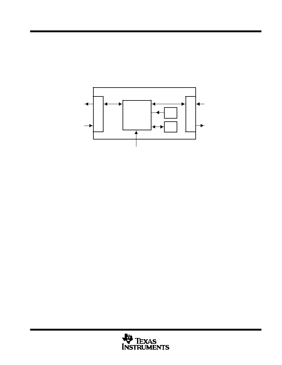
architecture
The 'WP010 architecture is based on the TMS320C5x Digital Signal Processor as shown in Figure 1. The
'WP010 sends/receives data through two serial ports available in the device. The first serial port (both RX1 and
TX1) should be connected to the audio codec to interface with the phone line (in the cradle). The other serial
port (RX2 and TX2) should be connected to the audio codec for the microphone and the speaker interfaces.
The necessary software for the 'WP010 is ROM-coded and contained in ROM space. The 'WP010 also provides
an MCU control interface to receive control commands from an MCU. The MCU control commands include the
ability to reset the 'WP010 and to enable/disable some functions of the 'WP010.
DSP Core
TMS320C5X
MCU Control
Serial Port
Serial Port
RAM
ROM
TX1
RX1
To Audio
Codec
TX2
RX2
To Audio
Codec
Figure 1. TMS320WP010 Architecture
functional description
The 'WP010 contains three main functional blocks: the adaptive line echo canceler, the adaptive acoustic echo
canceler, and the adaptive noise suppressor. All three functions can be enabled or disabled by MCU control
commands.
line echo canceler
The line echo canceler is to cancel the feedback line echo between two ports: RX1 and TX1. This function is
performed by estimating the line echo path adaptively and subtracting it from the input signal. The line echo
canceler cancels up to 16 milliseconds of line echo.
acoustic echo canceler
The purpose of the acoustic echo canceler (AEC) is to cancel the feedback acoustic echo from TX2 (interfaced
with the speaker) to RX2 (interfaced with the microphone). The signal from the microphone (via RX2) is
subtracted from the estimate of the acoustic echo path. The acoustic echo canceler is capable of canceling an
echo up to 44 milliseconds long.
adaptive noise suppressor
The purpose of the adaptive noise suppressor (ANS) is to selectively suppress noise from the signal coming
from the microphone (via RX2) without distorting near-end speech. Near-end speech is the desired speech
signal of the user of the hands-free phone in a car. The adaptive noise suppressor tracks noise characteristics
and suppresses accordingly. The ANS can suppress noise up to 10 dB.
development support
Texas Instruments offers a demonstration platform for the 'WP010. This platform contains all software modules
including AEC, LEC, and ANS. There are switches that allow the algorithms to be turned on and off. The
demonstration platform can be used in a lab or an automobile to fully evaluate the performance of the 'WP010.