 | –≠–ª–µ–∫—Ç—Ä–æ–Ω–Ω—ã–π –∫–æ–º–ø–æ–Ω–µ–Ω—Ç: TMS417400 | –°–∫–∞—á–∞—Ç—å:  PDF PDF  ZIP ZIP |

Please be aware that an important notice concerning availability, standard warranty, and use in critical applications of
Texas Instruments semiconductor products and disclaimers thereto appears at the end of this data sheet.
TMS416400, TMS416400P, TMS417400, TMS417400P
TMS426400, TMS426400P, TMS427400, TMS427400P
4194304-WORD BY 4-BIT HIGH-SPEED DRAMS
SMKS881B ≠ MAY 1995 ≠ REVISED AUGUST 1995
1
POST OFFICE BOX 1443
∑
HOUSTON, TEXAS 77251≠1443
Electrical characteristics for TMS416400 / P and
TMS417400 / P is Production Data. Electrical
characteristics for TMS426400 / P and
TMS427400 / P is Product Preview only.
D
Organization . . . 4 194 304
◊
4
D
Single 5 V Power Supply for TMS41x400 / P
(
±
10% Tolerance)
D
Single 3.3 V Power Supply for
TMS42x400 / P (
±
0.3 V Tolerance)
D
Performance Ranges:
ACCESS ACCESS ACCESS READ OR
TIME
TIME
TIME
WRITE
tRAC
tCAC
tAA
CYCLE
MAX
MAX
MAX
MIN
'4xx400/P-60
60 ns
15 ns
30 ns
110 ns
'4xx400/P-70
70 ns
18 ns
35 ns
130 ns
'4xx400/P-80
80 ns
20 ns
40 ns
150 ns
D
Enhanced Page-Mode Operation With
CAS-Before-RAS ( CBR ) Refresh
D
Long Refresh Period and Self-Refresh
Option ( TMS4xx400P)
D
3-State Unlatched Output
D
Low Power Dissipation
D
High-Reliability Plastic 24 / 26-Lead
300-Mil-Wide Surface-Mount Small-Outline
J-Lead (SOJ) Package and 24 / 26-Lead
Surface-Mount Thin Small-Outline Package
( TSOP)
D
Operating Free-Air Temperature Range:
0
∞
C to 70
∞
C
D
EPIC
TM
(Enhanced Performance Implanted
CMOS) Technology
AVAILABLE OPTIONS
DEVICE
POWER
SUPPLY
SELF
REFRESH
BATTERY
BACKUP
REFRESH
CYCLES
TMS416400
TMS416400P
TMS417400
TMS417400P
TMS426400
TMS426400P
TMS427400
TMS427400P
5 V
5 V
5 V
5 V
3.3 V
3.3 V
3.3 V
3.3 V
--
Yes
--
Yes
--
Yes
--
Yes
4096 in 64 ms
4096 in 128 ms
2048 in 32 ms
2048 in 128 ms
4096 in 64 ms
4096 in 128 ms
2048 in 32 ms
2048 in 128 ms
These devices feature maximum RAS access times of 60 ns, 70 ns, and 80 ns. All addresses and data-in lines
are latched on-chip to simplify system design. Data out is unlatched to allow greater system flexibility.
See Available Options Table
PIN NOMENCLATURE
A0 ≠ A11
Address Inputs
CAS
Column-Address Strobe
DQ1 ≠ DQ4
Data In / Data Out
OE
Output Enable
NC
No Internal Connection
RAS
Row-Address Strobe
VCC
5-V or 3.3-V Supply
VSS
Ground
W
Write Enable
DJ PACKAGE
( TOP VIEW )
V
CC
DQ1
DQ2
W
RAS
A0
A1
A2
A3
V
CC
V
SS
DQ4
DQ3
CAS
OE
A7
A6
A5
A4
V
SS
26
25
24
23
22
18
17
16
15
14
1
2
3
4
5
9
10
11
12
13
A11
A9
21
6
A10
A8
19
8
DGA PACKAGE
( TOP VIEW )
V
CC
DQ1
DQ2
W
RAS
A0
A1
A2
A3
V
CC
V
SS
DQ4
DQ3
CAS
OE
A7
A6
A5
A4
V
SS
26
25
24
23
22
18
17
16
15
14
1
2
3
4
5
9
10
11
12
13
A11
A9
21
6
A10
A8
19
8
A11 is NC for TMS4x7400 / P.
description
The TMS4xx400 is a set of high-speed,
16 777 216-bit dynamic random-access memories
organized as 4 194 304 words of 4 bits each. The
TMS4xx400P series are high-speed, low-power,
self-refresh, 16 777 216-bit dynamic random-
access memories organized as 4 194 304 words of
4 bits each. The TMS4xx400 and TMS4xx400P
employ state-of-the-art EPIC
TM
(Enhanced
Performance Implanted CMOS) technology for
high performance, reliability, and low power.
UNLESS OTHERWISE NOTED this document contains PRODUCTION
DATA information current as of publication date. Products conform to
specifications per the terms of Texas Instruments standard warranty.
Production processing does not necessarily include testing of all
parameters.
Copyright
©
1995, Texas Instruments Incorporated
EPIC is a trademark of Texas Instruments Incorporated.

TMS416400, TMS416400P, TMS417400, TMS417400P
TMS426400, TMS426400P, TMS427400, TMS427400P
4194304-WORD BY 4-BIT HIGH-SPEED DRAMS
SMKS881B ≠ MAY 1995 ≠ REVISED AUGUST 1995
2
POST OFFICE BOX 1443
∑
HOUSTON, TEXAS 77251≠1443
description (continued)
The TMS4xx400 and TMS4xx400P are each offered in a 24 / 26-lead plastic surface-mount TSOP (DGA suffix)
package and a 24 / 26-lead plastic surface-mount SOJ (DJ suffix) package. These packages are characterized
for operation from 0
∞
C to 70
∞
C.
operation
enhanced page mode
Enhanced page-mode operation allows faster memory access by keeping the same row address while selecting
random column addresses. The time for row-address setup and hold and address multiplex is eliminated. The
maximum number of columns that can be accessed is determined by t
RASP
, the maximum RAS low time.
Unlike conventional page-mode DRAMs, the column-address buffers in these devices are activated on the
falling edge of RAS. The buffers act as transparent or flow-through latches while CAS is high. The falling edge
of CAS latches the column addresses and enables the output. This feature allows the devices to operate at a
higher data bandwidth than conventional page-mode parts because data retrieval begins as soon as the column
address is valid rather than when CAS transitions low. This performance improvement is referred to as
enhanced page mode. A valid column address can be presented immediately after row-address hold time has
been satisfied, usually well in advance of the falling edge of CAS. In this case, data is obtained after t
CAC
max
(access time from CAS low) if t
AA
max (access time from column address) and t
RAC
have been satisfied. In the
event that column address for the next cycle is valid at the time CAS goes high, access time for the next cycle
is determined by the later occurrence of t
CPA
or t
CAC
.
address: A0 ≠ A11 ( TMS4x6400 / P) and A0 ≠ A10 (TMS4x7400 / P)
Twenty-two address bits are required to decode 1 of 4 194 304 storage cell locations. For the TMS4x6400 and
TMS4x6400P, 12 row-address bits are set up on A0 through A11 and latched onto the chip by the row-address
strobe (RAS). Ten column-address bits are set up on A0 through A9. For TMS4x7400 and TMS4x7400P, 11
row-address bits are set up on inputs A0 through A10 and latched onto the chip by RAS. Eleven column-address
bits are set up on A0 through A10. All addresses must be stable on or before the falling edge of RAS and CAS.
RAS is similar to a chip enable because it activates the sense amplifiers as well as the row decoder. CAS is used
as a chip select, activating the output buffers and latching the address bits into the column-address buffers.
write enable ( W )
The read or write mode is selected through W. A logic high on W selects the read mode, and a logic low selects
the write mode. The data inputs are disabled when the read mode is selected. When W goes low prior to CAS
(early write), data out remains in the high-impedance state for the entire cycle, permitting a write operation with
OE grounded.
data in (DQ1 ≠ DQ4)
Data is written during a write or read-modify-write cycle. Depending on the mode of operation, the falling edge
of CAS or W strobes data into the on-chip data latch. In an early-write cycle, W is brought low prior to CAS, and
the data is strobed in by CAS with setup and hold times referenced to this signal. In a delayed-write or
read-modify-write cycle, CAS is already low, and the data is strobed in by W with setup and hold time referenced
to this signal. In a delayed-write or read-modify-write cycle, OE must be high to bring the output buffers to the
high-impedance state prior to impressing data on the I/O lines.
data out (DQ1 ≠ DQ4)
Data out is the same polarity as data in. The output is in the high-impedance (floating) state until CAS and OE
are brought low. In a read cycle, the output becomes valid after the access time interval t
CAC
(which begins with
the negative transition of CAS) as long as t
RAC
and t
AA
are satisfied.

TMS416400, TMS416400P, TMS417400, TMS417400P
TMS426400, TMS426400P, TMS427400, TMS427400P
4194304-WORD BY 4-BIT HIGH-SPEED DRAMS
SMKS881B ≠ MAY 1995 ≠ REVISED AUGUST 1995
3
POST OFFICE BOX 1443
∑
HOUSTON, TEXAS 77251≠1443
RAS-only refresh
TMS4x6400, TMS4x6400P
A refresh operation must be performed at least once every 64 ms (128 ms for TMS4x6400P) to retain data. This
can be achieved by strobing each of the 4096 rows (A0 ≠ A11). A normal read or write cycle refreshes all bits
in each row that is selected. A RAS-only operation can be used by holding CAS at the high (inactive) level,
conserving power as the output buffers remain in the high-impedance state. Externally generated addresses
must be used for a RAS-only refresh.
TMS4x7400, TMS4x7400P
A refresh operation must be performed at least once every 32 ms (128 ms for TMS4x7400P) to retain data. This
can be achieved by strobing each of the 2048 rows (A0 ≠ A10). A normal read or write cycle refreshes all bits
in each row that is selected. A RAS-only operation can be used by holding CAS at the high (inactive) level,
conserving power as the output buffers remain in the high-impedance state. Externally generated addresses
must be used for a RAS-only refresh.
hidden refresh
Hidden refresh can be performed while maintaining valid data at the output pin. This is accomplished by holding
CAS at V
IL
after a read operation and cycling RAS after a specified precharge period, similar to a RAS-only
refresh cycle. The external address is ignored, and the refresh address is generated internally.
CAS-before-RAS ( CBR ) refresh
CBR refresh is utilized by bringing CAS low earlier than RAS (see parameter t
CSR
) and holding it low after RAS
falls (see parameter t
CHR
). For successive CBR refresh cycles, CAS can remain low while cycling RAS. The
external address is ignored, and the refresh address is generated internally.
battery-backup refresh
TMS4x6400P
A low-power battery-backup refresh mode that requires less than 500
µ
A (5 V ) or 350
µ
A (3.3 V ) refresh current
is available on the TMS4x6400P. Data integrity is maintained using CBR refresh with a period of 31.25
µ
s while
holding RAS low for less than 1
µ
s. To minimize current consumption, all input levels must be at CMOS levels
( V
IL
<
0.2 V, V
IH
>
V
CC
≠ 0.2 V ).
TMS4x7400P
A low-power battery-backup refresh mode that requires less than 500
µ
A (5 V ) or 350
µ
A (3.3 V ) refresh current
is available on the TMS4x7400P. Data integrity is maintained using CBR refresh with a period of 62.5
µ
s while
holding RAS low for less than 1
µ
s. To minimize current consumption, all input levels must be at CMOS levels
( V
IL
<
0.2 V, V
IH
>
V
CC
≠ 0.2 V ).
self refresh ( TMS4xx400P)
The self-refresh mode is entered by dropping CAS low prior to RAS going low. Then CAS and RAS are both
held low for a minimum of 100
µ
s. The chip is then refreshed internally by an on-board oscillator. No external
address is required because the CBR counter is used to keep track of the address. To exit the self-refresh mode,
both RAS and CAS are brought high to satisfy t
CHS
. Upon exiting self-refresh mode, a burst refresh (refresh a
full set of row addresses) must be executed before continuing with normal operation. The burst refresh ensures
the DRAM is fully refreshed.
power up
To achieve proper device operation, an initial pause of 200
µ
s followed by a minimum of eight initialization cycles
is required after power up to the full V
CC
level. These eight initialization cycles must include at least one refresh
( RAS-only or CBR ) cycle.
TMS416400, TMS416400P, TMS417400, TMS417400P
TMS426400, TMS426400P, TMS427400, TMS427400P
4194304-WORD BY 4-BIT HIGH-SPEED DRAMS
SMKS881B ≠ MAY 1995 ≠ REVISED AUGUST 1995
4
POST OFFICE BOX 1443
∑
HOUSTON, TEXAS 77251≠1443
test mode
The test mode is initiated with a CBR-refresh cycle while simultaneously holding the W input low. The entry cycle
performs an internal refresh cycle while internally setting the device to perform parallel read or write on
subsequent cycles. While in the test mode, any data sequence can be performed. The device exits test mode
if a CBR refresh cycle with W held high or a RAS-only refresh cycle is performed.
In the test mode, the device is configured as 1024K bits
◊
4 bits for each DQ. Each DQ pin has a separate 4-bit
parallel read and write data bus that ignores column addresses A0 and A1. During a read cycle, the four internal
bits are compared for each DQ pin separately. If the four bits agree, DQ goes high; if not, DQ goes low. During
a write cycle, the data states of all four DQs must be the same to ensure proper function of the test mode. Test
time is reduced by a factor of four for this series.
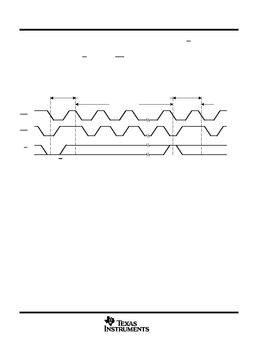
Test Mode Cycle
Entry Cycle
Exit Cycle
Normal
Mode
RAS
CAS
W
NOTE A: The states of W, data in, and address are defined by the type of cycle used during test mode.
Figure 1. Test-Mode Cycle
TMS416400, TMS416400P, TMS417400, TMS417400P
TMS426400, TMS426400P, TMS427400, TMS427400P
4194304-WORD BY 4-BIT HIGH-SPEED DRAMS
SMKS881B ≠ MAY 1995 ≠ REVISED AUGUST 1995
5
POST OFFICE BOX 1443
∑
HOUSTON, TEXAS 77251≠1443
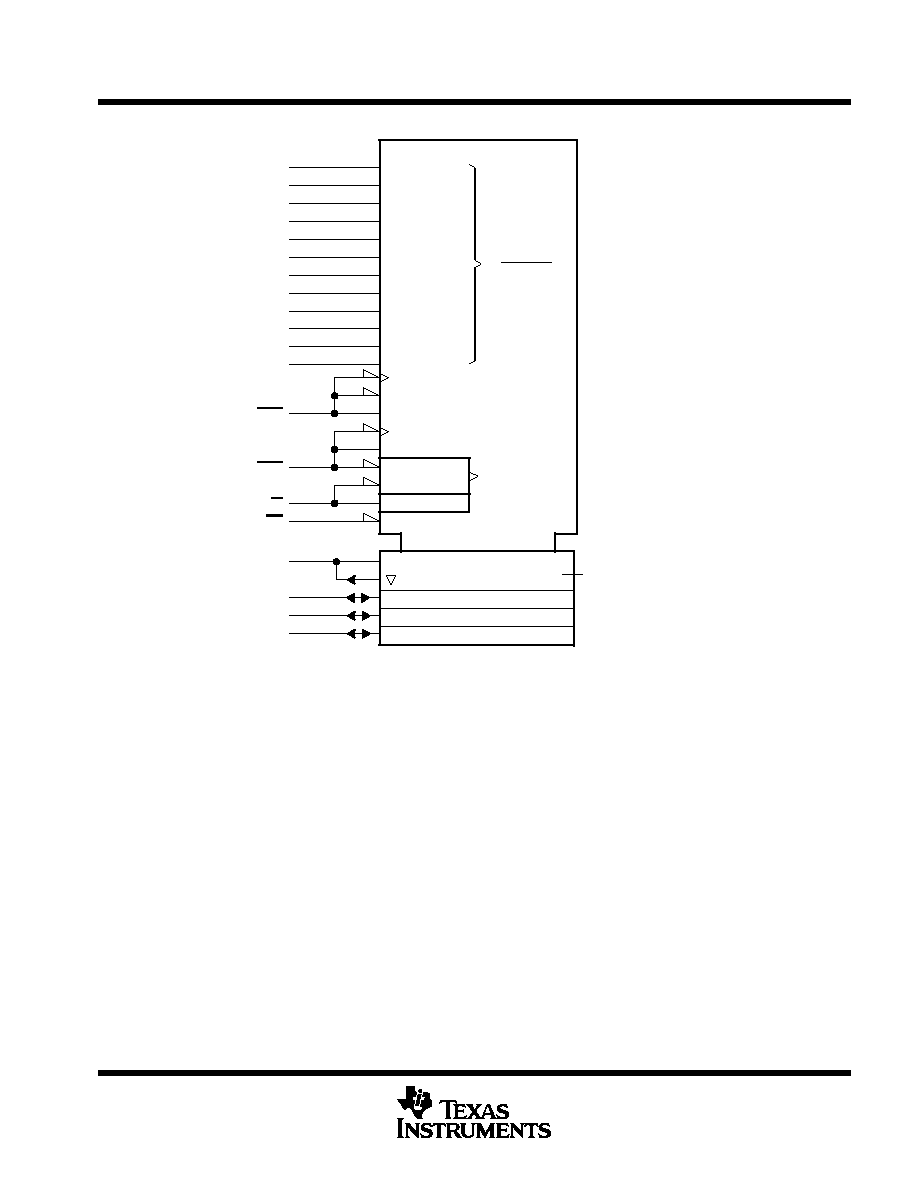
logic symbol
A0
A1
A2
A3
A4
A5
A6
A7
A8
RAS
CAS
W
OE
9
10
11
12
19
15
16
17
18
5
25
4
22
20D10/21D0
20D19/21D9
C20 [ROW]
G23/[REFRESH ROW]
24 [PWR DWN]
C21[COLUMN]
G24
23C22
23,21D
24,25 EN
G25
A
0
4 194 303
RAM 4096 K
◊
4
&
A9
21
2
3
24
25
A,Z26
A,22D
26
DQ1
DQ2
DQ3
DQ4
A10
8
20D21
A11
6
20D20
This symbol is in accordance with ANSI/IEEE Std 91-1984 and IEC Publication 647-12.
A11 is NC for TMS4x7400 and TMS4x7400P.