 | –≠–ª–µ–∫—Ç—Ä–æ–Ω–Ω—ã–π –∫–æ–º–ø–æ–Ω–µ–Ω—Ç: TPA0132 | –°–∫–∞—á–∞—Ç—å:  PDF PDF  ZIP ZIP |
TPA0132
2-W STEREO AUDIO POWER AMPLIFIER
WITH DC VOLUME CONTROL
SLOS223B ≠ MAY 1999 ≠ REVISED MARCH 2000
1
POST OFFICE BOX 655303
∑
DALLAS, TEXAS 75265
D
Compatible With PC 99 Desktop Line-Out
Into 10-k
Load
D
Compatible With PC 99 Portable Into 8-
Load
D
Internal Gain Control, Which Eliminates
External Gain-Setting Resistors
D
DC Volume Control From +20 dB to ≠40 dB
D
2-W/Ch Output Power Into 3-
Load
D
PC-Beep Input
D
Depop Circuitry
D
Stereo Input MUX
D
Fully Differential Input
D
Low Supply Current and Shutdown Current
D
Surface-Mount Power Packaging
24-Pin TSSOP PowerPAD
TM
description
The TPA0132 is a stereo audio power amplifier in a 24-pin TSSOP thermally enhanced package capable of
delivering 2 W of continuous RMS power per channel into 3-
loads. This device minimizes the number of
external components needed, which simplifies the design and frees up board space for other features. When
driving 1 W into 8-
speakers, the TPA0132 has less than 0.4% THD+N across its specified frequency range.
Included within this device is integrated depop circuitry that virtually eliminates transients that cause noise in
the speakers.
Amplifier gain is controlled by means of a dc voltage input on the VOLUME terminal. There are 31 discrete steps
covering the range of +20 dB (maximum volume setting) to ≠40 dB (minimum volume setting) in 2 dB steps.
When the VOLUME terminal exceeds 3.54 V, the device is muted. An internal input MUX allows two sets of
stereo inputs to the amplifier. In notebook applications, where internal speakers are driven as BTL and the line
outputs (often headphone drive) are required to be SE, the TPA0132 automatically switches into SE mode when
the SE/BTL input is activated, and this effectively reduces the gain by 6 dB.
The TPA0132 consumes only 10 mA of supply current during normal operation. A miserly shutdown mode is
included that reduces the supply current to less than 150
µ
A.
The PowerPAD package (PWP) delivers a level of thermal performance that was previously achievable only
in TO-220-type packages. Thermal impedances of approximately 35
∞
C/W are readily realized in multilayer PCB
applications. This allows the TPA0132 to operate at full power into 8-
loads at ambient temperatures of 85
∞
C.
Please be aware that an important notice concerning availability, standard warranty, and use in critical applications of
Texas Instruments semiconductor products and disclaimers thereto appears at the end of this data sheet.
Copyright
©
2000, Texas Instruments Incorporated
PRODUCTION DATA information is current as of publication date.
Products conform to specifications per the terms of Texas Instruments
standard warranty. Production processing does not necessarily include
testing of all parameters.
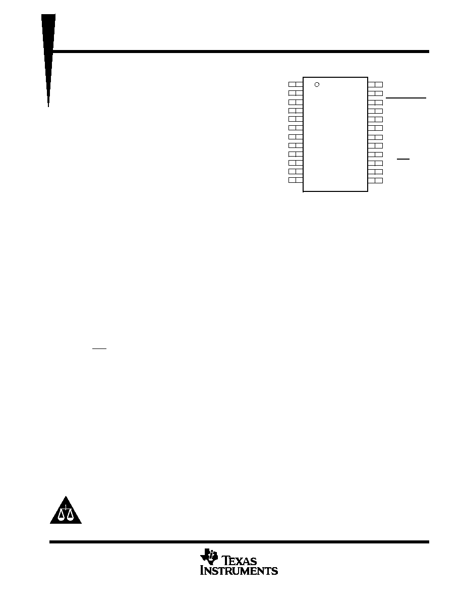
1
2
3
4
5
6
7
8
9
10
11
12
24
23
22
21
20
19
18
17
16
15
14
13
PWP PACKAGE
(TOP VIEW)
GND
PCB ENABLE
VOLUME
LOUT+
LLINEIN
LHPIN
PV
DD
RIN
LOUT≠
LIN
BYPASS
GND
GND
RLINEIN
SHUTDOWN
ROUT+
RHPIN
V
DD
PV
DD
CLK
ROUT≠
SE/BTL
PC-BEEP
GND
PowerPAD is a trademark of Texas Instruments Incorporated.
TPA0132
2-W STEREO AUDIO POWER AMPLIFIER
WITH DC VOLUME CONTROL
SLOS223B ≠ MAY 1999 ≠ REVISED MARCH 2000
2
POST OFFICE BOX 655303
∑
DALLAS, TEXAS 75265
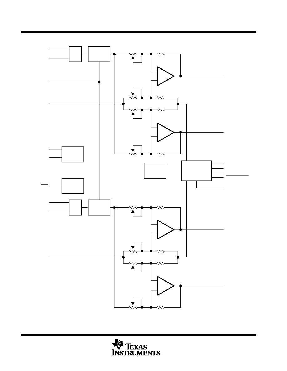
functional block diagram
ROUT+
≠
+
≠
+
R
MUX
32-Step
Volume
Control
PC
Beep
MUX
Control
Depop
Circuitry
Power
Management
≠
+
≠
+
L
MUX
32-Step
Volume
Control
RHPIN
RLINEIN
VOLUME
RIN
PC-BEEP
SE/BTL
LHPIN
LLINEIN
LIN
ROUT≠
PVDD
VDD
BYPASS
SHUTDOWN
GND
LOUT+
LOUT≠
PCB ENABLE

TPA0132
2-W STEREO AUDIO POWER AMPLIFIER
WITH DC VOLUME CONTROL
SLOS223B ≠ MAY 1999 ≠ REVISED MARCH 2000
3
POST OFFICE BOX 655303
∑
DALLAS, TEXAS 75265
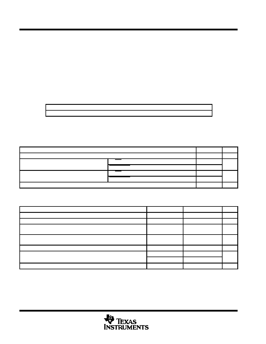
AVAILABLE OPTIONS
PACKAGED DEVICE
TA
TSSOP
(PWP)
≠ 40
∞
C to 85
∞
C
TPA0132PWP
The PWP package is available taped and reeled. To order a taped and reeled part,
add the suffix R to the part number (e.g., TPA0132PWPR).
Terminal Functions
TERMINAL
I/O
DESCRIPTION
NAME
NO.
I/O
DESCRIPTION
BYPASS
11
Tap to voltage divider for internal mid-supply bias generator
CLK
17
I
If a 47-nF capacitor is attached, the TPA0132 generates an internal clock. An external clock can override
the internal clock input to this terminal.
GND
1, 12
13, 24
Ground connection for circuitry. Connected to thermal pad.
LHPIN
6
I
Left channel headphone input, selected when SE/BTL is held high
LIN
10
I
Common left input for fully differential input. AC ground for single-ended inputs.
LLINEIN
5
I
Left channel line negative input, selected when SE/BTL is held low
LOUT+
4
O
Left channel positive output in BTL mode and positive output in SE mode
LOUT≠
9
O
Left channel negative output in BTL mode and high-impedance in SE mode
PCB ENABLE
2
I
If this terminal is high, the detection circuitry for PC-BEEP is overridden and passes PC-BEEP through
the amplifier, regardless of its amplitude. If PCB ENABLE is floating or low, the amplifier continues to
operate normally.
PC-BEEP
14
I
The input for PC Beep mode. PC-BEEP is enabled when a > 1-V (peak-to-peak) square wave is input
to PC-BEEP or PCB ENABLE is high.
PVDD
7, 18
I
Power supply for output stage
RHPIN
20
I
Right channel headphone input, selected when SE/BTL is held high
RIN
8
I
Common right input for fully differential input. AC ground for single-ended inputs.
RLINEIN
23
I
Right channel line input, selected when SE/BTL is held low
ROUT+
21
O
Right channel positive output in BTL mode and positive output in SE mode
ROUT≠
16
O
Right channel negative output in BTL mode and high-impedance in SE mode
SE/BTL
15
I
Input MUX control input. When this terminal is held high, the LHPIN or RHPIN and SE output is selected.
When this terminal is held low, the LLINEIN or RLINEIN and BTL output are selected.
SHUTDOWN
22
I
When held low, this terminal places the entire device, except PC-BEEP detect circuitry, in shutdown
mode.
VDD
19
I
Analog VDD input supply. This terminal needs to be isolated from PVDD to achieve highest performance.
VOLUME
3
I
VOLUME detects the dc level at the terminal and sets the gain for 31 discrete steps covering a range of
20 dB to ≠40 dB for dc levels of 0.15 V to 3.54. When the dc level is over 3.54 V, the device is muted.
TPA0132
2-W STEREO AUDIO POWER AMPLIFIER
WITH DC VOLUME CONTROL
SLOS223B ≠ MAY 1999 ≠ REVISED MARCH 2000
4
POST OFFICE BOX 655303
∑
DALLAS, TEXAS 75265
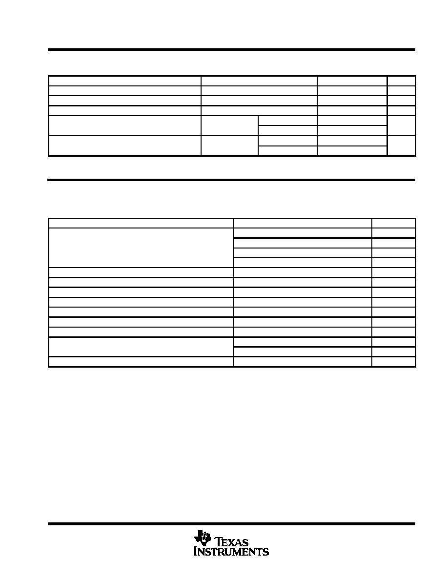
absolute maximum ratings over operating free-air temperature range (unless otherwise noted)
Supply voltage, V
DD
6 V
. . . . . . . . . . . . . . . . . . . . . . . . . . . . . . . . . . . . . . . . . . . . . . . . . . . . . . . . . . . . . . . . . . . . . . . .
Input voltage, V
I
≠0.3 V to V
DD
+0.3 V
. . . . . . . . . . . . . . . . . . . . . . . . . . . . . . . . . . . . . . . . . . . . . . . . . . . . . . . . . . . .
Continuous total power dissipation
internally limited (see Dissipation Rating Table)
. . . . . . . . . . . . . . . . . . . . .
Operating free-air temperature range, T
A
≠ 40
∞
C to 85
∞
C
. . . . . . . . . . . . . . . . . . . . . . . . . . . . . . . . . . . . . . . . . . . .
Operating junction temperature range, T
J
≠ 40
∞
C to 150
∞
C
. . . . . . . . . . . . . . . . . . . . . . . . . . . . . . . . . . . . . . . . . . .
Storage temperature range, T
stg
≠65
∞
C to 150
∞
C
. . . . . . . . . . . . . . . . . . . . . . . . . . . . . . . . . . . . . . . . . . . . . . . . . . .
Lead temperature 1,6 mm (1/16 inch) from case for 10 seconds
260
∞
C
. . . . . . . . . . . . . . . . . . . . . . . . . . . . . . .
Stresses beyond those listed under "absolute maximum ratings" may cause permanent damage to the device. These are stress ratings only, and
functional operation of the device at these or any other conditions beyond those indicated under "recommended operating conditions" is not
implied. Exposure to absolute-maximum-rated conditions for extended periods may affect device reliability.
DISSIPATION RATING TABLE
PACKAGE
TA
25
∞
C
DERATING FACTOR
TA = 70
∞
C
TA = 85
∞
C
PWP
2.7 Wß
21.8 mW/
∞
C
1.7 W
1.4 W
ß Please see the Texas Instruments document, PowerPAD Thermally Enhanced Package Application Report
(literature number SLMA002), for more information on the PowerPAD package. The thermal data was
measured on a PCB layout based on the information in the section entitled
Texas Instruments Recommended
Board for PowerPAD on page 33 of the before mentioned document.
recommended operating conditions
MIN
MAX
UNIT
¡¡¡¡¡¡¡¡¡¡¡¡¡¡¡¡¡¡¡¡¡¡¡¡¡¡¡¡
¡¡¡¡¡¡¡¡¡¡¡¡¡¡¡¡¡¡¡¡¡¡¡¡¡¡¡¡
Supply voltage, VDD
¡¡¡
¡¡¡
4.5
¡¡¡
¡¡¡
5.5
¡¡¡
¡¡¡
V
High level input voltage VIH
SE/BTL
4
V
High-level input voltage, VIH
SHUTDOWN
2
V
Low level input voltage VIL
SE/BTL
3
V
Low-level input voltage, VIL
SHUTDOWN
0.8
V
¡¡¡¡¡¡¡¡¡¡¡¡¡¡¡¡¡¡¡¡¡¡¡¡¡¡¡¡
¡¡¡¡¡¡¡¡¡¡¡¡¡¡¡¡¡¡¡¡¡¡¡¡¡¡¡¡
Operating free-air temperature, TA
¡¡¡
¡¡¡
≠ 40
¡¡¡
¡¡¡
85
¡¡¡
¡¡¡
∞
C
electrical characteristics at specified free-air temperature, V
DD
= 5 V, T
A
= 25
∞
C (unless otherwise
noted)
PARAMETER
TEST CONDITIONS
MIN
TYP
MAX
UNIT
¡¡¡¡
¡¡¡¡
|VOO|
¡¡¡¡¡¡¡¡¡¡¡¡¡¡¡¡¡
¡¡¡¡¡¡¡¡¡¡¡¡¡¡¡¡¡
Output offset voltage (measured differentially)
¡¡¡¡¡¡¡
¡¡¡¡¡¡¡
VI = 0, AV = 2
¡¡¡
¡¡¡
¡¡¡
¡¡¡
¡¡¡
¡¡¡
25
¡¡¡
¡¡¡
mV
¡¡¡¡
¡¡¡¡
PSRR
¡¡¡¡¡¡¡¡¡¡¡¡¡¡¡¡¡
¡¡¡¡¡¡¡¡¡¡¡¡¡¡¡¡¡
Power supply rejection ratio
¡¡¡¡¡¡¡
¡¡¡¡¡¡¡
VDD = 4 V to 5 V
¡¡¡
¡¡¡
¡¡¡
¡¡¡
67
¡¡¡
¡¡¡
¡¡¡
¡¡¡
dB
|IIH|
High-level input current
VDD = 5.5 V,
VI = VDD
¡¡¡
¡
¡
¡
¡¡¡
¡¡¡
¡
¡
¡
¡¡¡
¡¡¡
¡
¡
¡
¡¡¡
900
¡¡¡
¡
¡
¡
¡¡¡
nA
|IIL|
Low-level input current
VDD = 5.5 V,
VI = 0 V
¡¡¡
¡¡¡
¡¡¡
¡¡¡
¡¡¡
¡¡¡
900
¡¡¡
¡¡¡
nA
ZI
Input impedance
¡¡¡¡¡¡¡
¡¡¡¡¡¡¡
See Figure 28
¡¡¡
¡¡¡
¡¡¡¡
¡¡¡¡
IDD
¡¡¡¡¡¡¡¡¡¡¡¡¡¡¡¡¡
¡¡¡¡¡¡¡¡¡¡¡¡¡¡¡¡¡
Supply current
¡¡¡¡¡¡¡
¡¡¡¡¡¡¡
BTL mode
¡¡¡
¡¡¡
¡¡¡
¡¡¡
10
¡¡¡
¡¡¡
15
¡¡¡
¡¡¡
mA
¡¡¡¡
¡¡¡¡
IDD
¡¡¡¡¡¡¡¡¡¡¡¡¡¡¡¡¡
¡¡¡¡¡¡¡¡¡¡¡¡¡¡¡¡¡
Supply current
¡¡¡¡¡¡¡
¡¡¡¡¡¡¡
SE mode
¡¡¡
¡¡¡
¡¡¡
¡¡¡
5
¡¡¡
¡¡¡
7.5
¡¡¡
¡¡¡
mA
¡¡¡¡
¡¡¡¡
IDD(SD)
¡¡¡¡¡¡¡¡¡¡¡¡¡¡¡¡¡
¡¡¡¡¡¡¡¡¡¡¡¡¡¡¡¡¡
Supply current, shutdown mode
¡¡¡¡¡¡¡
¡¡¡¡¡¡¡
¡¡¡
¡¡¡
¡¡¡
¡¡¡
150
¡¡¡
¡¡¡
300
¡¡¡
¡¡¡
µ
A
TPA0132
2-W STEREO AUDIO POWER AMPLIFIER
WITH DC VOLUME CONTROL
SLOS223B ≠ MAY 1999 ≠ REVISED MARCH 2000
5
POST OFFICE BOX 655303
∑
DALLAS, TEXAS 75265
operating characteristics, V
DD
= 5 V, T
A
= 25
∞
C, R
L
= 4
, Gain = 2 V/V, BTL mode (unless otherwise
noted)
PARAMETER
TEST CONDITIONS
MIN
TYP
MAX
UNIT
¡¡¡¡
¡¡¡¡
PO
¡¡¡¡¡¡¡¡¡¡¡
¡¡¡¡¡¡¡¡¡¡¡
Output power
¡¡¡¡¡¡
¡¡¡¡¡¡
THD = 1%,
¡¡¡¡¡¡¡
¡¡¡¡¡¡¡
f = 1 kHz
¡¡¡
¡¡¡
¡¡¡
¡¡¡
2
¡¡¡
¡¡¡
¡¡¡
¡¡¡
W
¡¡¡¡
¡¡¡¡
THD + N
¡¡¡¡¡¡¡¡¡¡¡
¡¡¡¡¡¡¡¡¡¡¡
Total harmonic distortion plus noise
¡¡¡¡¡¡
¡¡¡¡¡¡
PO = 1 W,
¡¡¡¡¡¡¡
¡¡¡¡¡¡¡
f = 20 Hz to 15 kHz
¡¡¡
¡¡¡
¡¡¡
¡¡¡
0.4%
¡¡¡
¡¡¡
¡¡¡
¡¡¡
¡¡¡¡
¡¡¡¡
BOM
¡¡¡¡¡¡¡¡¡¡¡
¡¡¡¡¡¡¡¡¡¡¡
Maximum output power bandwidth
¡¡¡¡¡¡
¡¡¡¡¡¡
THD = 5%
¡¡¡¡¡¡¡
¡¡¡¡¡¡¡
¡¡¡
¡¡¡
¡¡¡
¡¡¡
>15
¡¡¡
¡¡¡
¡¡¡
¡¡¡
kHz
¡¡¡¡
¡¡¡¡
¡¡¡¡¡¡¡¡¡¡¡
¡¡¡¡¡¡¡¡¡¡¡
Supply ripple rejection ratio
¡¡¡¡¡¡
¡¡¡¡¡¡
f = 1 kHz,
¡¡¡¡¡¡¡
¡¡¡¡¡¡¡
BTL mode
¡¡¡
¡¡¡
¡¡¡
¡¡¡
65
¡¡¡
¡¡¡
¡¡¡
¡¡¡
dB
¡¡¡¡
¡¡¡¡
¡¡¡¡¡¡¡¡¡¡¡
¡¡¡¡¡¡¡¡¡¡¡
Supply ripple rejection ratio
¡¡¡¡¡¡
¡¡¡¡¡¡
,
CB = 0.47
µ
F
¡¡¡¡¡¡¡
¡¡¡¡¡¡¡
SE mode
¡¡¡
¡¡¡
¡¡¡
¡¡¡
60
¡¡¡
¡¡¡
¡¡¡
¡¡¡
dB
¡¡¡¡
V
¡¡¡¡¡¡¡¡¡¡¡
Noise output voltage
¡¡¡¡¡¡
CB = 0.47
µ
F,
¡¡¡¡¡¡¡
BTL mode
¡¡¡
¡¡¡
34
¡¡¡
¡¡¡
µ
VRMS
¡¡¡¡
¡¡¡¡
Vn
¡¡¡¡¡¡¡¡¡¡¡
¡¡¡¡¡¡¡¡¡¡¡
Noise output voltage
¡¡¡¡¡¡
¡¡¡¡¡¡
B
µ
f = 20 Hz to 20 kHz
¡¡¡¡¡¡¡
¡¡¡¡¡¡¡
SE mode
¡¡¡
¡¡¡
¡¡¡
¡¡¡
44
¡¡¡
¡¡¡
¡¡¡
¡¡¡
µ
VRMS
TYPICAL CHARACTERISTICS
Table of Graphs
FIGURE
vs Output power
1, 4, 6, 8, 10
THD+N
Total harmonic distortion plus noise
vs Gain
2
THD+N
Total harmonic distortion plus noise
vs Frequency
3, 5, 7, 9, 11
vs Output voltage
12
Vn
Output noise voltage
vs Frequency
13
Supply ripple rejection ratio
vs Frequency
14, 15
Crosstalk
vs Frequency
16, 17, 18
Shutdown attenuation
vs Frequency
19
SNR
Signal-to-noise ratio
vs Frequency
20
Closed loop response
21, 22
PO
Output power
vs Load resistance
23, 24
PD
Power dissipation
vs Output power
25, 26
PD
Power dissipation
vs Ambient temperature
27
ZI
Input impedance
vs Gain
28