 | –≠–ª–µ–∫—Ç—Ä–æ–Ω–Ω—ã–π –∫–æ–º–ø–æ–Ω–µ–Ω—Ç: TPA032D03 | –°–∫–∞—á–∞—Ç—å:  PDF PDF  ZIP ZIP |
TPA032D03
10-W MONO CLASS-D AUDIO POWER AMPLIFIER
SLOS283A ≠ DECEMBER 1999 ≠ REVISED MARCH 2000
1
POST OFFICE BOX 655303
∑
DALLAS, TEXAS 75265
D
Extremely Efficient Class-D Mono
Operation
D
Drives Mono Speaker, Plus Stereo
Headphones
D
10-W BTL Output Into 4
From 12 V
D
32-W Peak Music Power
D
Fully Specified for 12-V Operation
D
Low Shutdown Current
D
Class-AB Headphone Amplifier
D
Thermally-Enhanced PowerPAD
TM
Surface-
Mount Packaging
D
Thermal and Under-Voltage Protection
description
The TPA032D03 is a monolithic power IC mono
audio amplifier that operates in extremely efficient
Class-D operation, using the high switching speed
of power DMOS transistors to replicate the analog
input signal through high-frequency switching of
the output stage. This allows the TPA032D03 to
be configured as a bridge-tied load (BTL) amplifier
capable of delivering up to 10 W of continuous
average power into a 4-
load at 0.5% THD+N
from a 12-V power supply in the high-fidelity audio
frequency range (20 Hz to 20 kHz). A BTL
configuration eliminates the need for external
coupling capacitors on the output. Included is a Class-AB headphone amplifier with interface logic to select
between the two modes of operation. Only one amplifier is active at any given time, and the other is in
power-saving sleep mode. Also, a chip-level shutdown control is provided to limit total supply current to 20
µ
A,
making the device ideal for battery-powered applications.
The output stage is compatible with a range of power supplies from 8 V to 14 V. Protection circuitry is included
to increase device reliability: thermal and under-voltage shutdown, with a status feedback terminal for use when
any error condition is encountered.
The high switching frequency of the TPA032D03 allows the output filter to consist of three small capacitors and
two small inductors per channel. The high switching frequency also allows for good THD+N performance.
The TPA032D03 is offered in the thermally enhanced 48-pin PowerPAD TSSOP surface-mount package
(designator DCA).
Copyright
©
2000, Texas Instruments Incorporated
PRODUCTION DATA information is current as of publication date.
Products conform to specifications per the terms of Texas Instruments
standard warranty. Production processing does not necessarily include
testing of all parameters.
Please be aware that an important notice concerning availability, standard warranty, and use in critical applications of
Texas Instruments semiconductor products and disclaimers thereto appears at the end of this data sheet.
PowerPAD is a trademark of Texas Instruments Incorporated.
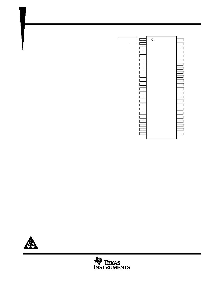
SHUTDOWN
MUTE
MODE
INN
INP
COMP
AGND
V
DD
PV
DD
OUTP
OUTP
PGND
PGND
OUTN
OUTN
PV
DD
HPREG
HPLOUT
HPLIN
AGND
PV
DD
VCP
HPDL
CP1
COSC
AGND
AGND
AGND
AGND
AGND
FAULT0
FAULT1
PV
DD
NC
NC
PGND
PGND
NC
NC
PV
DD
HPV
CC
HPROUT
HPRIN
V2P5
PV
DD
PGND
HPDR
CP2
NC ≠ No internal connection
1
2
3
4
5
6
7
8
9
10
11
12
13
14
15
16
17
18
19
20
21
22
23
24
48
47
46
45
44
43
42
41
40
39
38
37
36
35
34
33
32
31
30
29
28
27
26
25
DCA PACKAGE
(TOP VIEW)
TP
A032D03
10-W MONO CLASS-D
AUDIO POWER
AMPLIFIER
SLOS283A
≠ DECEMBER 1999 ≠ REVISED MARCH 2000
T
emp
l
ate
R
e
l
ease
D
ate:
7
≠
11
≠
94
2
POST
OFFICE BOX 655303 DALLAS,
TEXAS
75265
∑
_
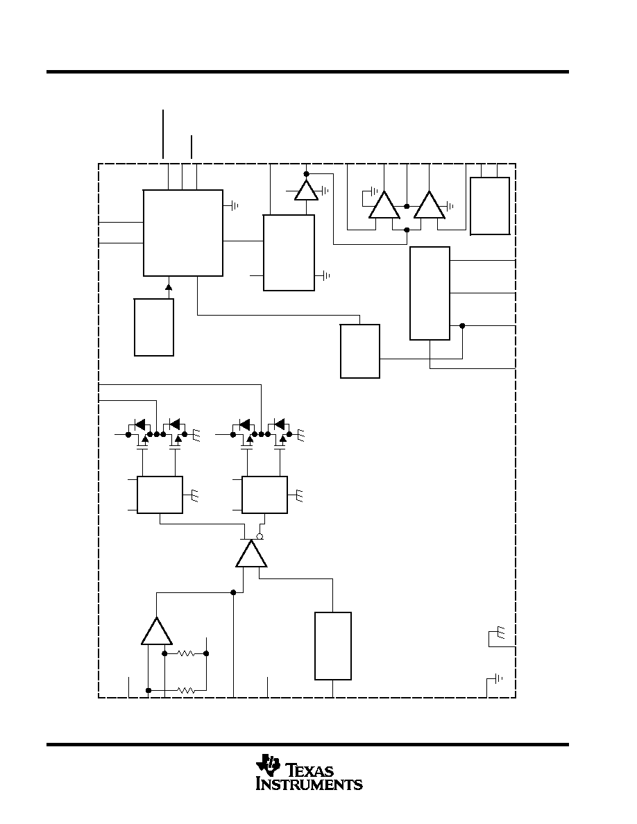
+
_
+
INP
RAMP
GENERATOR
GATE
DRIVE
PVDD
GATE
DRIVE
PVDD
THERMAL
DETECT
VCP-UVLO
DETECT
DOUBLER
CHARGE PUMP
_
+
_
+
CONTROL and
STARTUP
LOGIC
5-V
REGULATOR
and BIASES
HPVCC
PVDD
INN
COMP
COSC
PVDD
PV
DD
VCP
CP2
CP1
OUTP
OUTN
F
AUL
T0
F
AUL
T1
SHUTDOWN
MODE
MUTE
HPREG
V2P5
HPLIN
HPLOUT
HPVCC
HPROUT
HPRIN
LPVDD
PGND
VCP
PVDD
VCP
PVDD
VDD
VDD
10 k
10 k
1.5 V
HP
DEPOP
HPDL
HPDR
AGND
NOTE A: VDD and PVDD are externally connected. AGND and PGND are externally connected.
schematic
TPA032D03
10-W MONO CLASS-D AUDIO POWER AMPLIFIER
SLOS283A ≠ DECEMBER 1999 ≠ REVISED MARCH 2000
3
POST OFFICE BOX 655303
∑
DALLAS, TEXAS 75265
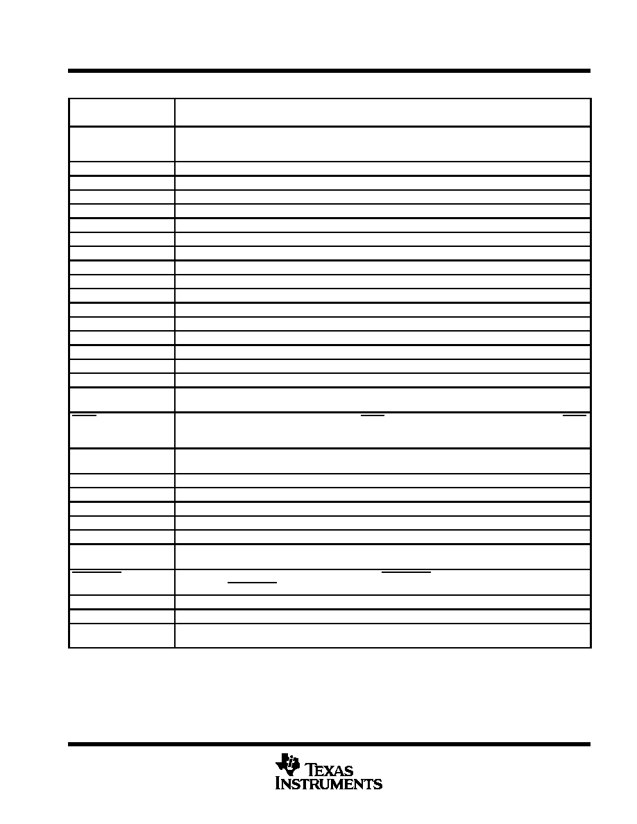
Terminal Functions
TERMINAL
DESCRIPTION
NAME
NO.
DESCRIPTION
AGND
7, 20,
43, 44,
45, 46, 47
Analog ground for headphone and Class-D analog sections
COMP
6
Compensation capacitor terminal for Class-D amplifier
COSC
48
Connect a capacitor from analog ground to this terminal to set the frequency of the ramp reference signal.
CP1
24
First diode node for charge pump
CP2
25
First inverter switching node for charge pump
FAULT0
42
Logic level fault0 output signal. Lower order bit of the two fault signals with open drain output.
FAULT1
41
Logic level fault1 output signal. Higher order bit of the two fault signals with open drain output.
HPDL
23
Depop control for left headphone
HPDR
26
Depop control for right headphone
HPLIN
19
Headphone amplifier left input
HPLOUT
18
Headphone amplifier left output
HPREG
17
5-V regulator output. This terminal requires a 1-
µ
F capacitor to ground for stability reasons.
HPRIN
30
Headphone amplifier right input
HPROUT
31
Headphone amplifier right output
HPVCC
32
5V supply to headphone amplifier and logic. This terminal is typically connected to HPREG.
INN
4
Class-D negative input
INP
5
Class-D positive input
MODE
3
TTL logic-level mode input signal. When MODE is held low, the main Class-D amplifier is active. When MODE is
held > high, the head phone amplifier is active.
MUTE
2
Active-low TTL logic-level mute input signal. When MUTE is held low, the selected amplifier is muted. When MUTE
is held > high, the device operates normally. When the Class-D amplifier is muted, the low-side output transistors
are turned on, shorting the load to ground.
NC
34, 35,
38, 39
No connection
OUTN
14, 15
Class-D amplifier negative output of H-bridge
OUTP
10, 11
Class-D amplifier positive output of H-bridge
PGND
12, 13
Power ground for H≠bridge only
PGND
27
Power ground for charge pump only
PGND
36, 37
Power ground for H-bridge only
PVDD
9, 16, 21,
28, 33, 40
VDD supply for charge-pump, headphone regulator, Class-D amplifier, and gate drive circuitry
SHUTDOWN
1
Active-low TTL logic-level shutdown input signal. When SHUTDOWN is held low, the device goes into shutdown
mode. When SHUTDOWN is held high, the device operates normally.
V2P5
29
2.5V internal reference bypass. This terminal requires a capacitor to ground.
VCP
22
Connect a capacitor from this terminal to power ground to provide storage for the charge pump output voltage.
VDD
8
VDD bias supply for analog circuitry. This terminal needs to be well filtered to prevent degrading the device
performance.
TPA032D03
10-W MONO CLASS-D AUDIO POWER AMPLIFIER
SLOS283A ≠ DECEMBER 1999 ≠ REVISED MARCH 2000
4
POST OFFICE BOX 655303
∑
DALLAS, TEXAS 75265
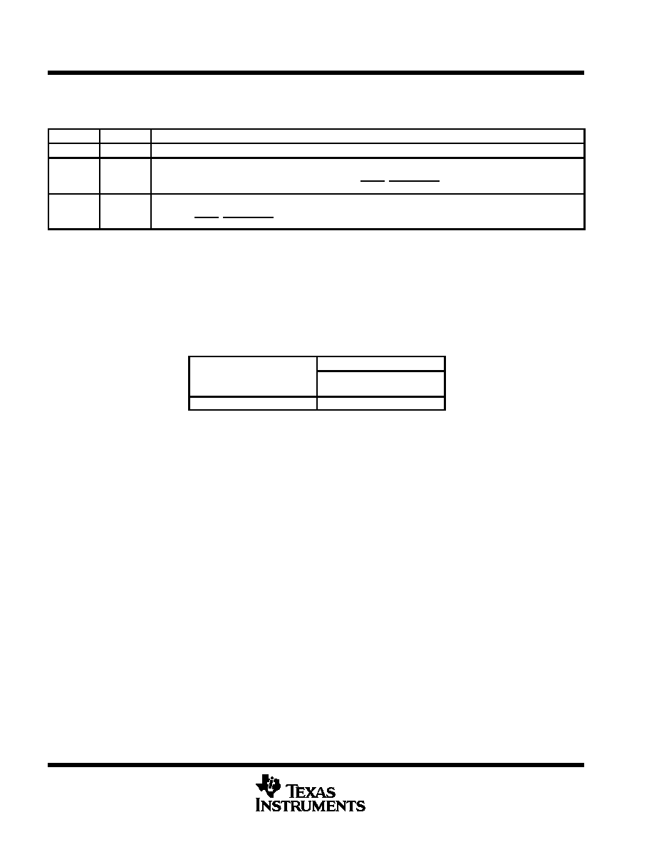
Class-D amplifier faults
Table 1. Class-D Amplifier Fault Table
FAULT 0
FAULT 1
DESCRIPTION
1
1
No fault. The device is operating normally.
0
1
Charge pump under-voltage lock-out (VCP-UV) fault. All low-side transistors are turned on, shorting the load to
ground. Once the charge pump voltage is restored, normal operation resumes, but FAULT1 is still active. This is not
a latched fault, however. FAULT1 is cleared by cycling MUTE, SHUTDOWN, or the power supply.
0
0
Thermal fault. All the low-side transistors are turned on, shorting the load to ground. Once the junction temperature
drops 20
∞
C, normal operation resumes (not a latched fault). But the FAULTx terminals are still set and are cleared
by cycling MUTE, SHUTDOWN, or the power supply.
headphone amplifier faults
The thermal fault remains active when the device is in head phone mode. This fault operation has exactly the
same as it does for the Class-D amplifier (see Table 1).
If HPV
CC
drops below approximately 4.5 V, the head phone is disabled. Once HPV
CC
exceeds approximately
4.5 V, the head phone amplifier is re-enabled. No fault is reported to the user.
AVAILABLE OPTIONS
PACKAGED DEVICES
TA
TSSOP
(DCA)
≠ 40
∞
C to 125
∞
C
TPA032D03DCA
The DCA package is available in left-ended tape and reel. To order
a taped and reeled part, add the suffix R to the part number (e.g.,
TPA032D03DCAR).
TPA032D03
10-W MONO CLASS-D AUDIO POWER AMPLIFIER
SLOS283A ≠ DECEMBER 1999 ≠ REVISED MARCH 2000
5
POST OFFICE BOX 655303
∑
DALLAS, TEXAS 75265
absolute maximum ratings over operating free-air temperature range, T
C
= 25
∞
C (unless otherwise
noted)
Supply voltage, (V
DD
, PV
DD
)
14 V
. . . . . . . . . . . . . . . . . . . . . . . . . . . . . . . . . . . . . . . . . . . . . . . . . . . . . . . . . . . . . . . .
Headphone supply voltage, (HPV
CC
) 5.5
V
. . . . . . . . . . . . . . . . . . . . . . . . . . . . . . . . . . . . . . . . . . . . . . . . . . . . . . . .
Input voltage, V
I
(MUTE, MODE, SHUTDOWN)
≠ 0.3 V to 7 V
. . . . . . . . . . . . . . . . . . . . . . . . . . . . . . . . . . . . . . . .
Output current, I
O
(FAULT0, FAULT1), open drain terminated
1 mA
. . . . . . . . . . . . . . . . . . . . . . . . . . . . . . . . . . .
Supply/load voltage, (FAULT0, FAULT1)
7 V
. . . . . . . . . . . . . . . . . . . . . . . . . . . . . . . . . . . . . . . . . . . . . . . . . . . . . . .
Charge pump voltage, V
CP
PV
DD
+ 20 V
. . . . . . . . . . . . . . . . . . . . . . . . . . . . . . . . . . . . . . . . . . . . . . . . . . . . . . . . . .
Continuous H-bridge output current (1 H-bridge conducting)
3.5 A
. . . . . . . . . . . . . . . . . . . . . . . . . . . . . . . . . . . .
Pulsed H-Bridge output current, each output, I
max
(see Note 1)
7 A
. . . . . . . . . . . . . . . . . . . . . . . . . . . . . . . . . . .
Continuous HPREG output current, I
O
(HPREG)
150 mA
. . . . . . . . . . . . . . . . . . . . . . . . . . . . . . . . . . . . . . . . . . . .
Continuous total power dissipation, T
C
= 25
∞
C
See Dissipation Rating Table
. . . . . . . . . . . . . . . . . . . . . . . . . . .
Operating virtual junction temperature range, T
J
≠ 40
∞
C to 150
∞
C
. . . . . . . . . . . . . . . . . . . . . . . . . . . . . . . . . . . . .
Operating case temperature range, T
C
≠ 40
∞
C to 125
∞
C
. . . . . . . . . . . . . . . . . . . . . . . . . . . . . . . . . . . . . . . . . . . . .
Storage temperature range, T
stg
≠ 65
∞
C to 260
∞
C
. . . . . . . . . . . . . . . . . . . . . . . . . . . . . . . . . . . . . . . . . . . . . . . . . . .
Lead temperature 1,6 mm (1/16 inch) from case for 10 seconds
260
∞
C
. . . . . . . . . . . . . . . . . . . . . . . . . . . . . . .
Stresses beyond those listed under "absolute maximum ratings" may cause permanent damage to the device. These are stress ratings only, and
functional operation of the device at these or any other conditions beyond those indicated under "recommended operating conditions" is not
implied. Exposure to absolute-maximum-rated conditions for extended periods may affect device reliability.
NOTE 1: Pulse duration = 10 ms, duty cycle
v
2%
DISSIPATION RATING TABLE
PACKAGE
TA
25
∞
C
POWER RATING
DERATING FACTOR
ABOVE TA = 25
∞
C
TA = 70
∞
C
POWER RATING
TA = 85
∞
C
POWER RATING
DCA
5.6 W
44.8 mW/
∞
C
3.6 W
2.9 W
Please see the Texas Instruments document, PowerPAD Thermally Enhanced Package Application
Report (literature number SLMA002), for more information on the PowerPAD package. The thermal data
was measured on a PCB layout based on the information in the section entitled
Texas Instruments
Recommended Board for PowerPAD on page 33 of the before mentioned document.
recommended operating conditions
MIN
NOM
MAX
UNIT
Supply voltage, VDD, PVDD
8
14
V
Headphone supply voltage, HPVCC
4.5
5.5
V
High-level input voltage, VIH (MUTE, MODE, SHUTDOWN)
2
VDD + 0.3 V
V
Low-level input voltage, VIL (MUTE, MODE, SHUTDOWN)
≠ 0.3
0.8
V
Audio inputs, LINN, LINP, RINN, RINP, HPLIN, HPRIN, differential input voltage
1
VRMS
PWM frequency
100
250
500
kHZ