 | –≠–ª–µ–∫—Ç—Ä–æ–Ω–Ω—ã–π –∫–æ–º–ø–æ–Ω–µ–Ω—Ç: TPA2010D1 | –°–∫–∞—á–∞—Ç—å:  PDF PDF  ZIP ZIP |
TPA2010D1
SLOS417A - OCTOBER 2003 - REVISED DECEMBER 2003
2.5 W MONO FILTER FREE CLASS D AUDIO POWER AMPLIFIER
FEATURES
D
Maximum Battery Life and Minimum Heat
- Efficiency With an 8-
Speaker:
- 88% at 400 mW
- 80% at 100 mW
- 2.8-mA Quiescent Current
- 0.5-
µ
A Shutdown Current
D
Only Three External Components
- Optimized PWM Output Stage Eliminates
LC Output Filter
- Internally Generated 250-kHz Switching
Frequency Eliminates Capacitor and
Resistor
- Improved PSRR (-75 dB) and Wide Supply
Voltage (2.5 V to 5.5 V) Eliminates Need
for a Voltage Regulator
- Fully Differential Design Reduces RF
Rectification and Eliminates Bypass
Capacitor
- Improved CMRR Eliminates Two Input
Coupling Capacitors
D
Wafer Chip Scale Packaging (WCSP)
- NanoFree
E
Lead-Free (YZF)
- NanoStar
E
SnPb (YEF)
APPLICATIONS
D
Ideal for Wireless or Cellular Handsets and
PDAs
DESCRIPTION
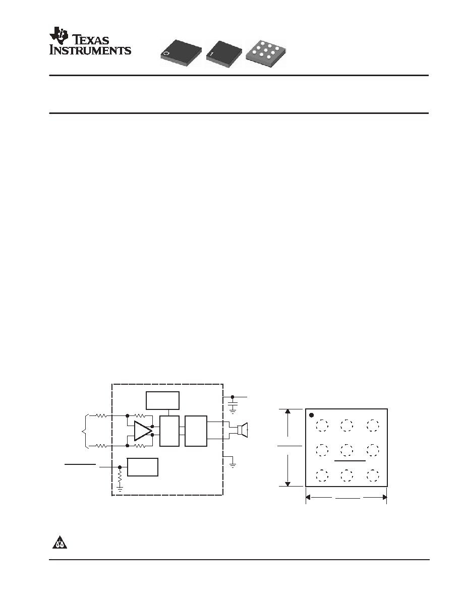
The TPA2010D1 is a 2.5-W high efficiency filter-free
class-D audio power amplifier in a 1.45 mm
◊
1.45 mm
wafer chip scale package (WCSP) that requires only three
external components.
Features like 88% efficiency, -75-dB PSRR, improved
RF-rectification immunity, and 8 mm
2
total PCB area make
the TPA2010D1 ideal for cellular handsets. A fast start-up
time of 1 ms with minimal pop makes the TP2010D1 ideal
for PDA applications.
In cellular handsets, the earpiece, speaker phone, and
melody ringer can each be driven by the TPA2010D1. The
TPA2010D1 allows independent gain while summing
signals from seperate sources, and has a low 36
µ
V noise
floor, A-weighted.
APPLICATION CIRCUIT
_
+
IN-
IN+
PWM
H-
Bridge
VO+
VO-
Internal
Oscillator
CS
To Battery
VDD
GND
Bias
Circuitry
RI
RI
+
-
Differential
Input
TPA2010D1
SHUTDOWN
A1
A2
A3
B1
B2
B3
C1
C2
C3
IN+
GND
VO-
VDD
PVDD
GND
IN-
SHUTDOWN VO+
1,55 mm
9-BALL
WAFER CHIP SCALE
YZF, YEF PACKAGES
TPA2010D1 DIMENSIONS
(TOP VIEW OF PCB)
Note: Pin A1 is marked with a "0" for
Pb-free (YZF) and a "1" for SnPb (YEF).
1,40 mm
1,55 mm
1,40 mm
PRODUCTION DATA information is current as of publication date. Products
conform to specifications per the terms of Texas Instruments standard warranty.
Production processing does not necessarily include testing of all parameters.
Please be aware that an important notice concerning availability, standard warranty, and use in critical applications of Texas Instruments
semiconductor products and disclaimers thereto appears at the end of this data sheet.
www.ti.com
Copyright
2003, Texas Instruments Incorporated
NanoFree and NanoStar are trademarks of Texas Instruments.
TPA2010D1
SLOS417A - OCTOBER 2003 - REVISED DECEMBER 2003
www.ti.com
2
This integrated circuit can be damaged by ESD. Texas Instruments recommends that all integrated circuits be handled with appropriate
precautions. Failure to observe proper handling and installation procedures can cause damage.
ORDERING INFORMATION
TA
PACKAGE
PART NUMBER
SYMBOL
-40
∞
C to 85
∞
C
Wafer chip scale package (YEF)
TPA2010D1YEF (1)
AJZ
-40
∞
C to 85
∞
C
Wafer chip scale packaging - Lead free (YZF)
TPA2010D1YZF (1)
AKO
(1) The YEF and YZF packages are only available taped and reeled. To order add the suffix "R" to the end of the part number for a reel of 3000, or
add the suffix "T" to the end of the part number for a reel of 250 (e.g. TPA2010D1YEFR).
ABSOLUTE MAXIMUM RATINGS
over operating free-air temperature range unless otherwise noted(1)
TPA2010D1
Supply voltage, VDD
In active mode
-0.3 V to 6 V
Supply voltage, VDD
In SHUTDOWN mode
-0.3 V to 7 V
Input voltage, VI
-0.3 V to VDD + 0.3 V
Continuous total power dissipation
See Dissipation Rating Table
Operating free-air temperature, TA
-40
∞
C to 85
∞
C
Operating junction temperature, TJ
-40
∞
C to 125
∞
C
Storage temperature, Tstg
-65
∞
C to 150
∞
C
Lead temperature 1,6 mm (1/16 inch) from case for 10 seconds
YZF
260
∞
C
Lead temperature 1,6 mm (1/16 inch) from case for 10 seconds
YEF
235
∞
C
(1) Stresses beyond those listed under "absolute maximum ratings" may cause permanent damage to the device. These are stress ratings only, and
functional operation of the device at these or any other conditions beyond those indicated under "recommended operating conditions" is not
implied. Exposure to absolute-maximum-rated conditions for extended periods may affect device reliability.
RECOMMENDED OPERATING CONDITIONS
MIN
NOM
MAX
UNIT
Supply voltage, VDD
2.5
5.5
V
High-level input voltage, VIH
SHUTDOWN
1.3
VDD
V
Low-level input voltage, VIL
SHUTDOWN
0
0.35
V
Input resistor, RI
Gain
20 V/V (26 dB)
15
k
Common mode input voltage range, VIC
VDD = 2.5 V, 5.5 V, CMRR
-49 dB
0.5
VDD-0.8
V
Operating free-air temperature, T
A
-40
85
∞
C
PACKAGE DISSIPATION RATINGS
PACKAGE
DERATING
FACTOR(1)
TA
25
∞
C
POWER RATING
TA = 70
∞
C
POWER RATING
TA = 85
∞
C
POWER RATING
YEF
7.8 mW/
∞
C
780 mW
429 mW
312 mW
YZF
7.8 mW/
∞
C
780 mW
429 mW
312 mW
(1) Derating factor measure with High K board.

TPA2010D1
SLOS417A - OCTOBER 2003 - REVISED DECEMBER 2003
www.ti.com
3
ELECTRICAL CHARACTERISTICS
TA = 25
∞
C (unless otherwise noted)
PARAMETER
TEST CONDITIONS
MIN
TYP
MAX
UNIT
|VOS|
Output offset voltage (measured
differentially)
VI = 0 V, AV = 2 V/V, VDD = 2.5 V to 5.5 V
1
25
mV
PSRR
Power supply rejection ratio
VDD = 2.5 V to 5.5 V
-75
-55
dB
CMRR
Common mode rejection ratio
VDD = 2.5 V to 5.5 V, VIC = VDD/2 to 0.5 V
VIC = VDD/2 to VDD - 0.8 V
-68
-49
dB
IIH
High-level input current
VDD = 5.5 V, VI = 5.8 V
100
µ
A
IIL
Low-level input current
VDD = 5.5 V, VI = -0.3 V
5
µ
A
VDD = 5.5 V, no load
3.4
4.9
I(Q)
Quiescent current
VDD = 3.6 V, no load
2.8
mA
I(Q)
Quiescent current
VDD = 2.5 V, no load
2.2
3.2
mA
I(SD)
Shutdown current
V(SHUTDOWN)= 0.35 V, VDD = 2.5 V to 5.5 V
0.5
2
µ
A
VDD = 2.5 V
700
rDS(on)
Static drain-source on-state resistance
VDD = 3.6 V
500
m
rDS(on)
Static drain-source on-state resistance
VDD = 5.5 V
400
m
Output impedance in SHUTDOWN
V(SHUTDOWN) = 0.4 V
>1
k
f(sw)
Switching frequency
VDD = 2.5 V to 5.5 V
200
250
300
kHz
Gain
VDD = 2.5 V to 5.5 V
285 k
W
R
I
300 k
W
R
I
315 k
W
R
I
V
V
Resistance from shutdown to GND
300
k
OPERATING CHARACTERISTICS
TA = 25
∞
C, Gain = 2 V/V, RL = 8
(unless otherwise noted)
PARAMETER
TEST CONDITIONS
MIN
TYP
MAX
UNIT
THD + N= 10%, f = 1 kHz,
VDD = 5 V
2.5
THD + N= 10%, f = 1 kHz,
RL = 4
VDD = 3.6 V
1.3
W
RL
= 4
VDD = 2.5 V
0.52
W
THD + N= 1%, f = 1 kHz,
VDD = 5 V
2.08
THD + N= 1%, f = 1 kHz,
RL = 4
VDD = 3.6 V
1.06
W
PO
Output power
RL
= 4
VDD = 2.5 V
0.42
W
PO
Output power
THD + N= 10%, f = 1 kHz,
VDD = 5 V
1.45
THD + N= 10%, f = 1 kHz,
RL = 8
VDD = 3.6 V
0.73
W
RL
= 8
VDD = 2.5 V
0.33
W
THD + N= 1%, f = 1 kHz,
VDD = 5 V
1.19
THD + N= 1%, f = 1 kHz,
RL = 8
VDD = 3.6 V
0.59
W
RL
= 8
VDD = 2.5 V
0.26
W
VDD = 5 V, PO = 1 W, RL
= 8
,
f = 1 kHz
0.18%
THD+N
Total harmonic distortion plus noise
VDD = 3.6 V, PO = 0.5 W, RL
= 8
,
f = 1 kHz
0.19%
THD+N
Total harmonic distortion plus noise
VDD = 2.5 V, PO = 200 mW, RL
= 8
,
f = 1 kHz
0.20%
kSVR
Supply ripple rejection ratio
VDD = 3.6 V, Inputs ac-
grounded with Ci = 2
µ
F
f = 217 Hz,
V(RIPPLE) = 200 mVpp
-67
dB
SNR
Signal-to-noise ratio
VDD = 5 V, PO = 1 W, RL
= 8
97
dB
Vn
Output voltage noise
VDD = 3.6 V,
f = 20 Hz to 20 kHz,
No weighting
48
VRMS
Vn
Output voltage noise
f = 20 Hz to 20 kHz,
Inputs ac-grounded with
Ci = 2
µ
F
A weighting
36
µ
VRMS
CMRR
Common mode rejection ratio
VDD = 3.6 V, VIC = 1 Vpp
f = 217 Hz
-63
dB
ZI
Input impedance
142
150
158
k
Start-up time from shutdown
VDD = 3.6 V
1
ms
TPA2010D1
SLOS417A - OCTOBER 2003 - REVISED DECEMBER 2003
www.ti.com
4
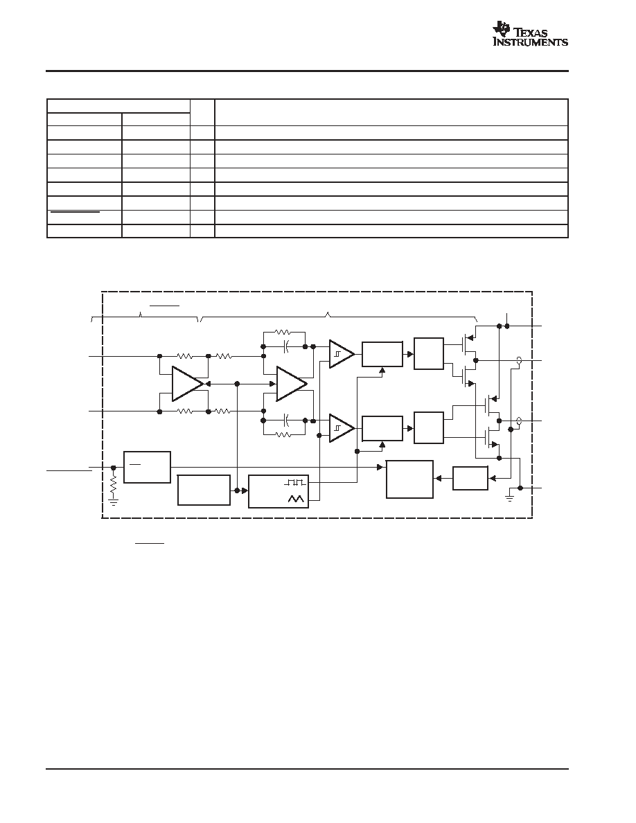
TERMINAL FUNCTIONS
TERMINAL
I/O
DESCRIPTION
NAME
YEF, YZF
I/O
DESCRIPTION
IN-
C1
I
Negative differential input
IN+
A1
I
Positive differential input
VDD
B1
I
Power supply
VO+
C3
O
Positive BTL output
GND
A2, B3
I
High-current ground
VO-
A3
O
Negative BTL output
SHUTDOWN
C2
I
Shutdown terminal (active low logic)
PVDD
B2
I
Power supply
FUNCTIONAL BLOCK DIAGRAM
_
+
_
+
_
+
_
+
150 k
150 k
_
+
_
+
Deglitch
Logic
Deglitch
Logic
Gate
Drive
Gate
Drive
V
DD
OC
Detect
Startup
Protection
Logic
Ramp
Generator
Biases
and
References
TTL
Input
Buffer
SD
*Gain = 2 V/V
B1, B2
V
DD
A3
V
O-
C3
V
O+
A2, B3
GND
C1
IN-
A1
IN+
C2
SHUTDOWN
300 k
Notes:
* Total gain =
150 k
RI
2 x
150 k
RI
*Gain =
TPA2010D1
SLOS417A - OCTOBER 2003 - REVISED DECEMBER 2003
www.ti.com
5
TYPICAL CHARACTERISTICS
TABLE OF GRAPHS
FIGURE
Efficiency
vs Output power
1, 2
PD
Power dissipation
vs Output power
3, 4
Supply current
vs Output power
5, 6
I(Q)
Quiescent current
vs Supply voltage
7
I(SD)
Shutdown current
vs Shutdown voltage
8
PO
Output power
vs Supply voltage
9
PO
Output power
vs Load resistance
10, 11
vs Output power
12, 13
THD+N
Total harmonic distortion plus noise
vs Frequency
14, 15, 16, 17
THD+N
Total harmonic distortion plus noise
vs Common-mode input voltage
18
KSVR
Supply voltage rejection ratio
vs Frequency
19, 20, 21
GSM power supply rejection
vs Time
22
GSM power supply rejection
vs Frequency
23
KSVR
Supply voltage rejection ratio
vs Common-mode input voltage
24
CMRR
Common-mode rejection ratio
vs Frequency
25
CMRR
Common-mode rejection ratio
vs Common-mode input voltage
26
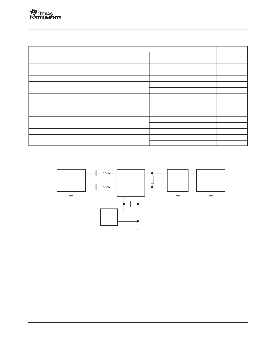
TEST SET-UP FOR GRAPHS
TPA2010D1
IN+
IN-
OUT+
OUT-
VDD
GND
CI
CI
RI
RI
Measurement
Output
+
-
1
µ
F
+
-
VDD
Load
30 kHz
Low Pass
Filter
Measurement
Input
+
-
Notes:
(1) CI was Shorted for any Common-Mode input voltage measurement
(2) A 33-
µ
H inductor was placed in series with the load resistor to emulate a small speaker for efficiency measurements.
(3) The 30-kHz low-pass filter is required even if the analyzer has an internal low-pass filter. An RC low pass filter (100
, 47 nF) is
used on each output for the data sheet graphs.