 | –≠–ª–µ–∫—Ç—Ä–æ–Ω–Ω—ã–π –∫–æ–º–ø–æ–Ω–µ–Ω—Ç: TPA2032D1 | –°–∫–∞—á–∞—Ç—å:  PDF PDF  ZIP ZIP |
www.ti.com
FEATURES
APPLICATIONS
DESCRIPTION
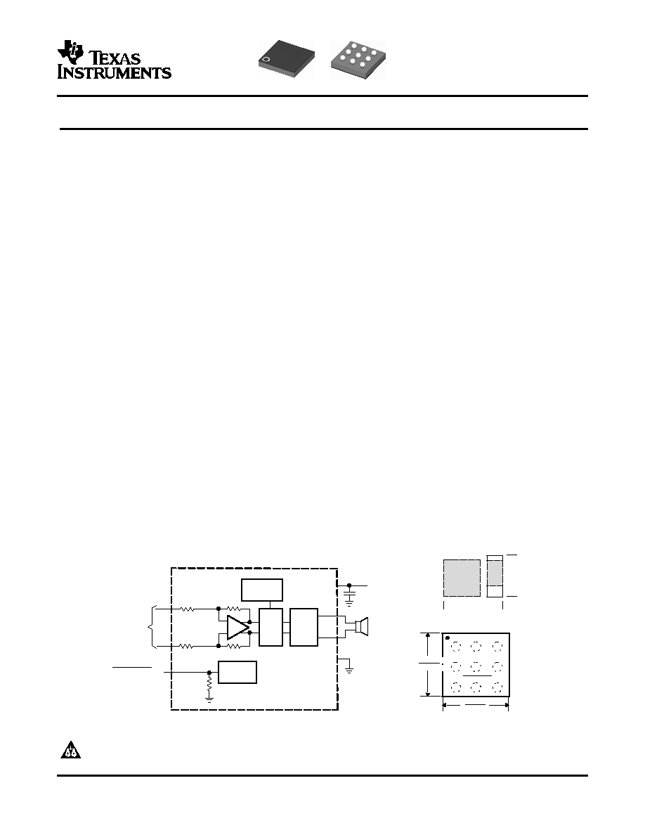
APPLICATION CIRCUIT
_
+
IN-
IN+
PWM
H-
Bridge
V
O-
V
O+
Internal
Oscillator
To Battery
V
DD
GND
Bias
Circuitry
Differential
Input
TPA2032D1
SHUTDOWN
A1
A2
A3
B1
B2
B3
C1
C2
C3
IN+
GND
V
O-
V
DD
PV
DD
PGND
IN- SHUTDWN V
O+
1,4 mm
9-BALL WAFER CHIP SCALE, YZF PACKAGE,
(TOP VIEW OF PCB)
Note: Pin A1 is marked with a "0" .
1,55 mm
1,4 mm
1,55 mm
TPA
203xD1
0402
~
2,5 mm
~
1,7mm
C
S
C
S
TPA2032D1
TPA2033D1
TPA2034D1
SLOS476 ≠ JUNE 2006
2.75-W FIXED GAIN MONO FILTER-FREE CLASS-D AUDIO POWER AMPLIFIER
∑
Wafer Chip Scale Packaging (WCSP)
∑
Maximize Battery Life and Minimize Heat
≠ NanoFreeTM Lead-Free (Pb-Free: YZF)
≠ 0.5-
µ
A Shutdown Current
≠ 3.0-mA Quiescent Current
∑
Ideal for Wireless Handsets, PDAs, and other
≠ High Efficiency Class-D
mobile devices
∑
88% at 400mW at 8
∑
80% at 100mW at 8
∑
Three Fixed Gain Versions
The TPA2032D1 (2V/V gain), TPA2033D1 (3V/V
gain), and TPA2034D1 (4V/V gain) are 2.75-W high
≠ TPA2032D1 has a gain of 2 V/V (6dB)
efficiency filter-free class-D audio power amplifiers,
≠ TPA2033D1 has a gain of 3 V/V (9.5dB)
each in an approximately 1.5-mm
◊
1.5-mm wafer
≠ TPA2034D1 has a gain of 4 V/V (12dB)
chip scale package (WCSP) that requires only one
∑
Only One External Component Required
external component. The pinout is the same as the
TPA2010D1 except that the external gain setting
≠ Internal Matched Input Gain and Feedback
input resistors required by the TPA2010D1 are
Resistors for Excellent PSRR and CMRR
integrated into the fixed gain TPA203xD1 family.
≠ Optimized PWM Output Stage Eliminates
Features
like
≠75dB
PSRR
and
improved
LC Output Filter
RF-rectification immunity with a very small PCB
≠ PSRR (≠75 dB) and Wide Supply Voltage
footprint (WCSP amplifier plus single decoupling
(2.5 V to 5.5 V) Eliminates Need for a
cap) make the TPA203xD1 family ideal for wireless
Dedicated Voltage Regulator
handsets. A fast start-up time of 3.2 ms with minimal
pop makes the TPA203xD1 family ideal for PDA
≠ Fully Differential Design Reduces RF
applications.
Rectification and Eliminates Bypass
Capacitor
In wireless handsets, the earpiece, speaker phone,
≠ CMRR (≠69 dB)Eliminates Two Input
and melody ringer can each be driven by a
TPA203xD1. The TPA203xD1 family has a low
Coupling Capacitors
27-
µ
V noise floor, A-weighted.
∑
Thermal and Short-Circuit Protection
∑
Pinout Very Similar to TPA2010D1
Please be aware that an important notice concerning availability, standard warranty, and use in critical applications of Texas
Instruments semiconductor products and disclaimers thereto appears at the end of this data sheet.
NanoFree is a trademark of Texas Instruments.
PRODUCTION DATA information is current as of publication date.
Copyright © 2006, Texas Instruments Incorporated
Products conform to specifications per the terms of the Texas
Instruments standard warranty. Production processing does not
necessarily include testing of all parameters.

www.ti.com
ORDERING INFORMATION
ABSOLUTE MAXIMUM RATINGS
RECOMMENDED OPERATING CONDITIONS
PACKAGE DISSIPATION RATINGS
TPA2032D1
TPA2033D1
TPA2034D1
SLOS476 ≠ JUNE 2006
These devices have limited built-in ESD protection. The leads should be shorted together or the device placed in conductive foam
during storage or handling to prevent electrostatic damage to the MOS gates.
T
A
PACKAGE
PART NUMBER
SYMBOL
≠40
∞
C to 85
∞
C
Wafer chip scale packaging ≠ Lead free (YZF)
TPA2032D1YZF
(1)
BPX
≠40
∞
C to 85
∞
C
Wafer chip scale packaging ≠ Lead free (YZF)
TPA2033D1YZF
(1)
BPY
≠40
∞
C to 85
∞
C
Wafer chip scale packaging ≠ Lead free (YZF)
TPA2034D1YZF
(1)
BPZ
(1)
The YZF package is only available taped and reeled. To order add the suffix R to the end of the part number for a reel of 3000, or add
the suffix T to the end of the part number for a reel of 250 (e.g. TPA2032D1YZFR).
over operating free-air temperature range unless otherwise noted
(1)
TPA2032D1, TPA2033D1,
TPA2034D1
In active mode
≠0.3 V to 6 V
V
DD
Supply voltage
In SHUTDOWN mode
≠0.3 V to 7 V
V
I
Input voltage
≠0.3 V to V
DD
+ 0.3 V
Continuous total power dissipation
See Dissipation Rating Table
T
A
Operating free-air temperature
≠40
∞
C to 85
∞
C
T
J
Operating junction temperature
≠40
∞
C to 125
∞
C
T
stg
Storage temperature
≠65
∞
C to 150
∞
C
(1)
Stresses beyond those listed under absolute maximum ratings may cause permanent damage to the device. These are stress ratings
only, and functional operation of the device at these or any other conditions beyond those indicated under recommended operating
conditions is not implied. Exposure to absolute-maximum-rated conditions for extended periods may affect device reliability.
MIN
NOM
MAX
UNIT
V
DD
Supply voltage
2.5
5.5
V
V
IH
High-level input voltage
SHUTDOWN
1.3
V
DD
V
V
IL
Low-level input voltage
SHUTDOWN
0
0.35
V
V
IC
Common mode input voltage range V
DD
= 2.5 V, 5.5 V
0.5
V
DD
≠0.8
V
T
A
Operating free-air temperature
≠40
85
∞
C
DERATING FACTOR
T
A
25
∞
C
T
A
= 70
∞
C
T
A
= 85
∞
C
PACKAGE
(1 /
JA
)
POWER RATING
POWER RATING
POWER RATING
YZF
4.8 mW/
∞
C
(1)
480 mW
264 mW
192 mW
YZF
7.5 mW/
∞
C
(2)
750 mW
412 mW
300 mW
(1)
Derating factor measured with JEDEC Low-K board; 1S0P - One signal layer and zero plane layers.
(2)
Derating factor measured with JEDEC High K board; 1S2P - One signal layer and two plane layers.
Please see JEDEC Standard 51-3 for Low-K board, JEDEC Standard 51-7 for High-K board, and JEDEC Standard 51-12 for using
package thermal information.
Please see JEDEC document page for downloadable copies: http://www.jedec.org/download/default.cfm.
2
Submit Documentation Feedback
www.ti.com
ELECTRICAL CHARACTERISTICS
OPERATING CHARACTERISTICS
TPA2032D1
TPA2033D1
TPA2034D1
SLOS476 ≠ JUNE 2006
T
A
= 25
∞
C (unless otherwise noted)
PARAMETER
TEST CONDITIONS
MIN
TYP
MAX
UNIT
TPA2032D1
5
25
Output offset voltage
|V
OS
|
Inputs AC grounded, V
DD
= 2.5 V to 5.5 V
TPA2033D1
5
25
mV
(measured differentially)
TPA2034D1
5
25
PSRR
Power supply rejection ratio
V
DD
= 2.5 V to 5.5 V
≠75
-61
dB
V
DD
= 2.5 V
≠69
-52
CMRR
Common mode rejection ratio
V
IC
= 0.5 V to (V
DD
≠0.8 V)
V
DD
= 3.6 V
≠ 69
-52
dB
V
DD
= 5.5 V
≠69
-52
|I
IH
|
High-level input current
V
DD
= 5.5 V, V
I
= 5.8 V
50
µ
A
|I
IL
|
Low-level input current
V
DD
= 5.5 V, V
I
= ≠0.3 V
5
µ
A
V
DD
= 5.5 V, no load
4
5.7
I
(Q)
Quiescent current
V
DD
= 3.6 V, no load
3
mA
V
DD
= 2.5 V, no load
2.2
3.7
I
(SD)
Shutdown current
V
(SHUTDOWN)
= 0.35 V, V
DD
= 2.5 V to 5.5 V
0.5
0.8
µ
A
V
DD
= 2.5 V
550
Static drain-source on-state
r
DS(on)
V
DD
= 3.6 V
420
m
resistance
V
DD
= 5.0 V
350
Output impedance in
V
(SHUTDOWN)
<= 0.35 V
2
k
SHUTDOWN
f
(sw)
Switching frequency
V
DD
= 2.5 V to 5.5 V
240
300
400
kHz
TPA2032D1
5.5
6
6.5
Gain
V
DD
= 2.5 V to 5.5 V
TPA2033D1
9.0
9.5
10.0
dB
TPA2034D1
11.5
12
12.5
Resistance of internal pulldown
R
PD
resistor from shutdown pin to
300
k
GND
T
A
= 25
∞
C, R
L
= 8
(unless otherwise noted)
PARAMETER
TEST CONDITIONS
MIN
TYP
MAX
UNIT
V
DD
= 5 V
2.75
R
L
= 4
, THD + N = 10%, f = 1 kHz
V
DD
= 3.6 V
1.35
W
V
DD
= 2.5 V
0.59
V
DD
= 5 V
2.25
R
L
= 4
, THD + N = 1%, f = 1 kHz
V
DD
= 3.6 V
1.12
W
V
DD
= 2.5 V
0.48
P
O
Output power
V
DD
= 5 V
1.68
R
L
= 8
, THD + N = 10%, f = 1 kHz
V
DD
= 3.6 V
0.85
W
V
DD
= 2.5 V
0.38
V
DD
= 5 V
1.37
R
L
= 8
, THD + N = 1%, f = 1 kHz
V
DD
= 3.6 V
0.68
W
V
DD
= 2.5 V
0.31
V
DD
= 5 V, P
O
= 1 W, R
L
= 8
, f = 1 kHz
0.18%
THD+
Total harmonic distortion plus
V
DD
= 3.6 V, P
O
= 0.5 W, R
L
= 8
, f = 1 kHz
0.11%
N
noise
V
DD
= 2.5 V, P
O
= 200 mW, R
L
= 8
, f = 1 kHz
0.10%
V
DD
= 3.6 V, Inputs AC grounded
f = 217 Hz,
k
SVR
Supply ripple rejection ratio
≠73
dB
with C
I
= 1
µ
F
V
(RIPPLE)
= 200 mV
pp
SNR
Signal-to-noise ratio
V
DD
= 5 V, P
O
= 1 W, R
L
= 8
, A weighted noise
100
dB
3
Submit Documentation Feedback

www.ti.com
FUNCTIONAL BLOCK DIAGRAM
Input
Buffer
SC
300 K
TPA2032D1
TPA2033D1
TPA2034D1
SLOS476 ≠ JUNE 2006
OPERATING CHARACTERISTICS (continued)
T
A
= 25
∞
C, R
L
= 8
(unless otherwise noted)
PARAMETER
TEST CONDITIONS
MIN
TYP
MAX
UNIT
No weighting
35
V
DD
= 3.6 V, f = 20 Hz to 20 kHz,
V
n
Output voltage noise
µ
V
RMS
Inputs AC grounded with C
i
= 1
µ
F
A weighting
27
V
DD
= 3.6 V, V
IC
= 1.0 V
pp
, V
Cm
= 1.8
CMRR Common mode rejection ratio
f = 217 Hz
≠69
dB
V
A
V
= 2 V/V
30.2
R
I
Input impedance
A
V
= 3 V/V
22.8
k
A
V
= 4 V/V
18.5
Start-up time from shutdown
V
DD
= 3.6 V
3.2
ms
Terminal Functions
TERMINAL
I/O
DESCRIPTION
NAME
YZF
IN≠
C1
I
Negative differential audio input
IN+
A1
I
Positive differential audio input
V
O-
A3
O
Negative BTL audio output
V
O+
C3
O
Positive BTL audio output
Analog ground terminal. Must be connected to same potential as PGND using a direct connection
GND
A2
I
to a single point ground.
High-current Analog ground terminal. Must be connected to same potential as GND using a direct
PGND
B3
connection to a single point ground.
V
DD
B1
I
Power supply terminal. Must be connected to same power supply as PV
DD
using a direct
connection. Voltage must be within values listed in Recommended Operating Conditions table.
High-current Power supply terminal. Must be connected to same power supply as V
DD
using a
PV
DD
B2
I
direct connection. Voltage must be within values listed in Recommended Operating Conditions
table.
SHUTDOWN
C2
I
Shutdown terminal. When terminal is low the device is put into Shutdown mode.
4
Submit Documentation Feedback

www.ti.com
TYPICAL CHARACTERISTICS
TABLE OF GRAPHS
TEST SET-UP FOR GRAPHS
TPA2032D1
IN+
IN -
OUT+
OUT -
V
DD
GND
C
I
C
I
Measurement
Output
+
-
1 mF
+
-
V
DD
Load
30 kHz
Low Pass
Filter
Measurement
Input
+
-
TPA2032D1
TPA2033D1
TPA2034D1
SLOS476 ≠ JUNE 2006
FIGURE
Efficiency
vs Output power
1, 2
P
D
Power dissipation
vs Output power
3, 4
Supply current
vs Output power
5, 6
I
DD
Supply current
vs Supply voltage
7
I
(SD)
Shutdown current
vs Shutdown voltage
8
vs Load resistance
9, 10
P
O
Output power
vs Supply voltage
11
vs Output power
12, 13
THD+N
Total harmonic distortion plus noise
vs Frequency
14, 15, 16, 17
vs Common-mode input voltage
18
19, 20, 21, 22, 23, 24, 25,
K
SVR
Supply voltage rejection ratio
vs Frequency
26, 27
vs Time
28
GSM power supply rejection
vs Frequency
29
K
SVR
Supply voltage rejection ratio
vs Common-mode input voltage
30, 31, 32
vs Frequency
33
CMRR
Common-mode rejection ratio
vs Common-mode input voltage
34
(1)
C
I
was shorted for any common-mode input voltage measurement. All other measurements were taken with a 1-
µ
F
C
I
(unless otherwise noted).
(2)
A 33-
µ
H inductor was placed in series with the load resistor to emulate a small speaker for efficiency measurements.
(3)
The 30-kHz low-pass filter is required, even if the analyzer has an internal low-pass filter. An RC low-pass filter
(100
, 47-nF) is used on each output for the data sheet graphs.
5
Submit Documentation Feedback