 | –≠–ª–µ–∫—Ç—Ä–æ–Ω–Ω—ã–π –∫–æ–º–ø–æ–Ω–µ–Ω—Ç: TPA4411 | –°–∫–∞—á–∞—Ç—å:  PDF PDF  ZIP ZIP |
www.ti.com
FEATURES
APPLICATIONS
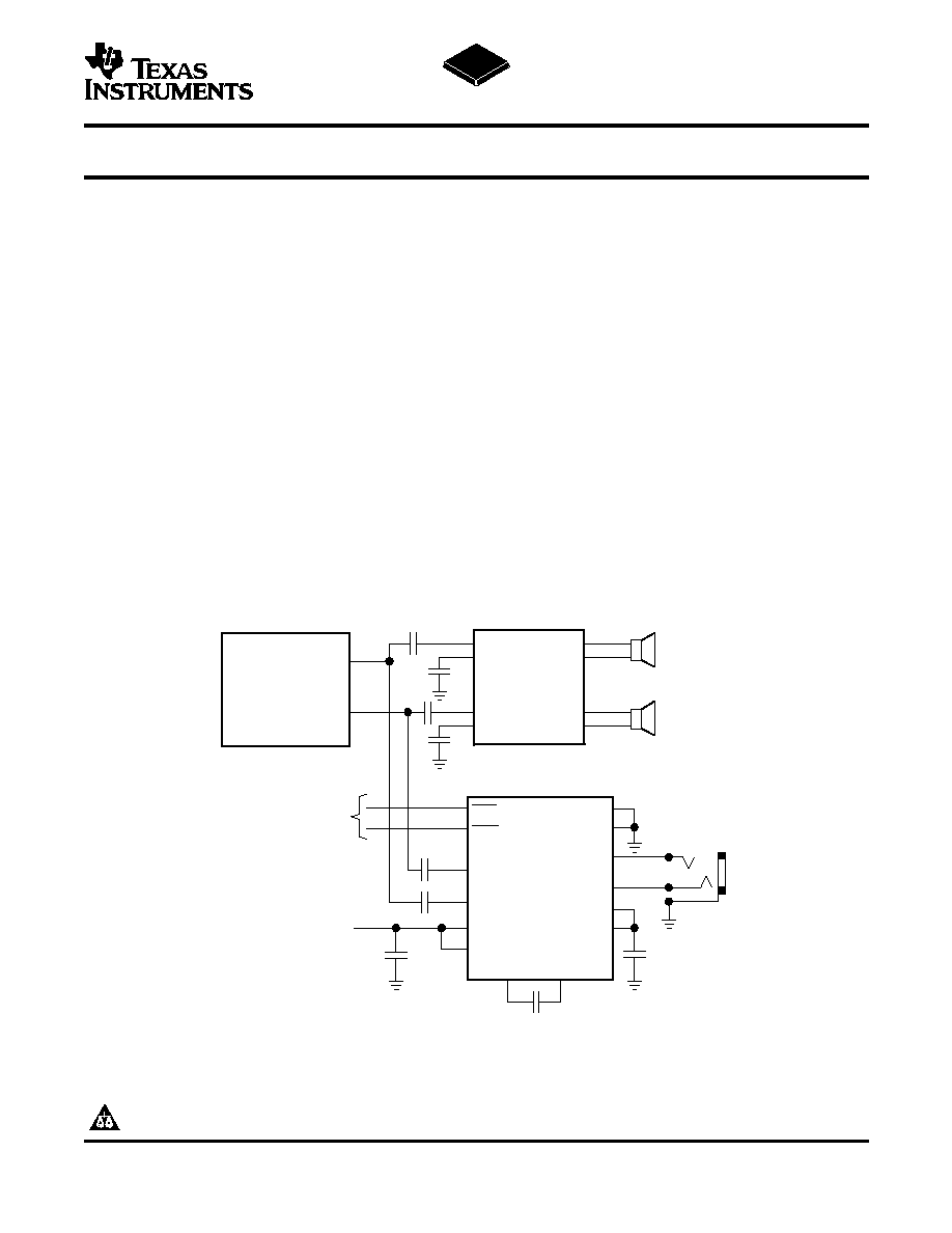
DESCRIPTION
Shutdown
Control
SV
DD
PV
DD
C1P
C1N
SV
SS
PV
SS
OUTR
OUTL
SDR
INL
INR
SDL
1.8 - 4.5 V
TPA4411
TPA2012D2
TLV320AIC26
or
TLV320AIC28
HPL
or
SPK1
HPR
or
SPK2
PGND
SGND
TPA4411
SLOS430 ≠ AUGUST 2004
80-mW CAPLESS STEREO HEADPHONE DRIVER
∑
Ground-Referenced Outputs Eliminate
∑
Notebook Computers
DC-Bias Voltages on Headphone Ground Pin
∑
CD / MP3 Players
≠ No Output DC-Blocking Capacitors
∑
Smart Phones
∑
Reduced Board Area
∑
Cellular Phones
∑
Reduced Component Cost
∑
PDAs
∑
Improved THD+N Performance
∑
No Degradation of Low-Frequency
Response Due to Output Capacitors
The TPA4411 is a stereo headphone driver designed
∑
Wide Power Supply Range: 1.8 V to 4.5 V
to allow the removal of the output dc-blocking capaci-
∑
80-mW/Ch Output Power into 16-
at 4.5 V
tors for reduced component count and cost. The
TPA4411 is ideal for small portable electronics where
∑
Independent Right and Left Channel
size and cost are critical design parameters.
Shutdown Control
∑
Short-Circuit and Thermal Protection
The TPA4411 is capable of driving 80 mW into a
16-
load at 4.5 V. The TPA4411 has a fixed gain of
∑
Pop Reduction Circuitry
-1.5 V/V and headphone outputs have
±
8-kV IEC
∑
Space Saving Pb-Free Packages
ESD protection. The TPA4411 has independent shut-
≠ 20-pin, 4 mm
◊
4 mm ThinQFN
down control for the right and left audio channels.
≠ 16-ball, 2 mm
◊
2 mm WCSP
The TPA4411 is available in a 20-pin, 4 mm
◊
4 mm
(Product Preview)
ThinQFN package.
.
Please be aware that an important notice concerning availability, standard warranty, and use in critical applications of Texas
Instruments semiconductor products and disclaimers thereto appears at the end of this data sheet.
UNLESS OTHERWISE NOTED this document contains PRO-
Copyright © 2004, Texas Instruments Incorporated
DUCTION DATA information current as of publication date. Prod-
ucts conform to specifications per the terms of Texas Instruments
standard warranty. Production processing does not necessarily
include testing of all parameters.

www.ti.com
INR
INL
PGND
OUTL
PVSS
SVSS
C1N
PVDD
SGND
A1
B1
C1
D1
A2
A3
A4
SDL
SVDD
C1P
SDR
NC - No internal connection
NC
NC
OUTR
20
19
18
17
16
15
14
13
12
11
10
9
8
7
6
5
4
3
2
1
NC
PVDD
SDL
SGND
NC
C1P
PGND
C1N
NC
PVSS
INR
SDR
INL
NC
OUTR
NC
SVSS
NC
OUTL
SVDD
NC - No internal connection
TPA4411
SLOS430 ≠ AUGUST 2004
These devices have limited built-in ESD protection. The leads should be shorted together or the device
placed in conductive foam during storage or handling to prevent electrostatic damage to the MOS gates.
RTJ (QFN) PACKAGE
YZH (WCSP) PACKAGE
(TOP VIEW)
(TOP VIEW)
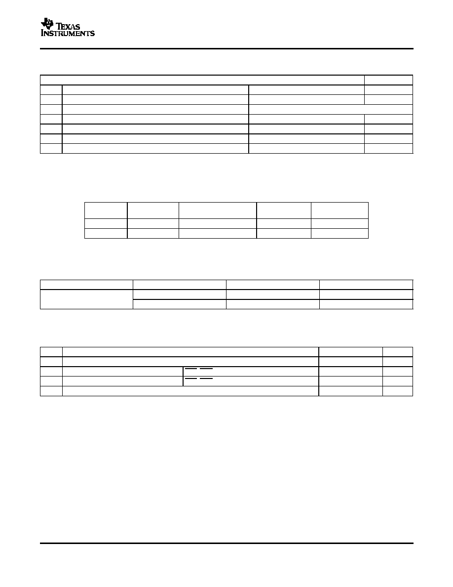
TERMINAL FUNCTIONS
TERMINAL
I/O
DESCRIPTION
NAME
QFN
WCSP
(1)
C1P
1
A4
I/O
Charge pump flying capacitor positive terminal
PGND
2
B4
I
Power ground, connect to ground.
C1N
3
C4
I/O
Charge pump flying capacitor negative terminal
4, 6, 8, 12,
NC
B3, C3
No connection
16, 20
PVSS
5
D4
O
Output from charge pump.
SVSS
7
D3
I
Amplifier negative supply, connect to PVSS via star connection.
OUTL
9
D2
O
Left audio channel output signal
SVDD
10
D1
I
Amplifier positive supply, connect to PVDD via star connection.
OUTR
11
C2
O
Right audio channel output signal
INL
13
C1
I
Left audio channel input signal
SDR
14
B1
I
Right channel shutdown, active low logic.
INR
15
A1
I
Right audio channel input signal
SGND
17
A2
I
Signal ground, connect to ground.
SDL
18
B2
I
Left channel shutdown, active low logic.
PVDD
19
A3
I
Supply voltage, connect to positive supply.
Exposed pad must be soldered to a floating plane. Do NOT connect to power or
Exposed Pad
-
ground.
(1)
Package not yet available
2
www.ti.com
ABSOLUTE MAXIMUM RATINGS
(1)
DISSIPATION RATINGS TABLE
RECOMMENDED OPERATING CONDITIONS
TPA4411
SLOS430 ≠ AUGUST 2004
over operating free-air temperature range, T
A
= 25
∞
C (unless otherwise noted)
UNIT
Supply voltage, AVDD, PVDD
-0.3 to 5.5
V
V
I
Input voltage
-0.3 to V
DD
+ 0.3
V
Output Continuous total power dissipation
See Dissipation Rating Table
T
A
Operating free-air temperature range
- 40 to 85
∞
C
T
J
Operating junction temperature range
- 40 to 150
∞
C
T
stg
Storage temperature range
-65 to 85
∞
C
Lead temperature 1,6 mm (1/16 inch) from case for 10 seconds
260
∞
C
(1)
Stresses beyond those listed under "absolute maximum ratings" may cause permanent damage to the device. These are stress ratings
only, and functional operation of the device at these or any other conditions beyond those indicated under "recommended operating
conditions" is not implied. Exposure to absolute-maximum-rated conditions for extended periods may affect device reliability.
T
A
25
∞
C
DERATING FACTOR
(1)
T
A
= 70
∞
C
T
A
= 85
∞
C
PACKAGE
POWER RATING
POWER RATING
POWER RATING
RTJ
3450 mW
34.5 mW/
∞
C
1898 mW
1380 mW
YZH
(2)
TBD
TBD mW/
∞
C
TBD
TBD
(1)
Derating factor measured with High K board.
(2)
Product preview
AVAILABLE OPTIONS
T
A
PACKAGED DEVICES
PART NUMBER
SYMBOL
20-pin, 4 mm
◊
4 mm QFN
TPA4411RTJ
(1)
AKQ
-40
∞
C to 85
∞
C
16-ball, 2 mm
◊
2mm WSCP
TPA4411YZH
AKT
(1)
The RTJ package is only available taped and reeled. To order, add the suffix "R" to the end of the part number for a reel of 3000, or add
the suffix "T" to the end of the part number for a reel of 250 (e.g., TPA4411RTJR).
MIN
MAX
UNIT
Supply voltage, AVDD, PVDD
1.8
4.5
(1)
V
V
IH
High-level input voltage
SDL, SDR
1.5
V
V
IL
Low-level input voltage
SDL, SDR
0.5
V
T
A
Operating free-air temperature
- 40
85
∞
C
(1)
Device can shut down for VDD > 4.5 V to prevent damage to the device.
3

www.ti.com
ELECTRICAL CHARACTERISTICS
OPERATING CHARACTERISTICS
TPA4411
SLOS430 ≠ AUGUST 2004
T
A
= 25
∞
C (unless otherwise noted)
PARAMETER
TEST CONDITIONS
MIN
TYP
MAX
UNIT
|VOS|
Output offset voltage
V
DD
= 1.8 V to 4.5 V, Inputs grounded
8
mV
PSRR
Power Supply Rejection Ratio
V
DD
= 1.8 V to 4.5 V
-69
-80
dB
V
OH
High-level output voltage
V
DD
= 3 V, R
L
= 16
2.2
V
V
OL
Low-level output voltage
V
DD
= 3 V, R
L
= 16
-1.1
V
High-level input current
|I
IH
|
V
DD
= 4.5 V, V
I
= V
DD
1
µA
(SDL, SDR)
Low-level input current
|I
IL
|
V
DD
= 4.5 V, V
I
= 0 V
1
µA
(SDL, SDR)
V
DD
= 1.8 V, No load, SDL= SDR = V
DD
5.3
6.5
V
DD
= 3 V, No load, SDL = SDR = V
DD
6.5
8.0
mA
I
DD
Supply Current
V
DD
= 4.5 V, No load, SDL = SDR = V
DD
8.0
10.0
Shutdown mode, V
DD
= 1.8 V to 4.5 V
1
µA
V
DD
= 3 V , T
A
= 25
∞
C, R
L
= 16
(unless otherwise noted)
PARAMETER
TEST CONDITIONS
MIN
TYP
MAX
UNIT
THD = 1%, V
DD
= 3 V, f = 1 kHz
50
THD = 1%, V
DD
= 4.5 V, f = 1 kHz
80
P
O
Output power (Outputs In Phase)
mW
THD = 1%, V
DD
= 3 V, f = 1 kHz,
40
R
L
= 32
P
O
= 25 mW, f = 1 kHz
0.054%
Total harmonic distortion plus
THD+N
noise
P
O
= 25 mW, f = 20 kHz
0.010%
Crosstallk
P
O
= 20 mW, f = 1 kHz
-83
dB
200-mV
pp
ripple, f = 217 Hz
-82.5
k
SVR
Supply ripple rejection ratio
200-mV
pp
ripple, f = 1 kHz
-70.4
dB
200-mV
pp
ripple, f = 20 kHz
-45.1
A
v
Closed-loop voltage gain
-1.45
-1.5
-1.55
V/V
A
v
Gain matching
1%
Slew rate
2.2
V/µs
Maximum capacitive load
400
pF
V
n
Noise output voltage
10
µV
RMS
Electrostatic discharge, IEC
OUTR, OUTL
±
8
kV
f
osc
Charge pump switching frequency
280
320
420
kHz
Start-up time from shutdown
450
µs
Input impedance
12
15
18
k
SNR
Signal-to-noise ratio
P
o
= 40 mW (THD+N = 0.1%)
98
dB
Threshold
150
170
∞
C
Thermal shutdown
Hysteresis
15
∞
C
4

www.ti.com
_
+
_
+
SVDD
SVSS
SVDD
SVSS
Charge
Pump
Bias
Circuitry
TPA4411
SGND
Av = -1.5 V/V
Audio Out - R
Audio Out - L
C1P
C1N
PVSS
Audio In - R
Audio In - L
SDx
Short
Circuit
Protection
TYPICAL CHARACTERISTICS
Table of Graphs
TPA4411
SLOS430 ≠ AUGUST 2004
Functional Block Diagram
C
(PUMP)
= C
(PVSS)
= 2.2 µF , C
IN
= 1 µF (unless otherwise noted)
FIGURE
Total harmonic distortion + noise
vs Output power
1 - 24
Total harmonic distortion + noise
vs Frequency
25 - 32
Supply voltage rejection ratio
vs Frequency
33, 34
Power dissipation
vs Output power
35 - 42
Crosstalk
vs Frequency
43 - 46
Output power
vs Supply voltage
47 - 50
Quiescent supply current
vs Supply voltage
51
Output power
vs Load resistance
52 - 60
Output spectrum
61
Gain and phase
vs Frequency
62, 63
5