 | –≠–ª–µ–∫—Ç—Ä–æ–Ω–Ω—ã–π –∫–æ–º–ø–æ–Ω–µ–Ω—Ç: TPA6100A2 | –°–∫–∞—á–∞—Ç—å:  PDF PDF  ZIP ZIP |
Please be aware that an important notice concerning availability, standard warranty, and use in critical applications of
Texas Instruments semiconductor products and disclaimers thereto appears at the end of this data sheet.
TPA6100A2
50-mW ULTRALOW VOLTAGE STEREO HEADPHONE
AUDIO POWER AMPLIFIER
SLOS269A ≠ JUNE 2000 ≠ REVISED NOVEMBER 2000
1
POST OFFICE BOX 655303
∑
DALLAS, TEXAS 75265
D
50-mW Stereo Output
D
Low Supply Current . . . 0.75 mA
D
Low Shutdown Current . . . 50
nA
D
Pin Compatible With LM4881 and TPA102
D
Pop Reduction Circuitry
D
Internal Mid-Rail Generation
D
Thermal and Short-Circuit Protection
D
Surface-Mount Packaging
≠ MSOP
≠ SOIC
D
1.6-V to 3.6-V Supply Voltage Range
The polarity of the SHUTDOWN pin is reversed.
description
The TPA6100A2 is a stereo audio power amplifier packaged in either an 8-pin SOIC package or an 8-pin MSOP
package capable of delivering 50 mW of continuous RMS power per channel into 16-
loads. Amplifier gain
is externally configured by a means of three resistors per input channel and does not require external
compensation for settings of 1 to 10.
The TPA6100A2 is optimized for battery applications because of its low supply current, shutdown current, and
THD+N. To obtain the low-supply voltage range, the TPA6100A2 biases BYPASS to V
DD
/4. A resistor with a
resistance equal to R
F
must be added from the inputs to ground to allow the output to be biased at V
DD
/2.
When driving a 16-
load with 45-mW output power from 3.3 V, THD+N is 0.04% at 1 kHz, and less than 0.2%
across the audio band of 20 Hz to 20 kHz. For 28 mW into 32-
loads, the THD+N is reduced to less than 0.03%
at 1 kHz, and is less than 0.2% across the audio band of 20 Hz to 20 kHz.
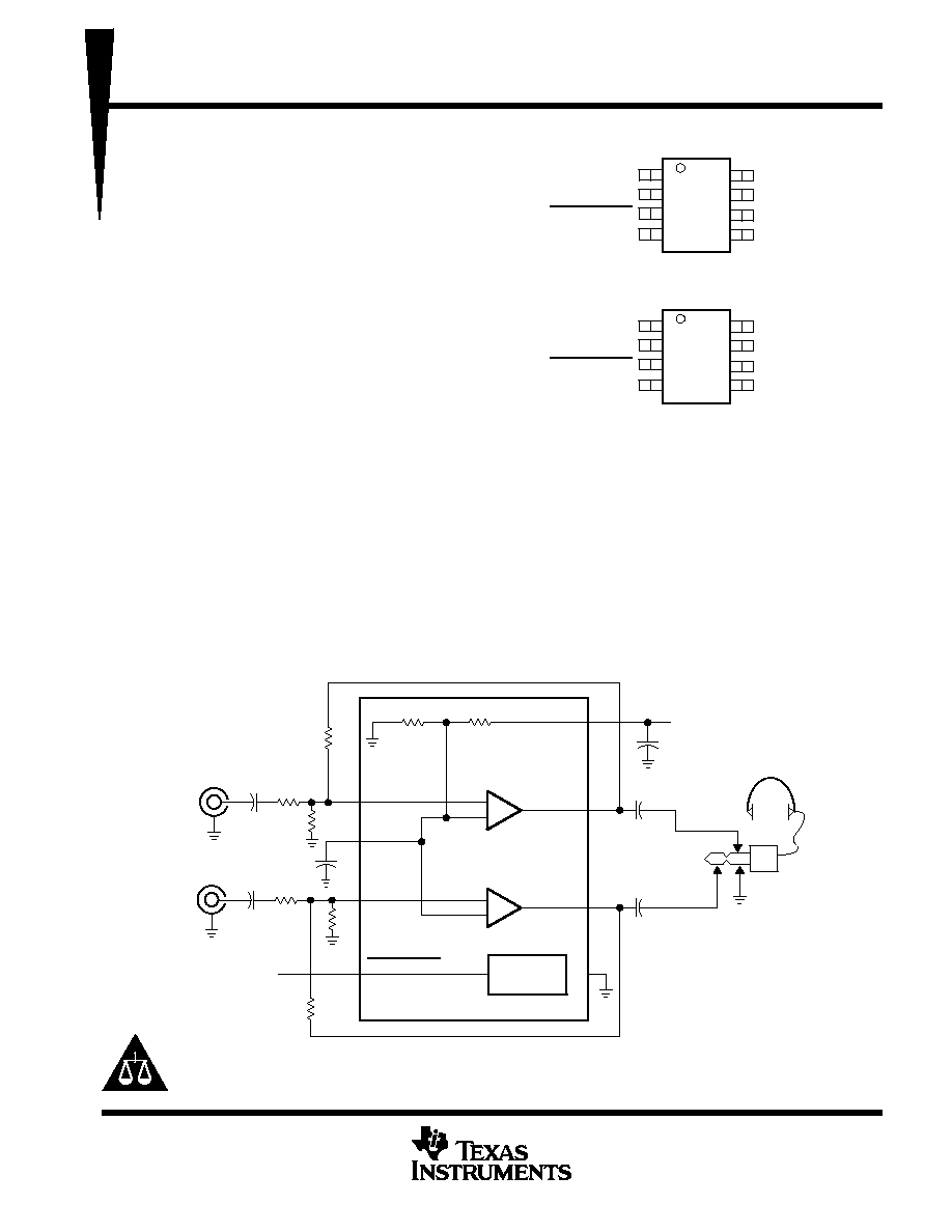
typical application circuit
Audio
Input
Bias
Control
6
7
5
2
VO1
VO2
VDD
3
8
1
4
IN 1≠
BYPASS
SHUTDOWN
VDD/4
CI
RI
RF
CB
CS
Audio
Input
CI
RI
IN 2≠
RF
VDD
From Shutdown
Control Circuit
≠
+
≠
+
CC
CC
R
R
Copyright
2000, Texas Instruments Incorporated
1
2
3
4
8
7
6
5
BYPASS
GND
SHUTDOWN
IN2≠
IN1≠
V
O
1
V
DD
V
O
2
DGK PACKAGE
(TOP VIEW)
1
2
3
4
8
7
6
5
BYPASS
GND
SHUTDOWN
IN2≠
IN1≠
V
O
1
V
DD
V
O
2
D PACKAGE
(TOP VIEW)
PRODUCTION DATA information is current as of publication date.
Products conform to specifications per the terms of Texas Instruments
standard warranty. Production processing does not necessarily include
testing of all parameters.
TPA6100A2
50-mW ULTRALOW VOLTAGE STEREO HEADPHONE
AUDIO POWER AMPLIFIER
SLOS269A ≠ JUNE 2000 ≠ REVISED NOVEMBER 2000
2
POST OFFICE BOX 655303
∑
DALLAS, TEXAS 75265
AVAILABLE OPTIONS
TA
PACKAGED DEVICE
MSOP
TA
SMALL OUTLINE (D)
MSOP (DGK)
SYMBOLIZATION
≠ 40
∞
C to 85
∞
C
TPA6100A2D
TPA6100A2DGK
AJL
Terminal Functions
TERMINAL
I/O
DESCRIPTION
NAME
NO.
I/O
DESCRIPTION
BYPASS
1
I
Tap to voltage divider for internal mid-supply bias supply. BYPASS is set at VDD/4. Connect to a
0.1-
µ
F to 1-
µ
F low-ESR capacitor for best performance.
GND
2
I
GND is the ground connection.
IN1≠
8
I
IN1≠ is the inverting input for channel 1.
IN2≠
4
I
IN2≠ is the inverting input for channel 2.
SHUTDOWN
3
I
Active-low input. When held low, the device is placed in a low supply current mode.
VDD
6
I
VDD is the supply voltage terminal.
VO1
7
O
VO1 is the audio output for channel 1.
VO2
5
O
VO2 is the audio output for channel 2.
absolute maximum ratings over operating free-air temperature (unless otherwise noted)
Supply voltage, V
DD
4 V
. . . . . . . . . . . . . . . . . . . . . . . . . . . . . . . . . . . . . . . . . . . . . . . . . . . . . . . . . . . . . . . . . . . . . . . .
Input voltage, V
I
≠ 0.3 V to V
DD
+ 0.3 V
. . . . . . . . . . . . . . . . . . . . . . . . . . . . . . . . . . . . . . . . . . . . . . . . . . . . . . . . . . .
Continuous total power dissipation
Internally Limited
. . . . . . . . . . . . . . . . . . . . . . . . . . . . . . . . . . . . . . . . . . . . . . . .
Operating junction temperature range, T
J
≠ 40
∞
C to 150
∞
C
. . . . . . . . . . . . . . . . . . . . . . . . . . . . . . . . . . . . . . . . . . .
Storage temperature range, T
stg
≠ 65
∞
C to 150
∞
C
. . . . . . . . . . . . . . . . . . . . . . . . . . . . . . . . . . . . . . . . . . . . . . . . . . .
Lead temperature 1,6 mm (1/16 inch) from case for 10 seconds
260
∞
C
. . . . . . . . . . . . . . . . . . . . . . . . . . . . . . .
Stresses beyond those listed under "absolute maximum ratings" may cause permanent damage to the device. These are stress ratings only, and
functional operation of the device at these or any other conditions beyond those indicated under "recommended operating conditions" is not
implied. Exposure to absolute-maximum-rated conditions for extended periods may affect device reliability.
DISSIPATION RATING TABLE
PACKAGE
TA
25
∞
C
POWER RATING
DERATING FACTOR
ABOVE TA = 25
∞
C
TA = 70
∞
C
POWER RATING
TA = 85
∞
C
POWER RATING
D
710 mW
5.68 mW/
∞
C
454 mW
369 mW
DGK
469 mW
3.75 mW/
∞
C
300 mW
244 mW
recommended operating conditions
MIN
MAX
UNIT
¡¡¡¡¡¡¡¡¡¡¡¡¡¡¡¡¡¡¡¡¡¡¡¡¡¡¡¡
¡¡¡¡¡¡¡¡¡¡¡¡¡¡¡¡¡¡¡¡¡¡¡¡¡¡¡¡
Supply voltage, VDD
¡¡¡
¡¡¡
1.6
¡¡¡
¡¡¡
3.6
¡¡¡
¡¡¡
V
¡¡¡¡¡¡¡¡¡¡¡¡¡¡¡¡¡¡¡¡¡¡¡¡¡¡¡¡
¡¡¡¡¡¡¡¡¡¡¡¡¡¡¡¡¡¡¡¡¡¡¡¡¡¡¡¡
Operating free-air temperature, TA
¡¡¡
¡¡¡
≠ 40
¡¡¡
¡¡¡
85
¡¡¡
¡¡¡
∞
C
TPA6100A2
50-mW ULTRALOW VOLTAGE STEREO HEADPHONE
AUDIO POWER AMPLIFIER
SLOS269A ≠ JUNE 2000 ≠ REVISED NOVEMBER 2000
3
POST OFFICE BOX 655303
∑
DALLAS, TEXAS 75265
dc electrical characteristics at T
A
= 25
∞
C, V
DD
= 3.3 V
PARAMETER
TEST CONDITIONS
MIN
TYP
MAX
UNIT
PSRR
Power supply rejection ratio
VDD = 3.0 V to 3.6 V
72
dB
IDD
Supply current
0.75
1.2
mA
IDD(SD)
Supply current in SHUTDOWN mode
50
250
nA
|IIH|
High-level input current (SHUTDOWN)
VDD = 3.3 V, VI= VDD
1
µ
A
|IIL|
Low-level input current (SHUTDOWN)
VDD = 3.3 V, VI= 0 V
1
µ
A
ZI
Input impedance (IN1≠, IN2≠)
> 1
M
ac operating characteristics, V
DD
= 3.3 V, T
A
= 25
∞
C, R
L
= 16
PARAMETER
TEST CONDITIONS
MIN
TYP
MAX
UNIT
PO
Output power (each channel)
THD
0.1%,
f = 1 kHz
50
mW
THD+N
Total harmonic distortion + noise
PO = 45 mW,
20≠20 kHz
0.2%
BOM
Maximum output power BW
G = 1,
THD < 0.5%
> 20
kHz
kSVR
Supply ripple rejection
f = 1 kHz
52
dB
SNR
Signal-to-noise ratio
PO = 50 mW
90
dB
Vn
Noise output voltage (no noise weighting filter)
28
µ
V(rms)
ac operating characteristics, V
DD
= 3.3 V, T
A
= 25
∞
C, R
L
= 32
PARAMETER
TEST CONDITIONS
MIN
TYP
MAX
UNIT
PO
Output power (each channel)
THD
0.1%,
f = 1 kHz
35
mW
THD+N
Total harmonic distortion + noise
PO = 30 mW,
20≠20 kHz
0.2%
BOM
Maximum output power BW
G = 1,
THD < 0.2%
> 20
kHz
kSVR
Supply ripple rejection
f = 1 kHz
52
dB
SNR
Signal-to-noise ratio
PO = 35 mW
91
dB
Vn
Noise output voltage (no noise weighting filter)
28
µ
V(rms)
TPA6100A2
50-mW ULTRALOW VOLTAGE STEREO HEADPHONE
AUDIO POWER AMPLIFIER
SLOS269A ≠ JUNE 2000 ≠ REVISED NOVEMBER 2000
4
POST OFFICE BOX 655303
∑
DALLAS, TEXAS 75265
dc electrical characteristics at T
A
= 25
∞
C, V
DD
= 1.6 V
PARAMETER
TEST CONDITIONS
MIN
TYP
MAX
UNIT
PSRR
Power supply rejection ratio
VDD = 1.5 V to 1.7 V
80
dB
IDD
Supply current
1.2
mA
IDD(SD)
Supply current in SHUTDOWN mode
50
250
nA
|IIH|
High-level input current (SHUTDOWN)
VDD = 1.6 V, VI= VDD
1
µ
A
|IIL|
Low-level input current (SHUTDOWN)
VDD = 1.6 V, VI= 0 V
1
µ
A
ZI
Input impedance (IN1≠, IN2≠)
> 1
M
ac operating characteristics, V
DD
= 1.6 V, T
A
= 25
∞
C, R
L
= 16
PARAMETER
TEST CONDITIONS
MIN
TYP
MAX
UNIT
PO
Output power (each channel)
THD
0.1%,
f = 1 kHz
9.5
mW
THD+N
Total harmonic distortion + noise
PO = 9.5 mW,
20≠20 kHz
0.4%
BOM
Maximum output power BW
G = 0 dB,
THD < 0.4%
> 20
kHz
kSVR
Supply ripple rejection
f = 1 kHz
53
dB
SNR
Signal-to-noise ratio
PO = 9.5 mW
86
dB
Vn
Noise output voltage (no noise weighting filter)
18
µ
V(rms)
ac operating characteristics, V
DD
= 1.6 V, T
A
= 25
∞
C, R
L
= 32
PARAMETER
TEST CONDITIONS
MIN
TYP
MAX
UNIT
PO
Output power (each channel)
THD
0.1%,
f = 1 kHz
7.1
mW
THD+N
Total harmonic distortion + noise
PO = 6.5 mW,
20≠20 kHz
0.3%
BOM
Maximum output power BW
G = 0 dB,
THD < 0.3%
> 20
kHz
kSVR
Supply ripple rejection
f = 1 kHz
53
dB
SNR
Signal-to-noise ratio
PO = 7.1 mW
88
dB
Vn
Noise output voltage (no noise weighting filter)
18
µ
V(rms)
TPA6100A2
50-mW ULTRALOW VOLTAGE STEREO HEADPHONE
AUDIO POWER AMPLIFIER
SLOS269A ≠ JUNE 2000 ≠ REVISED NOVEMBER 2000
5
POST OFFICE BOX 655303
∑
DALLAS, TEXAS 75265
APPLICATION INFORMATION
gain setting resistors, R
F
, R
I,
and R
The voltage gain for the TPA6100A2 is set by resistors R
F
and R
I
according to equation 1.
(1)
Gain
+ *
R
F
R
I
or Gain (dB)
+
20 log
R
F
R
I
Given that the TPA6100A2 is a MOS amplifier, the input impedance is very high. Consequently input leakage
currents are not generally a concern, although noise in the circuit increases as the value of R
F
increases. In
addition, a certain range of R
F
values is required for proper start-up operation of the amplifier. Taken together
it is recommended that the effective impedance seen by the inverting node of the amplifier be set between
5 k
and 20 k
. The effective impedance is calculated in equation 2.
(2)
Effective Impedance
+
R
F
R
I
R
F
)
R
I
As an example, consider an input resistance of 20 k
and a feedback resistor of 20 k
. The gain of the amplifier
would be ≠ 1 and the effective impedance at the inverting terminal would be 10 k
, which is within the
recommended range.
For high performance applications, metal film resistors are recommended because they tend to have lower
noise levels than carbon resistors. For values of R
F
above 50 k
, the amplifier tends to become unstable due
to a pole formed from R
F
and the inherent input capacitance of the MOS input structure. For this reason, a small
compensation capacitor of approximately 5 pF should be placed in parallel with R
F
. This, in effect, creates a
low-pass filter network with the cutoff frequency defined in equation 3.
(3)
f
c
+
1
2
p
R
F
C
F
For example, if R
F
is 100 k
and C
F
is 5 pF then f
c
is 318 kHz, which is well outside the audio range.
For maximum signal swing and output power at low supply voltages like 1.6 V to 3.3 V, BYPASS is biased to
V
DD
/4. However, to allow the output to be biased at V
DD
/2, a resistor, R, equal to R
F
must be placed from the
negative input to ground.
input capacitor, C
I
In the typical application, an input capacitor, C
I
, is required to allow the amplifier to bias the input signal to the
proper dc level for optimum operation. In this case, C
I
and R
I
form a high-pass filter with the corner frequency
determined in equation 4.
(4)
f
c
+
1
2
p
R
I
C
I
The value of C
I
is important to consider, as it directly affects the bass (low frequency) performance of the circuit.
Consider the example where R
I
is 20 k
and the specification calls for a flat bass response down to 20 Hz.
Equation 4 is reconfigured as equation 5.
(5)
C
I
+
1
2
p
R
I
f
c