 | –≠–ª–µ–∫—Ç—Ä–æ–Ω–Ω—ã–π –∫–æ–º–ø–æ–Ω–µ–Ω—Ç: TPA6112A2 | –°–∫–∞—á–∞—Ç—å:  PDF PDF  ZIP ZIP |
www.ti.com
FEATURES
1
2
3
4
5
10
9
8
7
6
V
O
1
IN1≠
IN1+
BYPASS
GND
V
DD
V
O
2
IN2≠
IN2+
SHUTDOWN
DGQ PACKAGE
(TOP VIEW)
DESCRIPTION
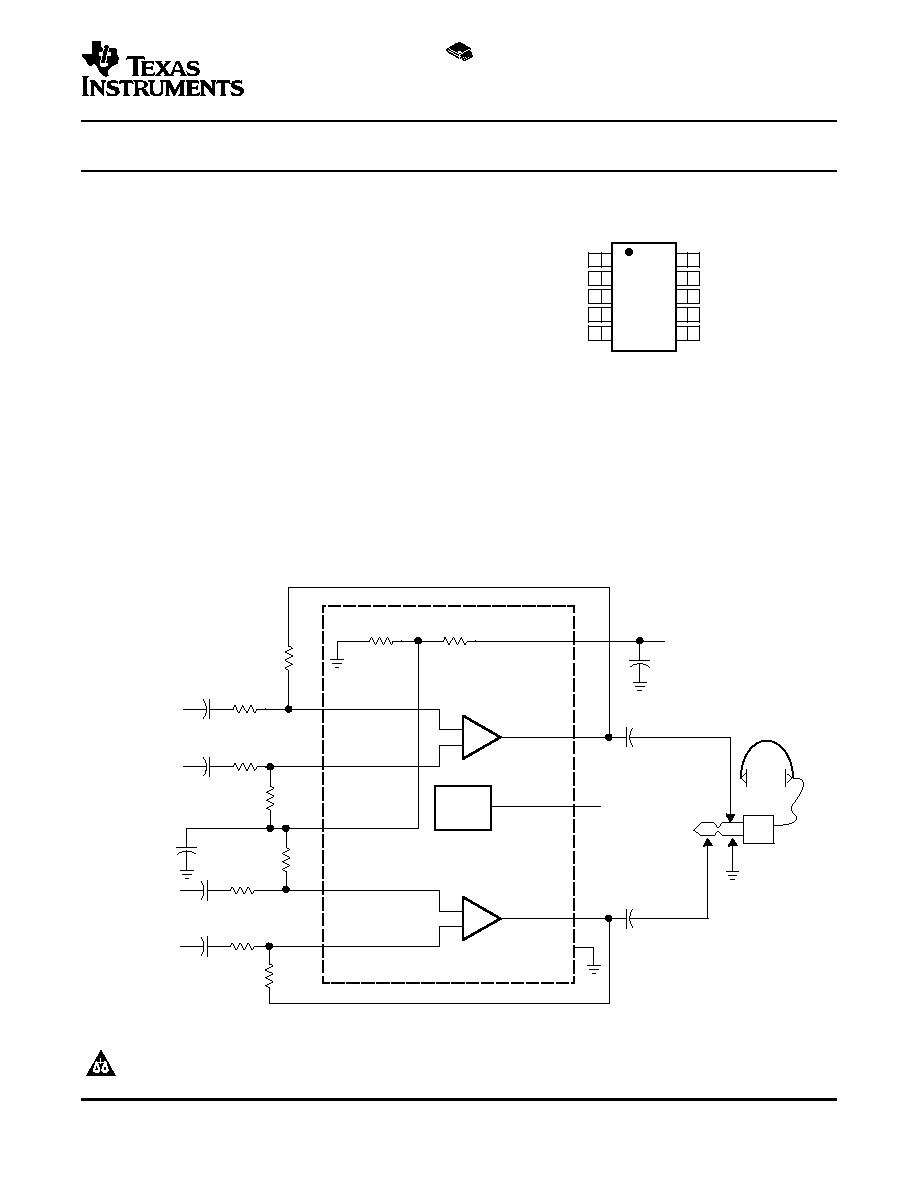
TYPICAL APPLICATION CIRCUIT
Right In
(Differential)
Bias
Control
10
1
9
5
V
O
1
V
O
2
V
DD
2
4
7
IN1≠
BYPASS
V
DD
/2
C
i
R
i
R
i
325 k
325 k
C
(B)
C
(S)
C
i
R
i
IN2+
R
f
V
DD
From
Shutdown
Control Circuit
≠
+
≠
+
C
(C)
C
(C)
3
IN1+
C
i
R
i
SHUTDOWN
R
f
8
C
i
R
i
IN2≠
R
f
6
≠
+
+
≠
Left In
(Differential)
TPA6112A2
SLOS342A ≠ DECEMBER 2000 ≠ REVISED SEPTEMBER 2004
150-mW STEREO AUDIO POWER AMPLIFIER
∑
150 mW Stereo Output
∑
Differential Inputs
∑
PC Power Supply Compatible
≠ Fully Specified for 3.3 V and 5 V Operation
≠ Operation to 2.5 V
∑
Pop Reduction Circuitry
∑
Internal Mid-Rail Generation
∑
Thermal and Short-Circuit Protection
∑
Surface-Mount Packaging
≠ PowerPADTM MSOP
The TPA6112A2 is a stereo audio power amplifier with differential inputs packaged in a 10-pin PowerPAD MSOP
package capable of delivering 150 mW of continuous RMS power per channel into 16-
loads. Amplifier gain is
externally configured by means of two resistors per input channel and does not require external compensation for
settings of 1 to 10.
Please be aware that an important notice concerning availability, standard warranty, and use in critical applications of Texas
Instruments semiconductor products and disclaimers thereto appears at the end of this data sheet.
PowerPAD is a trademark of Texas Instruments.
PRODUCTION DATA information is current as of publication date.
Copyright © 2000≠2004, Texas Instruments Incorporated
Products conform to specifications per the terms of the Texas
Instruments standard warranty. Production processing does not
necessarily include testing of all parameters.
www.ti.com
DESCRIPTION (CONTINUED)
ABSOLUTE MAXIMUM RATINGS
TPA6112A2
SLOS342A ≠ DECEMBER 2000 ≠ REVISED SEPTEMBER 2004
These devices have limited built-in ESD protection. The leads should be shorted together or the device
placed in conductive foam during storage or handling to prevent electrostatic damage to the MOS gates.
THD+N when driving an 16-
load from 5 V is 0.03% at 1 kHz, and less than 1% across the audio band of 20 Hz
to 20 kHz. For 32-
loads, the THD+N is reduced to less than 0.02% at 1 kHz, and is less than 1% across the
audio band of 20 Hz to 20 kHz. For 10-k
loads, the THD+N performance is 0.005% at 1 kHz, and less than
0.5% across the audio band of 20 Hz to 20 kHz.
AVAILABLE OPTIONS
PACKAGED DEVICE
T
A
MSOP SYMBOLIZATION
MSOP
(1)
-40
∞
C to 85
∞
C
TPA6112A2DGQ
TI APD
(1)
The DGQ package isavailable in left-ended tape and reel only (e.g., TPA6112A2DGQR).
Terminal Functions
TERMINAL
I/O
DESCRIPTION
NAME
NO
BYPASS
4
I
Tap to voltage divider for internal mid-supply bias supply. Connect to a 0.1 µF to 1 µF low ESR capacitor
for best performance.
GND
5
I
GND is the ground connection.
IN1-
2
I
IN1- is the negative input for channel 1.
IN1+
3
I
IN1+ is the positive input for channel 1.
IN2-
8
I
IN2- is the negative input for channel 2.
IN2+
7
I
IN2+ is the positive input for channel 2.
SHUTDOWN
6
I
Puts the device in a low quiescent current mode when held high.
V
DD
10
I
V
DD
is the supply voltage terminal.
V
O
1
1
O
V
O
1 is the audio output for channel 1.
V
O
2
9
O
V
O
2 is the audio output for channel 2.
over operating free-air temperature (unless otherwise noted
(1)
)
UNITS
V
DD
Supply voltage
6 V
V
I
Input voltage
-0.3 V to V
DD
+ 0.3 V
Continuous total power dissipation
internally limited
T
J
Operating junction temperature range
-40
∞
C to 150
∞
C
T
stg
Storage temperature range
-65
∞
C to 150
∞
C
Lead temperature 1,6 mm (1/16 inch) from case for 10 seconds
260
∞
C
(1)
Stresses beyond thoselisted under absolute maximum ratings may cause permanent damage to the device.These are stress ratings
only, and functional operation of the device at theseor any other conditions beyond those indicated under recommended
operatingconditions is not implied. Exposure to absolute-maximum-rated conditions forextended periods may affect device reliability.
2
www.ti.com
DISSIPATION RATING TABLE
RECOMMENDED OPERATING CONDITIONS
DC ELECTRICAL CHARACTERISTICS
AC OPERATING CHARACTERISTICS
DC ELECTRICAL CHARACTERISTICS
TPA6112A2
SLOS342A ≠ DECEMBER 2000 ≠ REVISED SEPTEMBER 2004
T
A
25
∞
C
DERATING FACTOR
T
A
= 70
∞
C
T
A
= 85
∞
C
PACKAGE
POWER RATING
ABOVE T
A
= 25
∞
C
POWER RATING
POWER RATING
DGQ
2.14 W
(1)
17.1 mW/
∞
C
1.37 W
1.11 W
(1)
Please see the Texas Instrumentsdocument, PowerPAD Thermally EnhancedPackage Application
Report (literature number SLMA002), for moreinformation on the PowerPAD package. The thermal
data was measured on a PCBlayout based on the information in the section entitledTexas
Instruments Recommended Board forPowerPAD on page 33 of the before mentioneddocument.
MIN
MAX
UNIT
V
DD
Supply voltage
2.5
5.5
V
T
A
Operating free-air temperature
-40
85
∞
C
V
IH
, (SHUTDOWN)
High-level input voltage
60% x V
DD
V
V
IL
, (SHUTDOWN)
Low-level input voltage
25% x V
DD
V
At T
A
= 25
∞
C, V
DD
= 2.5 V (Unless Otherwise Noted)
PARAMETER
TEST CONDITIONS
MIN
TYP
MAX
UNIT
V
OO
Output offset voltage
A
V
= 2 V/V
15
mV
PSRR
Power supply rejection ratio
V
DD
= 3.2 V to 3.4 V
83
dB
I
DD
Supply current
SHUTDOWN = 0 V
1.5
3
mA
I
DD(SD)
Supply current in SHUTDOWN mode
SHUTDOWN = V
DD
10
50
µA
Z
i
Input impedance
>1
M
V
DD
= 3.3 V, T
A
= 25
∞
C, R
L
= 16
PARAMETER
TEST CONDITIONS
MIN
TYP
MAX
UNIT
P
O
Output power (each channel)
THD
0.1%, f = 1 kHz
60
mW
THD+N
Total harmonic distortion + noise
P
O
= 40 mW, 20 - 20 kHz
0.4%
B
OM
Maximum output power BW
G = 10, THD < 5%
> 20
kHz
Phase margin
Open loop
96
∞
Supply ripple rejection ratio
f = 1 kHz
71
dB
Channel/channel output separation
f = 1 kHz
89
dB
SNR
Signal-to-noise ratio
P
O
= 50 mW, A
V
= 1
100
dB
V
n
Noise output voltage
A
V
= 1
11
µV(rms)
At T
A
= 25
∞
C, V
DD
= 5 .5 V (Unless otherwise noted)
PARAMETER
TEST CONDITIONS
MIN
TYP
MAX
UNIT
V
OO
Output offset voltage
A
V
= 2 V/V
15
mV
PSRR
Power supply rejection ratio
V
DD
= 4.9 V to 5.1 V
76
dB
I
DD
Supply current
SHUTDOWN = 0 V
1.5
3
mA
I
DD(SD)
Supply current in SHUTDOWN mode
SHUTDOWN = V
DD
60
100
µA
|I
IH
|
High-level input current (SHUTDOWN)
V
DD
= 5.5 V, V
I
= V
DD
1
µA
|I
IL
|
Low-level input current (SHUTDOWN)
V
DD
= 5.5 V, V
I
= 0 V
1
µA
Z
i
Input impedance
>1
M
3
www.ti.com
AC OPERATING CHARACTERISTICS
AC OPERATING CHARACTERISTICS
AC OPERATING CHARACTERISTICS
TPA6112A2
SLOS342A ≠ DECEMBER 2000 ≠ REVISED SEPTEMBER 2004
V
DD
= 5 V, T
A
= 25
∞
C, R
L
= 16
PARAMETER
TEST CONDITIONS
MIN
TYP
MAX
UNIT
P
O
Output power (each channel)
THD
0.1%, f = 1 kHz
150
mW
THD+N
Total harmonic distortion + noise
P
O
= 100 mW, 20 - 20 kHz
0.6%
B
OM
Maximum output power BW
G = 10, THD < 5%
> 20
kHz
Phase margin
Open loop
96
∞
Supply ripple rejection ratio
f = 1 kHz
61
dB
Channel/channel output separation
f = 1 kHz
90
dB
SNR
Signal-to-noise ratio
P
O
= 100 mW, A
V
= 1
100
dB
V
n
Noise output voltage
A
V
= 1
11.7
µV(rms)
V
DD
= 3.3 V, T
A
= 25
∞
C, R
L
= 32
PARAMETER
TEST CONDITIONS
MIN
TYP
MAX
UNIT
P
O
Output power (each channel)
THD
0.1%, f = 1 kHz
40
mW
THD+N
Total harmonic distortion + noise
P
O
= 30 mW, 20 - 20 kHz
0.4%
B
OM
Maximum output power BW
A
V
= 10, THD < 2%
> 20
kHz
Phase margin
Open loop
96
∞
Supply ripple rejection ratio
f = 1 kHz
71
dB
Channel/channel output separation
f = 1 kHz
95
dB
SNR
Signal-to-noise ratio
P
O
= 40 mW, A
V
= 1
100
dB
V
n
Noise output voltage
A
V
= 1
11
µV(rms)
V
DD
= 5 V, T
A
= 25
∞
C, R
L
= 32
PARAMETER
TEST CONDITIONS
MIN
TYP
MAX
UNIT
P
O
Output power (each channel)
THD
0.1%, f = 1 kHz
90
mW
THD+N
Total harmonic distortion + noise
P
O
= 60 mW, 20 - 20 kHz
0.4%
B
OM
Maximum output power BW
A
V
= 10, THD < 2%
> 20
kHz
Phase margin
Open loop
97
∞
Supply ripple rejection ratio
f = 1 kHz
61
dB
Channel/channel output separation
f = 1 kHz
98
dB
SNR
Signal-to-noise ratio
P
O
= 90 mW, A
V
= 1
100
dB
V
n
Noise output voltage
A
V
= 1
11.7
µV(rms)
4
www.ti.com
TYPICAL CHARACTERISTICS
0.001
10
0.01
0.1
1
20
20k
100
1k
10k
THD+N - T
otal Harmonic Distortion + Noise - %
f - Frequency - Hz
V
DD
= 3.3 V,
P
O
= 25 mW,
C
B
= 1
µ
F,
R
L
= 32
,
A
V
= -1 V/V
10
100
0.001
10
0.01
0.1
1
THD+N - T
otal Harmonic Distortion + Noise - %
V
DD
= 3.3 V,
R
L
= 32
,
A
V
= -1 V/V,
C
B
= 1
µ
F
50
P
O
- Output Power - mW
20 Hz
1 kHz
20 kHz
TPA6112A2
SLOS342A ≠ DECEMBER 2000 ≠ REVISED SEPTEMBER 2004
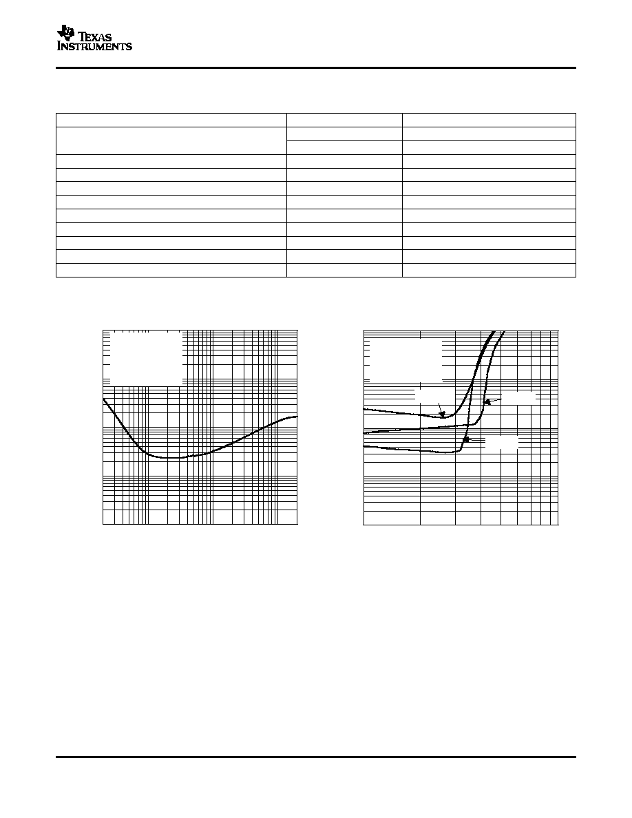
Table of Graphs
FIGURE
vs Frequency
1, 3, 5, 6, 7, 9, 11, 13,
THD+N
Total harmonic distortion plus noise
vs Output power
2, 4, 8, 10, 12, 14
Supply ripple rejection ratio
vs Frequency
15, 16
V
n
Output noise voltage
vs Frequency
17, 18
Crosstalk
vs Frequency
19 - 24
Shutdown attenuation
vs Frequency
25, 26
Open-loop gain and phase margin
vs Frequency
27, 28
Output power
vs Load resistance
29, 30,
I
DD
Supply current
vs Supply voltage
31
SNR
Signal-to-noise ratio
vs Voltage gain
32
Power dissipation/amplifier
vs Load power
33, 34
TOTAL HARMONIC DISTORTION + NOISE
TOTAL HARMONIC DISTORTION + NOISE
vs
vs
FREQUENCY
OUTPUT POWER
Figure 1.
Figure 2.
5