 | –≠–ª–µ–∫—Ç—Ä–æ–Ω–Ω—ã–π –∫–æ–º–ø–æ–Ω–µ–Ω—Ç: TPS2074 | –°–∫–∞—á–∞—Ç—å:  PDF PDF  ZIP ZIP |
TPS2074, TPS2075
FOUR-PORT USB HUB POWER CONTROLLERS
SLVS288A ≠ SEPTEMBER 2000 ≠ REVISED FEBRUARY 2001
1
POST OFFICE BOX 655303
∑
DALLAS, TEXAS 75265
D
Complete USB Hub Power Solution
D
Meets USB Specifications 1.1 and 2.0
D
Independent Thermal and Short-Circuit
Protection
D
3.3-V Regulator for USB Hub Controller
D
Overcurrent Logic Outputs
D
4.5-V to 5.5-V Operating Range
D
CMOS- and TTL-Compatible Enable Inputs
D
185
µ
A Bus-Power Supply Current
D
Available in 24-Pin SSOP Package
D
≠40
∞
C to 85
∞
C Ambient Temperature Range
description
The TPS2074 and TPS2075 provide a complete
USB hub power solution by incorporating three
major functions: current-limited power switches
for four ports, a 3.3-V 100-mA regulator, and a
DP0 line control to signal attach/detach of the hub.
These devices are designed to meet bus-pow-
ered and self-powered hub requirements. These
devices are also designed for hybrid hub
implementations and allow for automatic switch-
ing from self-powered mode to bus-powered
mode if loss of self-power is experienced. This
feature can be disabled by applying a logic high to
the BP_DIS input
Each port has a current-limited 100-m
N-
channel MOSFET high-side power switch for
500 mA self-powered operation. Each port also
has a current-limited 500-m
N-channel MOS-
FET high-side power switch for 100-mA bus-
powered operation. All the N-channel MOSFETs
are designed without parasitic diodes, preventing
current backflow into the inputs.
For applications where a 5-V regulator is needed,
use the TPS2070 or TPS2071 device.
SELECTION GUIDE
TA
USB HUB POWER CONTROLLERS
PACKAGED DEVICES
TA
USB HUB POWER CONTROLLERS
PIN COUNT
BPMODE
HTSSOP (DAP)
SSOP (DB)
Four port with internal LDO controller
32
Active low
TPS2070DAP
--
40
∞
C to 85
∞
C
Four-port with internal LDO controller
32
Active high
TPS2071DAP
--
≠ 40
∞
C to 85
∞
C
Four port without internal LDO controller
24
Active low
--
TPS2074DB
Four-port without internal LDO controller
24
Active high
--
TPS2075DB
The DB package is available taped and reeled. Add an R suffix to the device type (e.g., TPS2074DBR).
Copyright
2001, Texas Instruments Incorporated
PRODUCTION DATA information is current as of publication date.
Products conform to specifications per the terms of Texas Instruments
standard warranty. Production processing does not necessarily include
testing of all parameters.
Please be aware that an important notice concerning availability, standard warranty, and use in critical applications of
Texas Instruments semiconductor products and disclaimers thereto appears at the end of this data sheet.
NC ≠ No internal connection
Pin 9 is active low (BPMODE) for TPS2074
and active high (BPMODE) for TPS2075.
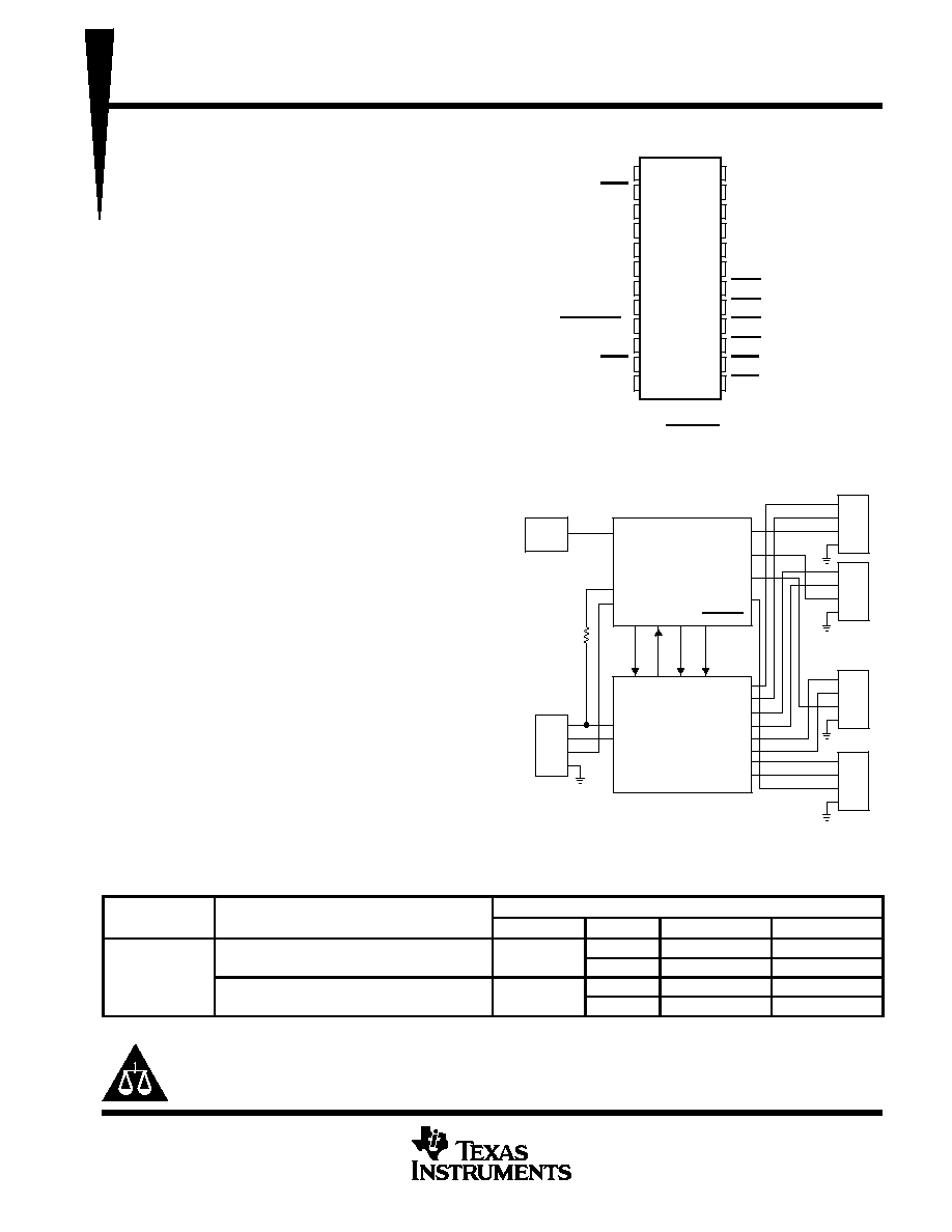
SP
DP0_RST
BP
DP0
DM0
Power
Supply
D+
D≠
5 V
GND
1.5
k
Upstream
Port
3.3 V_OUT
BPMODE
D+
D≠
5 V
GND
D+
D≠
5 V
GND
D+
D≠
5 V
GND
D+
D≠
5 V
GND
OUT1
OUT2
OUT3
OUT4
DP1
DM1
DP2
DM2
DP3
DM3
DP4
DM4
Downstream
Ports
TPS2074
Hub
Controller
VCC EN OC
simplified hybrid-hub diagram
See Figure 33 for complete implementation.
1
2
3
4
5
6
7
8
9
10
11
12
24
23
22
21
20
19
18
17
16
15
14
13
PG_DLY
EN1
AGND
PG
SP
SP
NC
3.3V_OUT
BPMODE
DP0_RST
EN2
DGND
BP_DIS
BP
OUT1
OUT2
OUT3
OUT4
OC4
OC3
OC2
OC1
EN4
EN3
DB PACKAGE
(TOP VIEW)

TPS2074, TPS2075
FOUR-PORT USB HUB POWER CONTROLLERS
SLVS288A ≠ SEPTEMBER 2000 ≠ REVISED FEBRUARY 2001
2
POST OFFICE BOX 655303
∑
DALLAS, TEXAS 75265
functional block diagram
3.3 V_OUT
3.3 V/100 mA LDO
S1
S2
S3
S4
S5
S6
S7
S8
BP
SP
SP
PG
PG_DLY
OUT1
OUT2
OUT3
OUT4
DPO_RST
BP_DIS
AGND
DGND
EN1
Control
Logic
OC1
EN2
OC2
EN3
OC3
EN4
OC4
BPMODE (TPS2074)
BPMODE (TPS2075)

TPS2074, TPS2075
FOUR-PORT USB HUB POWER CONTROLLERS
SLVS288A ≠ SEPTEMBER 2000 ≠ REVISED FEBRUARY 2001
3
POST OFFICE BOX 655303
∑
DALLAS, TEXAS 75265
Terminal Functions
TERMINAL
I/O
DESCRIPTION
NAME
NO.
I/O
DESCRIPTION
PG_DLY
1
Adjusts the PG time delay with a capacitor to ground. Adjust the pulse width to fit the application.
EN1
2
I
Active-low enable for OUT1
AGND
3
Analog ground
PG
4
O
Logic output, power good
SP
5
I
Self-power voltage input, connects to local power supply
SP
6
I
Self-power voltage input, connects to local power supply
NC
7
No internal connection
3.3V_OUT
8
O
3.3-V internal voltage regulator output
BPMODE
9
O
A logic signal that indicates if the outputs source from the bus-powered supply, BPMODE (TPS2074) or BPMODE
(TPS2075), can be used to signal the hub controller.
DP0_RST
10
O
Connects to DP signal from upstream hub/host through an external 1.5-k
resistor
EN2
11
I
Active-low enable for OUT2
DGND
12
Digital ground
EN3
13
I
Active-low enable for OUT3
EN4
14
I
Active-low enable for OUT4
OC1
15
O
Logic output, overcurrent response for OUT1
OC2
16
O
Logic output, overcurrent response for OUT2
OC3
17
O
Logic output, overcurrent response for OUT3
OC4
18
O
Logic output, overcurrent response for OUT4
OUT4
19
O
Power switch output for downstream ports
OUT3
20
O
Power switch output for downstream ports
OUT2
21
O
Power switch output for downstream ports
OUT1
22
O
Power switch output for downstream ports
BP
23
I
Bus power voltage input, connect to VBUS
BP_DIS
24
I
Active-high logic input, disables autoswitch to bus power when self power is disconnected. Connect to BP or GND
Use the following formula to calculate the capacitance needed;
C = (desired pulse width
◊
3
◊
10≠6 / 1.22
Pin 9 is active low for TPS2074 and active high for TPS2075.

TPS2074, TPS2075
FOUR-PORT USB HUB POWER CONTROLLERS
SLVS288A ≠ SEPTEMBER 2000 ≠ REVISED FEBRUARY 2001
4
POST OFFICE BOX 655303
∑
DALLAS, TEXAS 75265
detailed description
BP
The bus-powered supply input (BP) serves as the source for the internal 3.3-V LDO and for all logic functions
in the device. In bus-powered mode, BP also serves as the source for all the outputs (OUTx). If BP is below the
undervoltage threshold, all power switches will turn off and the LDO will be disabled. BP must be connected to
a voltage source in order for the device to operate.
SP
The self-powered supply input (SP) serves as the source for all the outputs (OUTx) in self-powered mode. The
enable logic for the SP switches requires that BP be connected to a voltage source.
OUT1, OUT2, OUT2, OUT4
OUTx are the outputs of the integrated power switches.
3.3V_OUT
The internal 3.3-V LDO output can be used to supply up to 100 mA current to low-power functions, such as hub
controllers.
DP0_RST
DP0_RST functions as a hub reset when a 1.5-k
resistor is connected between DP0_RST and the upstream
DP0 data line in a hub system. To provide a clean attach signal on DP0 data line, the DP0_RST output goes
low momentarily (because of the upstream pulldown resistor) to discharge any parasitic charge on the cable,
then goes to 3-state and finally outputs a high signal. The low and Hi-Z pulse widths are adjustable using a
capacitor between PG_DLY and ground, and are approximately 50% of the power-good time delay. Detachment
is signaled by a Hi-Z on DP0_RST. Both DP0_RST and PG will transition high at the same time.
Power Good (PG)
The power good (PG) function serves as a reset for a USB hub controller. PG is asserted low when the output
voltage on the internal voltage regulator is below a fixed threshold. A time delay to ensure a stable output voltage
before PG goes high is adjustable using a small-value ceramic capacitor from PG_DLY to ground.
PG_DLY
PG_DLY connects to an external capacitor to adjust the time delay for PG and DP0_RST. For USB applications,
a 0.1
µ
F capacitor is recommended, however, reference the USB hub controller data sheet to determine the
needed pulse width criteria.
BP_DIS
BP_DIS is used to enable or disable the autoswitching function between bus-powered mode and self-powered
mode. When BP_DIS is connected low and the voltage on SP is greater than the undervoltage-lockout (UVLO)
threshold, the device will switch to self-powered operation automatically; if the SP voltage falls lower than the
UVLO threshold, the device will switch to bus-powered operation. When BP_DIS is connected high, the
autoswitching function is disabled and the device will not autoswitch to bus-powered operation if the SP voltage
is below the UVLO threshold.
BPMODE or BPMODE
BPMODE (TPS2074) or BPMODE (TPS2075) is an output that signals when the device is in bus-powered
mode. The logic state is set according to the voltages on BP, SP, and BP_DIS. For the TPS2074, BPMODE
outputs a low signal to indicate bus-powered mode or a high signal to indicate self-powered mode. For the
TPS2075, BPMODE outputs a high signal to indicate bus-powered mode or a low signal to indicate self-powered
mode. This output can be used to inform a USB hub controller to configure for bus-powered mode or
self-powered mode.

TPS2074, TPS2075
FOUR-PORT USB HUB POWER CONTROLLERS
SLVS288A ≠ SEPTEMBER 2000 ≠ REVISED FEBRUARY 2001
5
POST OFFICE BOX 655303
∑
DALLAS, TEXAS 75265
detailed description (continued)
OC1, OC2, OC3, OC4
OCx is an output signal that is asserted (active low) when an overcurrent or overtemperature condition is
encountered for the corresponding channel. OCx will remain asserted until the overcurrent or overtemperature
condition is removed.
EN1, EN2, EN3, EN4,
The active-low logic input ENx enables or disables the power switches in the device. The enable input is
compatible with both TTL and CMOS logic levels. The switches will not turn on until 3.3V_OUT is above the PG
threshold.
absolute maximum ratings over operating free-air temperature range (unless otherwise noted)
Input voltage range: V
I(BP)
, V
I(SP)
, V
I(ENx)
, V
I(BP_DIS)
≠0.3 V to 6 V
. . . . . . . . . . . . . . . . . . . . . . . . . . . . . . . . .
Output voltage range: V
O(OUTx)
≠0.3 V to 6 V
. . . . . . . . . . . . . . . . . . . . . . . . . . . . . . . . . . . . . . . . . . . . . . . . . . . . .
V
O(3.3V_OUT)
, V
O(PG_DLY)
, V
O(OCx)
, V
O(BPMODE)
,
V
O(DP0_RST)
, V
O(PG)
≠0.3 V to V
O
(3.3V_OUT)
0.3 V
. . . . . . . . . . . . . . . . . . . . . . . . . . .
Continuous output current: I
O(OUTx)
, I
O(3.3V_OUT)
internally limited
. . . . . . . . . . . . . . . . . . . . . . . . . . . . . . . . . .
Maximum output current:
I
O(BPMODE)
or I
O(BPMODE)
, I
O(DP0_RST)
, I
O(PG)
, I
O(OCx)
±
10 mA
. . . . . . . . . .
Continuous total power dissipation
See Dissipation Rating Table
. . . . . . . . . . . . . . . . . . . . . . . . . . . . . . . . . . . . . .
Operating virtual junction temperature range, T
J
≠40
∞
C to 125
∞
C
. . . . . . . . . . . . . . . . . . . . . . . . . . . . . . . . . . . . . .
Storage temperature range, T
stg
≠65
∞
C to 150
∞
C
. . . . . . . . . . . . . . . . . . . . . . . . . . . . . . . . . . . . . . . . . . . . . . . . . . . .
Lead temperature soldering 1,6 mm (1/16 inch) from case for 10 seconds
260
∞
C
. . . . . . . . . . . . . . . . . . . . . . .
Stresses beyond those listed under "absolute maximum ratings" may cause permanent damage to the device. These are stress ratings only, and
functional operation of the device at these or any other conditions beyond those indicated under "recommended operating conditions" is not
implied. Exposure to absolute-maximum-rated conditions for extended periods may affect device reliability.
All voltages are with respect to GND.
DISSIPATION RATING TABLE
PACKAGE
TA
25
∞
C
POWER RATING
DERATING FACTOR
ABOVE TA = 25
∞
C
TA = 70
∞
C
POWER RATING
TA = 85
∞
C
POWER RATING
24 DB
889.7 mW
8.9 mW/
∞
C
489.3 mW
355.9 mW
recommended operating conditions
MIN
MAX
UNIT
VI(BP)
4.5
5.5
Input voltage
VI(SP)
0
5.5
V
Input voltage
VI(BP_DIS)
0
5.5
V
VI(ENx)
0
5.5
BP to OUTx (per switch)
100
Continuous output current, IO SP to OUTx (per switch)
500
mA
O
BP to 3.3V_OUT
100
Operating virtual junction temperature, TJ
-40
125
∞
C