 | –≠–ª–µ–∫—Ç—Ä–æ–Ω–Ω—ã–π –∫–æ–º–ø–æ–Ω–µ–Ω—Ç: TPS2081 | –°–∫–∞—á–∞—Ç—å:  PDF PDF  ZIP ZIP |
TPS2080, TPS2081, TPS2082 DUAL,
TPS2085, TPS2086, TPS2087 QUAD
POWER DISTRIBUTION SWITCHES
SLVS202A - SEPTEMBER 2000 - REVISED MARCH 2001
1
WWW.TI.COM
D
80-m
High-Side MOSFET Switch
D
500 mA Continuous Current per Channel
D
Independent Thermal and Short-Circuit
Protection With Overcurrent Logic Output
D
Operating Range . . . 2.7-V to 5.5-V
D
CMOS- and TTL-Compatible Enable Inputs
D
2.5-ms Typical Rise Time
D
Undervoltage Lockout
D
10
µ
A Maximum Standby Supply Current
D
Bidirectional Switch
D
Available in 8-Pin and 16-Pin SOIC
Packages
D
Ambient Temperature Range, 0
∞
C to 85
∞
C
D
ESD Protection
description
The TPS2080, TPS2081, and TPS2082 dual and
the TPS2085, TPS2086 and TPS2087 quad
power-distribution switches are intended for
applications where heavy capacitive loads and
short circuits are likely to be encountered. The
TPS208x devices incorporate 80-m
N-channel
MOSFET high-side power switches for power-distribution systems that require multiple power switches in a
single package. Each switch is controlled by an independent logic enable input. Gate drive is provided by an
internal charge pump designed to control the power-switch rise times and fall times to minimize current surges
during switching. The charge pump requires no external components and allows operation from supplies as low
as 2.7 V.
When the output load exceeds the current-limit threshold or a short is present, the TPS208x limits the output
current to a safe level by switching into a constant-current mode, pulling the overcurrent (OCx) logic output low.
When continuous heavy overloads and short circuits increase the power dissipation in the switch causing the
junction temperature to rise, a thermal protection circuit shuts off the switch to prevent damage. Recovery from
a thermal shutdown is automatic once the device has cooled sufficiently. Internal circuitry ensures the switch
remains off until valid input voltage is present. The TPS208x devices are designed to current limit at
1.0-A load.
TPS201xA
TPS202x
TPS203x
33 m
, single
0.2 A - 2 A
0.2 A - 2 A
0.2 A - 2 A
TPS2014
TPS2015
TPS2041
TPS2051
TPS2045
TPS2055
80 m
, single
600 mA
1 A
500 mA
500 mA
250 mA
250 mA
GENERAL SWITCH CATALOG
TPS2042
TPS2052
TPS2046
TPS2056
80 m
, dual
500 mA
500 mA
250 mA
250 mA
TPS2100/1
260 m
IN1 500 mA
IN2 10 mA
OUT
IN1
IN2
TPS2102/3/4/5
IN1 500 mA
IN2 100 mA
1.3
TPS2043
TPS2053
TPS2047
TPS2057
80 m
, triple
500 mA
500 mA
250 mA
250 mA
TPS2044
TPS2054
TPS2048
TPS2058
80 m
, quad
500 mA
500 mA
250 mA
250 mA
80 m
, dual
TPS2080
TPS2081
TPS2082
TPS2090
500 mA
500 mA
500 mA
250 mA
TPS2091
TPS2092
250 mA
250 mA
80 m
, quad
TPS2085
TPS2086
TPS2087
TPS2095
500 mA
500 mA
500 mA
250 mA
TPS2096
TPS2097
250 mA
250 mA
Copyright
2001, Texas Instruments Incorporated
PRODUCTION DATA information is current as of publication date.
Products conform to specifications per the terms of Texas Instruments
standard warranty. Production processing does not necessarily include
testing of all parameters.
Please be aware that an important notice concerning availability, standard warranty, and use in critical applications of
Texas Instruments semiconductor products and disclaimers thereto appears at the end of this data sheet.
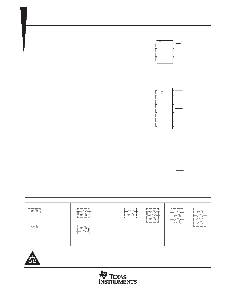
1
2
3
4
8
7
6
5
GND
IN1
IN2
EN1
OC
OUT1
OUT2
EN2
TPS2080, TPS2081, AND TPS2082
D PACKAGE
1
2
3
4
5
6
7
8
16
15
14
13
12
11
10
9
GNDA
IN1
IN2
EN1
GNDB
IN3
IN4
EN3
OCA
OUT1
OUT2
EN2
OCB
OUT3
OUT4
EN4
TPS2085, TPS2086 AND TPS2087
D PACKAGE
(TOP VIEW)
See Available Options table
See Available Options table
(TOP VIEW)
TPS2080, TPS2081, TPS2082 DUAL,
TPS2085, TPS2086, TPS2087 QUAD
POWER DISTRIBUTION SWITCHES
SLVS202A - SEPTEMBER 2000 - REVISED MARCH 2001
2
WWW.TI.COM
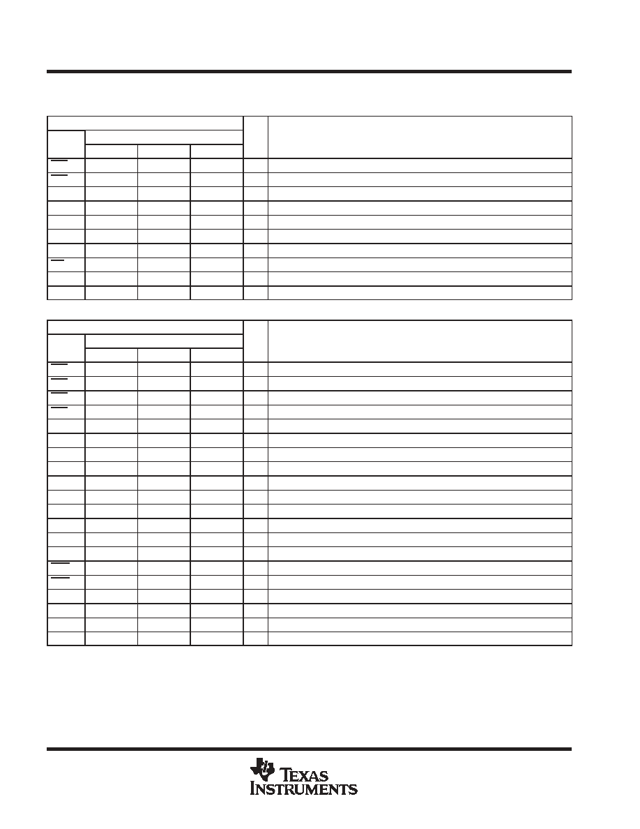
AVAILABLE OPTIONS
DUAL POWER DISTRIBUTION SWITCHES
TA
ENABLE
RECOMMENDED
MAXIMUM
CONTINUOUS
TYPICAL
SHORT-CIRCUIT
CURRENT LIMIT
PACKAGED
DEVICES
TA
EN1
EN2
CONTINUOUS
LOAD CURRENT
(A)
CURRENT LIMIT
AT 25
∞
C
(A)
SMALL OUTLINE
(D)
Active high
Active high
TPS2080D
0
∞
C to 85
∞
C
Active high
Active low
0.5
1.0
TPS2081D
0 C to 85 C
Active low
Active low
0.5
1.0
TPS2082D
QUAD POWER DISTRIBUTION SWITCHES
TA
ENABLE
RECOMMENDED
MAXIMUM
CONTINUOUS
TYPICAL
SHORT-CIRCUIT
CURRENT LIMIT
PACKAGED
DEVICES
TA
EN1
EN2
EN3
EN4
CONTINUOUS
LOAD CURRENT
(A)
CURRENT LIMIT
AT 25
∞
C
(A)
SMALL OUTLINE
(D)
Active high
Active high
Active high
Active high
TPS2085D
0
∞
C to 85
∞
C
Active high
Active low
Active high
Active low
0.5
1.0
TPS2086D
0 C to 85 C
Active low
Active low
Active low
Active low
0.5
1.0
TPS2087D
The D package is available taped and reeled. Add an R suffix to device type (e.g., TPS2081DR)
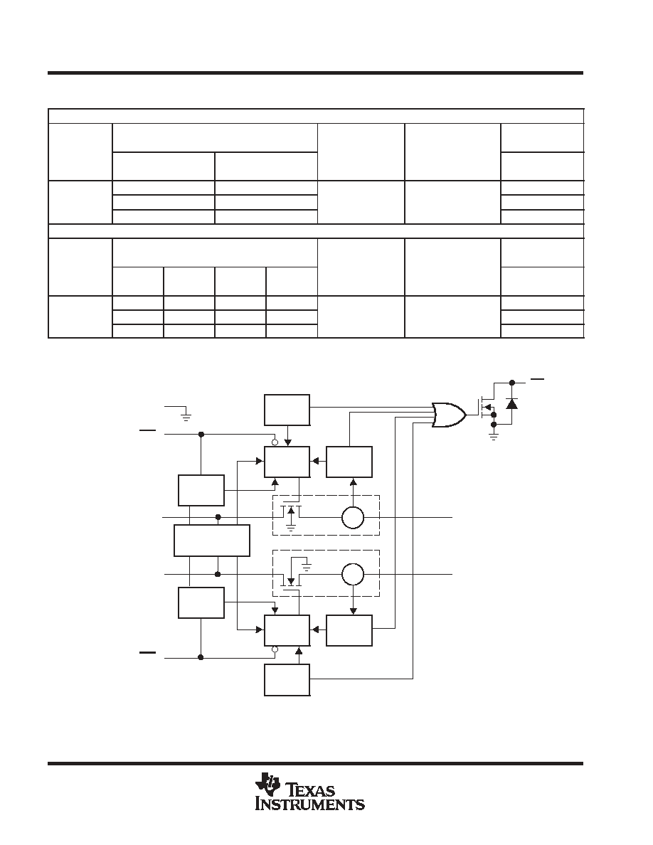
TPS2082 functional block diagram
Current sense
Thermal
Sense
Driver
Current
Limit
Charge
Pump
VCC Select
and UVLO
CS
Driver
Current
Limit
CS
Thermal
Sense
Charge
Pump
Power Switch
GND
EN1
IN2
EN2ß
OC
OUT1
OUT2
IN1
Active high for TPS2080 and TPS2081
ß Active high for TPS2080
TPS2080, TPS2081, TPS2082 DUAL,
TPS2085, TPS2086, TPS2087 QUAD
POWER DISTRIBUTION SWITCHES
SLVS202A - SEPTEMBER 2000 - REVISED MARCH 2001
3
WWW.TI.COM
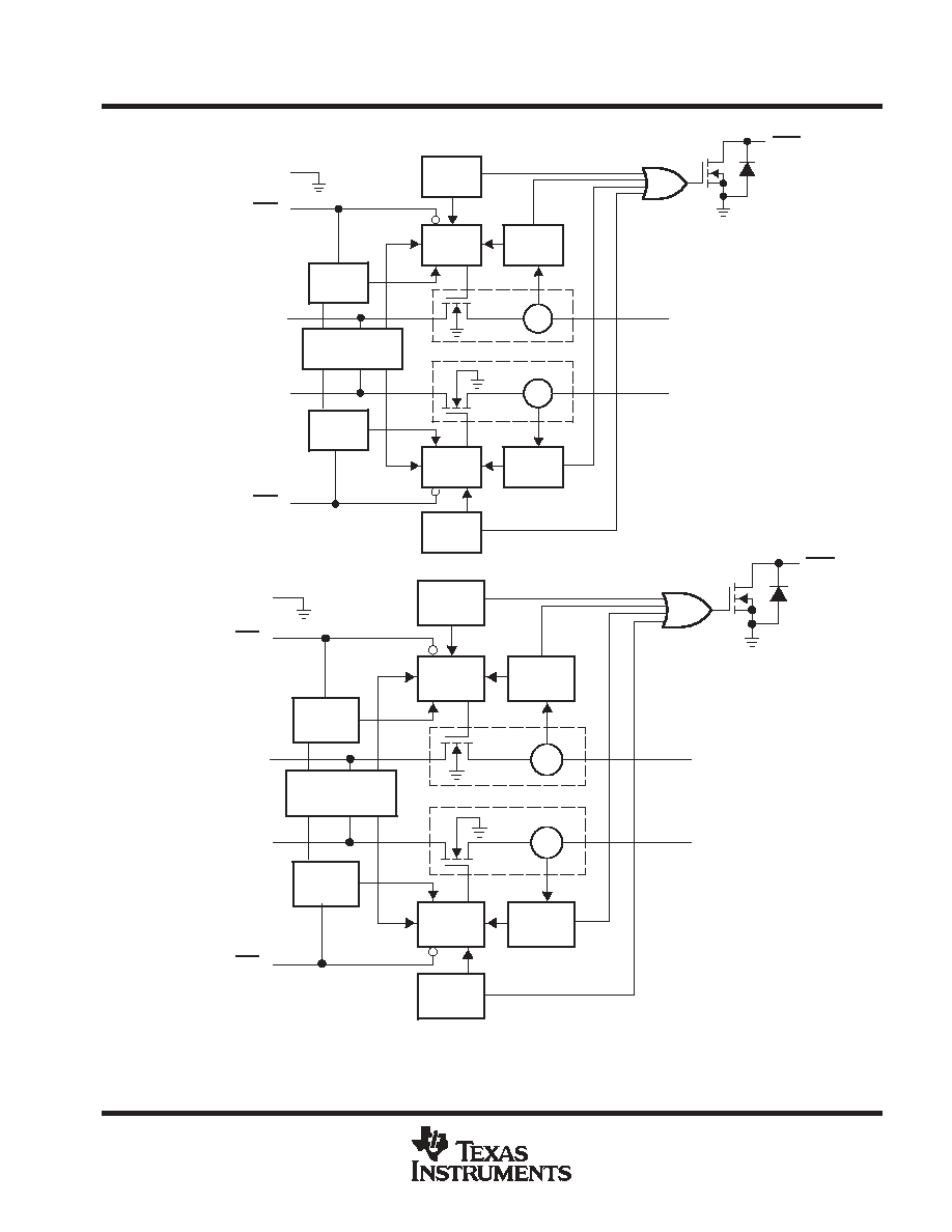
TPS2087 functional block diagram
Thermal
Sense
Driver
Current
Limit
Charge
Pump
VCC Select
and UVLO
CS
Driver
Current
Limit
CS
Thermal
Sense
Charge
Pump
Power Switch
GNDA
EN1
IN2
EN2ß
OCA
OUT1
OUT2
IN1
Current sense
Thermal
Sense
Driver
Current
Limit
Charge
Pump
VCC Select
and UVLO
CS
Driver
Current
Limit
CS
Thermal
Sense
Charge
Pump
Power Switch
GNDB
EN3
IN4
EN4ß
OCB
OUT3
OUT4
IN3
Active high for TPS2085 and TPS2086
ß Active high for TPS2085
TPS2080, TPS2081, TPS2082 DUAL,
TPS2085, TPS2086, TPS2087 QUAD
POWER DISTRIBUTION SWITCHES
SLVS202A - SEPTEMBER 2000 - REVISED MARCH 2001
4
WWW.TI.COM
Terminal Functions
DUAL POWER-DISTRIBUTION SWITCHES
TERMINAL
NAME
NO.
I/O
DESCRIPTION
NAME
TPS2080
TPS2081
TPS2082
I/O
DESCRIPTION
EN1
4
I
Enable input. Active low turns on power switch.
EN2
5
5
I
Enable input. Active low turns on power switch.
EN1
4
4
I
Enable input. Active high turns on power switch.
EN2
5
I
Enable input. Active high turns on power switch.
GND
1
1
1
I
Ground
IN1
2
2
2
I
N-Channel MOSFET Drain
IN2
3
3
3
I
N-Channel MOSFET Drain
OC
8
8
8
O
Overcurrent. Open drain output active low
OUT1
7
7
7
O
Power-switch output
OUT2
6
6
6
O
Power-switch output
QUAD POWER-DISTRIBUTION SWITCHES
TERMINAL
NAME
NO.
I/O
DESCRIPTION
NAME
TPS2085
TPS2086
TPS2087
I/O
DESCRIPTION
EN1
4
I
Enable input. Active low turns on power switch.
EN2
13
13
I
Enable input. Active low turns on power switch.
EN3
8
I
Enable input. Active low turns on power switch.
EN4
9
9
I
Enable input. Active low turns on power switch.
EN1
4
4
I
Enable input. Active high turns on power switch.
EN2
13
I
Enable input. Active high turns on power switch.
EN3
8
8
I
Enable input. Active high turns on power switch.
EN4
9
I
Enable input. Active high turns on power switch.
GNDA
1
1
1
Ground for IN1 and IN2 switch and circuitry
GNDB
5
5
5
Ground for IN3 and IN4 switch and circuitry
IN1
2
2
2
I
N-channel MOSFET drain
IN2
3
3
3
I
N-channel MOSFET drain
IN3
6
6
6
I
N-channel MOSFET drain
IN4
7
7
7
I
N-channel MOSFET drain
OCA
16
16
16
O
Overcurrent indicator for switch 1 and switch 2. Active-low open drain output.
OCB
12
12
12
O
Overcurrent indicator for switch 3 and switch 4. Active low open drain output
OUT1
15
15
15
O
Power-switch output
OUT2
14
14
14
O
Power-switch output
OUT3
11
11
11
O
Power-switch output
OUT4
10
10
10
O
Power-switch output

TPS2080, TPS2081, TPS2082 DUAL,
TPS2085, TPS2086, TPS2087 QUAD
POWER DISTRIBUTION SWITCHES
SLVS202A - SEPTEMBER 2000 - REVISED MARCH 2001
5
WWW.TI.COM
detailed description
power switch
The power switch is an N-channel MOSFET with a maximum on-state resistance of 135 m
(V
I(IN)
= 5 V).
Configured as a high-side switch, the power switch prevents current flow from OUTx to IN and IN to OUTx when
disabled. The power switch supplies a minimum of 500 mA per switch.
charge pump
An internal charge pump supplies power to the driver circuit and provides the necessary voltage to pull the gate
of the MOSFET above the source. The charge pump operates from input voltages as low as 2.7 V and requires
very little supply current.
driver
The driver controls the gate voltage of the power switch. To limit large current surges and reduce the associated
electromagnetic interference (EMI) produced, the driver incorporates circuitry that controls the rise times and
fall times of the output voltage. The rise and fall times are typically in the 2-ms to 4-ms range.
enable (ENx or ENx)
The logic enable disables the power switch and the bias for the charge pump, driver, and other circuitry to reduce
the supply current to less than 10
µ
A when a logic high is present on ENx or a logic low is present on ENx. A
logic low input on ENx or logic high on ENx restores bias to the drive and control circuits and turns the power
on. The enable input is compatible with both TTL and CMOS logic levels.
overcurrent (OCx)
The OCx open drain output is asserted (active low) when an overcurrent or over temperature condition is
encountered. The output will remain asserted until the overcurrent or overtemperature condition is removed.
current sense
A sense FET monitors the current supplied to the load. The sense FET measures current more efficiently than
conventional resistance methods. When an overload or short circuit is encountered, the current-sense circuitry
sends a control signal to the driver. The driver in turn reduces the gate voltage and drives the power FET into
its saturation region, which switches the output into a constant current mode and holds the current constant
while varying the voltage on the load.
thermal sense
The TPS208x implements a dual thermal trip to allow fully independent operation of the power distribution
switches. In an overcurrent or short-circuit condition the junction temperature rises. When the die temperature
rises to approximately 140
∞
C, the internal thermal sense circuitry checks to determine which power switch is
in an overcurrent condition and turns off that switch, thus isolating the fault without interrupting operation of the
adjacent power switch. Hysteresis is built into the thermal sense, and after the device has cooled approximately
20 degrees, the switch turns back on. The switch continues to cycle off and on until the fault is removed. The
(OCx) open-drain output is asserted (active low) when overtemperature or overcurrent occurs.
undervoltage lockout
A voltage sense circuit monitors the input voltage. When the input voltage is below approximately 2 V, a control
signal turns off the power switch.