TPS2100, TPS2101
V
AUX
POWER-DISTRIBUTION SWITCHES
SLVS197C ≠ JUNE 1999 ≠ REVISED APRIL 2000
1
POST OFFICE BOX 655303
∑
DALLAS, TEXAS 75265
features
D
Dual-Input, Single-Output MOSFET Switch
With No Reverse Current Flow (No Parasitic
Diodes)
D
IN1 . . . 250-m
, 500-mA N-Channel;
16-
Ķ
A Max Supply Current
D
IN2 . . . 1.3-
, 10-mA P-Channel;
1.5-
Ķ
A Max Supply Current (V
AUX
Mode)
D
Advanced Switch Control Logic
D
CMOS- and TTL-Compatible Enable Input
D
Controlled Rise, Fall, and Transition Times
D
2.7-V to 4 V Operating Range
D
SOT-23-5 and SOIC-8 Package
D
≠ 40
į
C to 70
į
C Ambient Temperature Range
D
2-kV Human-Body-Model, 750-V CDM,
200-V Machine-Model Electrostatic-
Discharge Protection
typical applications
D
Notebook and Desktop PCs
D
Palmtops and PDAs
description
The TPS2100 and TPS2101 are dual-input, single-output power switches designed to provide uninterrupted
output voltage when transitioning between two independent power supplies. Both devices combine one
n-channel (250 m
) and one p-channel (1.3
) MOSFET with a single output. The p-channel MOSFET (IN2)
is used with auxiliary power supplies that deliver lower current for standby modes. The n-channel MOSFET
(IN1) is used with a main power supply that delivers higher current required for normal operation. Low
on-resistance makes the n-channel the ideal path for higher main supply current when power-supply regulation
and system voltage drops are critical. When using the p-channel MOSFET, quiescent current is reduced to
0.75
Ķ
A to decrease the demand on the standby power supply. The MOSFETs in the TPS2100 and TPS2101
do not have the parasitic diodes, found in discrete MOSFETs, which allow the devices to prevent back-flow
current when the switch is off.
DBV PACKAGE
(TOP VIEW)
GND
IN2
IN1
OUT
EN
GND
IN2
IN1
OUT
EN
DBV PACKAGE
(TOP VIEW)
TPS2100
TPS2101
NC ≠ No internal connection
Figure 2. V
AUX
CardBus Implementation
PCI12xx / PCI14xx
CardBus Controller
PCI Bus
VAUX
3.3 V
VGA
TPS210x
VCC
D3-STAT
1
2
3
4
8
7
6
5
IN2
GND
EN
NC
OUT
OUT
NC
IN1
D PACKAGE
(TOP VIEW)
D PACKAGE
(TOP VIEW)
1
2
3
4
8
7
6
5
IN2
GND
EN
NC
OUT
OUT
NC
IN1
1
2
3
5
4
1
2
3
5
4
Copyright
©
2000, Texas Instruments Incorporated
PRODUCTION DATA information is current as of publication date.
Products conform to specifications per the terms of Texas Instruments
standard warranty. Production processing does not necessarily include
testing of all parameters.
Please be aware that an important notice concerning availability, standard warranty, and use in critical applications of
Texas Instruments semiconductor products and disclaimers thereto appears at the end of this data sheet.
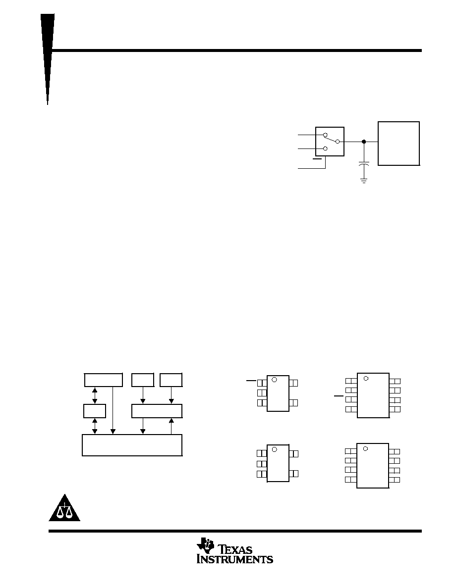
Figure 1. Typical Dual-Input Single-Output
Application
TPS2100
IN1
IN2
EN
3.3 V VCC
3.3 V VAUX
D3 or PME Status
Control Signal
Hold-Up
Capacitor
Controller
(CardBus,
1394,
PCI,
et al.)
3.3 V
TPS2100, TPS2101
V
AUX
POWER-DISTRIBUTION SWITCHES
SLVS197C ≠ JUNE 1999 ≠ REVISED APRIL 2000
3
POST OFFICE BOX 655303
∑
DALLAS, TEXAS 75265
Function Tables
TPS2100
TPS2101
VIN1
VIN2
EN
OUT
VIN1
VIN2
EN
OUT
0 V
0 V
XX
GND
0 V
0 V
XX
GND
0 V
3.3 V
L
GND
0 V
3.3 V
H
GND
3.3 V
3.3 V
L
VIN1
3.3 V
3.3 V
H
VIN1
3.3 V
0 V
L
VIN1
3.3 V
0 V
H
VIN1
0 V
3.3 V
H
VIN2
0 V
3.3 V
L
VIN2
3.3 V
0 V
H
VIN2
3.3 V
0 V
L
VIN2
3.3 V
3.3 V
H
VIN2
3.3 V
3.3 V
L
VIN2
XX = don't care
Terminal Functions
TERMINAL
NO.
DESCRIPTION
NAME
TPS2100
TPS2101
I/O
DESCRIPTION
DBV
D
DBV
D
EN
1
3
Active-high enable for IN1-OUT switch
EN
1
3
I
Active-low enable for IN1-OUT switch
GND
2
2
2
2
I
Ground
IN1
5
5
5
5
I
Main Input voltage, NMOS drain (250 m
)
IN2
3
1
3
1
I
Auxilliary input voltage, PMOS drain (1.3
)
OUT
4
7, 8
4
7, 8
O
Power switch output
NC
4, 6
4, 6
No connection
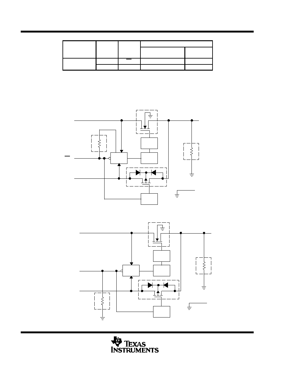
detailed description
power switches
n-channel MOSFET
The IN1-OUT n-channel MOSFET power switch has a typical on-resistance of 250 m
at 3.3-V input voltage,
and is configured as a high-side switch.
p-channel MOSFET
The IN2-OUT p-channel MOSFET power switch with typical on-resistance of 1.3
at 3.3-V input voltage and
is configured as a high-side switch. When operating, the p-channel MOSFET quiescent current is reduced to
less than 1.5
Ķ
A.
charge pump
An internal charge pump supplies power to the driver circuit and provides the necessary voltage to pull the gate
of the MOSFET above the source. The charge pump operates from input voltages as low as 2.7 V and requires
very little supply current.
driver
The driver controls the gate voltage of the IN1-OUT and IN2-OUT power switches. To limit large current surges
and reduce the associated electromagnetic interference (EMI) produced, the drivers incorporate circuitry that
controls the rise times and fall times of the output voltage.
TPS2100, TPS2101
V
AUX
POWER-DISTRIBUTION SWITCHES
SLVS197C ≠ JUNE 1999 ≠ REVISED APRIL 2000
4
POST OFFICE BOX 655303
∑
DALLAS, TEXAS 75265
detailed description (continued)
enable
The logic enable will turn on the IN2-OUT power switch when a logic high is present on EN (TPS2100) or logic
low is present on EN (TPS2101). A logic low input on EN (TPS2100) or logic high on EN (TPS2101) restores
bias to the drive and control circuits and turns on the IN1-OUT power switch. The enable input is compatible
with both TTL and CMOS logic levels.
the V
AUX
application for CardBus controllers
The PC Card specification requires the support of V
AUX
to the CardBus controller as well as to the PC Card
sockets. Both are 3.3-V requirements; however the CardBus controller's current demand from the V
AUX
supply
is limited to 10
Ķ
A, whereas the PC Card may consume as much as 200 mA. In either implementation, if support
of a wake-up event is required, the controller and the socket will transition from the 3.3-V V
CC
rail to the 3.3-V
V
AUX
rail when the equipment moves into a low power mode such as D3. The transition from V
CC
to V
AUX
needs
to be seamless in order to maintain all memory and register information in the system. If V
AUX
is not supported,
the system will lose all register information when it transitions to the D3 state.
absolute maximum ratings over operating free-air temperature (unless otherwise noted)
Input voltage range, V
I(IN1)
(see Note1)
≠ 0.3 V to 5 V
. . . . . . . . . . . . . . . . . . . . . . . . . . . . . . . . . . . . . . . . . . . . . . .
Input voltage range, V
I(IN2)
(see Note1)
≠ 0.3 V to 5 V
. . . . . . . . . . . . . . . . . . . . . . . . . . . . . . . . . . . . . . . . . . . . . . .
Input voltage range, V
I
at EN or EN
≠ 0.3 V to 5 V
. . . . . . . . . . . . . . . . . . . . . . . . . . . . . . . . . . . . . . . . . . . . . . . . . .
Output voltage range, V
O
(see Note 1)
≠ 0.3 V to 5 V
. . . . . . . . . . . . . . . . . . . . . . . . . . . . . . . . . . . . . . . . . . . . . . .
Continuous output current, I
O(IN1
) 700
mA
. . . . . . . . . . . . . . . . . . . . . . . . . . . . . . . . . . . . . . . . . . . . . . . . . . . . . . . .
Continuous output current, I
O(IN2)
70 mA
. . . . . . . . . . . . . . . . . . . . . . . . . . . . . . . . . . . . . . . . . . . . . . . . . . . . . . . . .
Continuous total power dissipation
See dissipation rating table
. . . . . . . . . . . . . . . . . . . . . . . . . . . . . . . . . . . . . . .
Operating virtual junction temperature range, T
J
≠ 40
į
C to 85
į
C
. . . . . . . . . . . . . . . . . . . . . . . . . . . . . . . . . . . . . .
Storage temperature range, T
stg
≠ 65
į
C to 150
į
C
. . . . . . . . . . . . . . . . . . . . . . . . . . . . . . . . . . . . . . . . . . . . . . . . . . .
Lead temperature soldering 1,6 mm (1/16 inch) from case for 10 seconds
260
į
C
. . . . . . . . . . . . . . . . . . . . . . .
Electrostatic discharge (ESD) protection: Human body model
2 kV
. . . . . . . . . . . . . . . . . . . . . . . . . . . . . . . . . . .
Machine model
200 V
. . . . . . . . . . . . . . . . . . . . . . . . . . . . . . . . . . . . . .
Charged device model (CDM)
750 V
. . . . . . . . . . . . . . . . . . . . . . . . .
Stresses beyond those listed under "absolute maximum ratings" may cause permanent damage to the device. These are stress ratings only, and
functional operation of the device at these or any other conditions beyond those indicated under "recommended operating conditions" is not
implied. Exposure to absolute-maximum-rated conditions for extended periods may affect device reliability.
NOTE 1: All voltages are with respect to GND.
DISSIPATION RATING TABLE
PACKAGE
TA < 25
į
C
POWER RATING
DERATING FACTOR
ABOVE TA = 25
į
C
TA = 70
į
C
POWER RATING
TA = 85
į
C
POWER RATING
DBV
309 mW
3.1 mW/
į
C
170 mW
123 mW
D
568 mW
5.7 mW/
į
C
313 mW
227 mW
recommended operating conditions
MIN
MAX
UNIT
Input voltage, VI(INx)
2.7
4
V
Input voltage, VI at EN and EN
0
4
V
Continuous output current, IO(IN1)
500
mA
Continuous output current, IO(IN2)
100
mA
Operating virtual junction temperature, TJ
≠ 40
85
į
C
The device can deliver up to 220 mA at IO(IN2). However, operation at the higher current levels will result in greater voltage drop across the device,
and greater voltage droop when switching between IN1 and IN2.