 | –≠–ª–µ–∫—Ç—Ä–æ–Ω–Ω—ã–π –∫–æ–º–ø–æ–Ω–µ–Ω—Ç: TPS2224 | –°–∫–∞—á–∞—Ç—å:  PDF PDF  ZIP ZIP |

TPS2223, TPS2224, TPS2226
DUAL-SLOT CARDBUS POWER-INTERFACE SWITCHES
FOR SERIAL PCMCIA CONTROLLERS
SLVS317 ≠ MAY 2001
1
POST OFFICE BOX 655303
∑
DALLAS, TEXAS 75265
features
D
Fully Integrated V
CC
and V
pp
Switching for
3.3 V, 5 V, and 12 V (no 12 V on TPS2223)
D
Meets Current PC Card
t
Standards
D
V
pp
Output Selection Independent of V
CC
D
12-V and 5-V Supplies Can Be Disabled
D
TTL-Logic Compatible Inputs
D
Short-Circuit and Thermal Protection
D
24-Pin HTSSOP, 24- or 30-Pin SSOP
D
140-
µ
A (Typical) Quiescent Current from
3.3-V Input
D
Break-Before-Make Switching
D
Power-On Reset
D
≠ 40
∞
C to 85
∞
C Operating Ambient
Temperature Range
applications
D
Notebook and Desktop Computers
D
Bar Code Scanners
D
Digital Cameras
D
Set-Top Boxes
D
PDAs
description
The TPS2223, TPS2224 and TPS2226 Card-
Bus
power-interface switches provide an
integrated power-management solution for two
PC Card sockets. These devices allow the
controlled distribution of 3.3 V, 5 V, and 12 V to
each card slot. The current-limiting and thermal-protection features eliminate the need for fuses. Current-limit
reporting helps the user isolate a system fault. The switch r
DS(on)
and current-limit values have been set for the
peak and average current requirements stated in the PC Card specification, and optimized for cost.
Like the TPS2214 and TPS2214A and the TPS2216 and TPS2216A, this family of devices supports
independent VPP/VCC switching; however, the standby and interface-mode pins are not supported. Shutdown
mode is now supported independently on SHDN as well as in the serial interface. Optimized for lower power
implementation, the TPS2223 does not support 12-V switching to VPP. See the available options table for
pin-compatible device information.
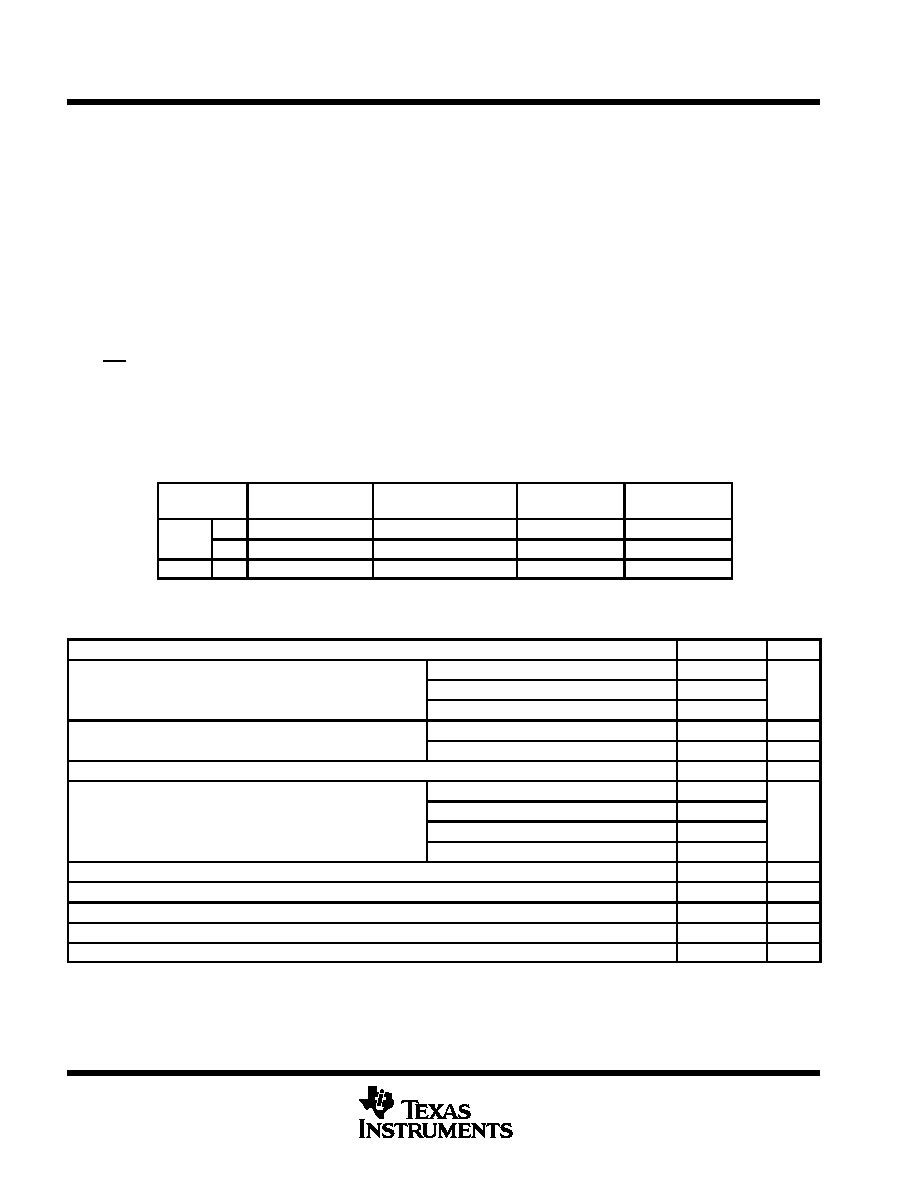
AVAILABLE OPTIONS
PACKAGED DEVICES
TA
PLASTIC SMALL OUTLINE
PowerPAD
PLASTIC
SMALL OUTLINE
DB-24
DB-30
SMALL OUTLINE
(PWP-24)
40
∞
C to
TPS2223DB, TPS2224DB
TPS2226DB
TPS2223PWP
≠ 40
∞
C to
85
∞
C
Pin compatibles
TPS2214, TPS2214A
Pin compatibles
TPS2216, TPS2216A,
TPS2206
TPS2223PWP,
TPS2224PWP
The DB and PWP packages are also available taped and reeled. Add R suffix to device type (e.g., TPS2223PWPR) for taped and reeled.
Copyright
2001, Texas Instruments Incorporated
PRODUCTION DATA information is current as of publication date.
Products conform to specifications per the terms of Texas Instruments
standard warranty. Production processing does not necessarily include
testing of all parameters.
Please be aware that an important notice concerning availability, standard warranty, and use in critical applications of
Texas Instruments semiconductor products and disclaimers thereto appears at the end of this data sheet.
PowerPAD is a trademark of Texas Instruments.
CardBus and PC Card are trademarks of PCMCIA (Personal Computer Memory Card International Association).
24
23
22
21
20
19
18
17
16
15
14
13
1
2
3
4
5
6
7
8
9
10
11
12
TPS2223, TPS2224
DB OR PWP PACKAGE
(TOP VIEW)
5V
5V
DATA
CLOCK
LATCH
NC
12V
AVPP
AVCC
AVCC
GND
RESET
5V
NC
NC
SHDN
12V
BVPP
BVCC
BVCC
NC
OC
3.3V
3.3V
NC ≠ No internal connection
Pin 7 and 20 are NC for TPS2223.
TPS2223, TPS2224, TPS2226
DUAL-SLOT CARDBUS POWER-INTERFACE SWITCHES
FOR SERIAL PCMCIA CONTROLLERS
SLVS317 ≠ MAY 2001
2
POST OFFICE BOX 655303
∑
DALLAS, TEXAS 75265
1
2
3
4
5
6
7
8
9
10
11
12
13
14
15
30
29
28
27
26
25
24
23
22
21
20
19
18
17
16
5V
5V
DATA
CLOCK
LATCH
NC
12V
AVPP
AVCC
AVCC
AVCC
GND
NC
RESET
3.3V
5V
NC
NC
NC
NC
SHDN
12V
BVPP
BVCC
BVCC
BVCC
NC
OC
3.3V
3.3V
TPS2226
DB PACKAGE
(TOP VIEW)
NC ≠ No internal connection
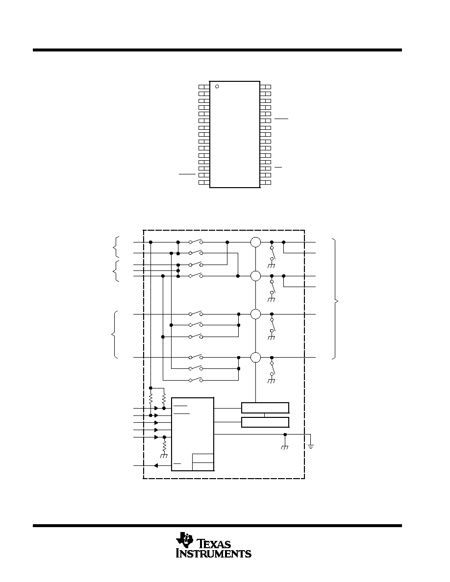
functional block diagram
CS
CS
S1
S4
CS
S7
CS
S11
Control Logic
SHDN
RESET
DATA
CLOCK
LATCH
OC
GND
UVLO
POR
Current Limit
Thermal Limit
S2
S5
S3
S6
S8
S9
S10
S12
S13
S14
Discharge
Element
13
14
3.3 V
3.3 V
Power
Inputs
3.3V
1
2
24
5 V
5 V
5 V
Power
Inputs
5V
7
12 V
ß
Power
Inputs
12V
∂
20
12 V
ß
21
12
3
4
5
15
9
10
AVCC
AVCC
17
18
BVCC
BVCC
8
AVPP
19
BVPP
11
Power Outputs
ß
Diagram shown for 24-pin DB package.
Current sense
ß The two 12-V pins must be externally connected.
∂ No Connections for TPS2223

TPS2223, TPS2224, TPS2226
DUAL-SLOT CARDBUS POWER-INTERFACE SWITCHES
FOR SERIAL PCMCIA CONTROLLERS
SLVS317 ≠ MAY 2001
3
POST OFFICE BOX 655303
∑
DALLAS, TEXAS 75265
Terminal Functions
TERMINAL
NAME
NO.
I/O
DESCRIPTION
NAME
TPS2223
TPS2224
TPS2226
3.3V
13, 14
13, 14
15, 16, 17
I
3.3-V input for card power and chip power
5V
1, 2, 24
1, 2, 24
1, 2, 30
I
5-V input for card power
12V
NA
7, 20
7, 24
I
12-V input for card power (xVPP). The two 12-V pins must be externally connected.
AVCC
9, 10
9, 10
9, 10, 11
O
Switched output that delivers 3.3 V, 5 V, ground or high impedance to card
AVPP
8
8
8
O
Switched output that delivers 3.3 V, 5 V, 12 V, ground or high impedance to card
(12 V not applicable to TPS2223)
BVCC
17, 18
17, 18
20, 21, 22
O
Switched output that delivers 3.3 V, 5 V, ground or high impedance to card
BVPP
19
19
23
O
Switched output that delivers 3.3 V, 5 V, 12 V, ground or high impedance to card
(12 V not applicable for TPS2223)
GND
11
11
12
Ground
OC
15
15
18
O
Open-drain overcurrent reporting output that goes low when an overcurrent
condition exists. An external pullup is required.
SHDN
21
21
25
I
Hi-Z (open) all switches. Identical function to serial D8. Asynchronous active-low
command, internal pullup
RESET
12
12
14
I
Logic-level RESET input active low. Asynchronous active-low command, internal
pullup
CLOCK
4
4
4
I
Logic-level clock for serial data word
DATA
3
3
3
I
Logic-level serial data word
LATCH
5
5
5
I
Logic-level latch for serial data word, internal pulldown
NC
6, 7, 16,
20, 22, 23
6, 16,
22, 23
6, 13, 19,
26 ≠ 29
No internal connection
TPS2223, TPS2224, TPS2226
DUAL-SLOT CARDBUS POWER-INTERFACE SWITCHES
FOR SERIAL PCMCIA CONTROLLERS
SLVS317 ≠ MAY 2001
4
POST OFFICE BOX 655303
∑
DALLAS, TEXAS 75265
absolute maximum ratings over operating free-air temperature (unless otherwise noted)
Input voltage range for card power: V
I(3.3V
)
≠ 0.3 V to 5.5 V
. . . . . . . . . . . . . . . . . . . . . . . . . . . . . . . . . . . . . . . . .
V
I(5V)
≠ 0.3 V to 5.5 V
. . . . . . . . . . . . . . . . . . . . . . . . . . . . . . . . . . . . . . . . . . .
V
I(12V)
≠ 0.3 V to 14 V
. . . . . . . . . . . . . . . . . . . . . . . . . . . . . . . . . . . . . . . . .
Logic input/output voltage
≠ 0.3 V to 6 V
. . . . . . . . . . . . . . . . . . . . . . . . . . . . . . . . . . . . . . . . . . . . . . . . . . . . . . . . . . .
Output voltage: V
O(xVCC)
≠ 0.3 V to 6 V
. . . . . . . . . . . . . . . . . . . . . . . . . . . . . . . . . . . . . . . . . . . . . . . . . . . . . . . . . . .
V
O(xVPP)
≠ 0.3 V to 14 V
. . . . . . . . . . . . . . . . . . . . . . . . . . . . . . . . . . . . . . . . . . . . . . . . . . . . . . . . . .
Continuous total power dissipation
See Dissipation Rating Table
. . . . . . . . . . . . . . . . . . . . . . . . . . . . . . . . . . . . .
Output current: I
O(xVCC)
Internally
Limited
. . . . . . . . . . . . . . . . . . . . . . . . . . . . . . . . . . . . . . . . . . . . . . . . . . . . . . . .
I
O(xVPP)
Internally
Limited
. . . . . . . . . . . . . . . . . . . . . . . . . . . . . . . . . . . . . . . . . . . . . . . . . . . . . . . . .
Operating virtual junction temperature range, T
J
≠ 40
∞
C to 100
∞
C
. . . . . . . . . . . . . . . . . . . . . . . . . . . . . . . . . . . . .
Storage temperature range, T
STG
≠ 55
∞
C to 150
∞
C
. . . . . . . . . . . . . . . . . . . . . . . . . . . . . . . . . . . . . . . . . . . . . . . . . .
Lead temperature 1.6 mm (1/16 inch) from case for 10 seconds)
260
∞
C
. . . . . . . . . . . . . . . . . . . . . . . . . . . . . . .
OC sink current
10 mA
. . . . . . . . . . . . . . . . . . . . . . . . . . . . . . . . . . . . . . . . . . . . . . . . . . . . . . . . . . . . . . . . . . . . . . . . . .
Stresses beyond those listed under "absolute maximum ratings" may cause permanent damage to the device. These are stress ratings only, and
functional operation of the device at these or any other conditions beyond those indicated under "recommended operating conditions" is not
implied. Exposure to absolute-maximum-rated conditions for extended periods may affect device reliability.
Not applicable for TPS2223
DISSIPATION RATING TABLE
PACKAGEß
TA
25
∞
C
POWER RATING
DERATING FACTOR
ABOVE TA = 25
∞
C
TA = 70
∞
C
POWER RATING
TA = 85
∞
C
POWER RATING
DB
24
890 mW
8.9 mW/
∞
C
489 mW
356 mW
DB
30
1095 mW
10.95 mW/
∞
C
602 mW
438 mW
PWP
24
3322 mW
33.22 mW/
∞
C
1827 mW
1329 mW
ß These devices are mounted on an JEDEC low-k board (2-oz. traces on surface).
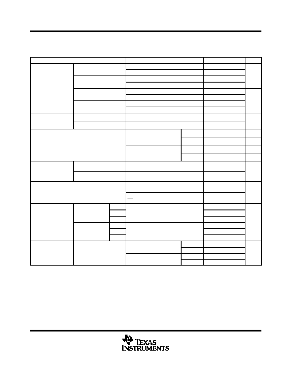
recommended operating conditions
MIN
MAX
UNIT
I
t
lt
V
i
i d f
ll i
it
ti
5V
d
VI(3.3V)∂
3
3.6
Input voltage, VI(3.3V) is required for all circuit operations. 5V and
12V are only required for their respective functions
VI(5V)
3
5.5
V
12V are only required for their res ective functions.
VI(12V)
7
13.5
Output current IO
IO(xVCC) at TJ = 100
∞
C
1
A
Output current, IO
IO(xVPP) at TJ = 100
∞
C
100
mA
Clock frequency, f(clock)
2.5
MHz
Data
200
Pulse duration t
Latch
250
ns
Pulse duration, tw
Clock
100
ns
Reset
100
Data-to-clock hold time (see Figure 2)
100
ns
Data-to-clock setup time, tsu (see Figure 2)
100
ns
Latch delay time, td(latch) (see Figure 2)
100
ns
Clock delay time, td(clock) (see Figure 2)
250
ns
Operating virtual junction temperature, TJ (maximum to be calculated at worst cast PD at 85
∞
C ambient)
≠ 40
100
∞
C
Not applicable for TPS2223
∂ It is understood that for VI(3.3V)< 3 V, voltages within the absolute maximum ratings applied to pin 5V or pin 12V will not damage the IC.
TPS2223, TPS2224, TPS2226
DUAL-SLOT CARDBUS POWER-INTERFACE SWITCHES
FOR SERIAL PCMCIA CONTROLLERS
SLVS317 ≠ MAY 2001
5
POST OFFICE BOX 655303
∑
DALLAS, TEXAS 75265
electrical characteristics, T
J
= 25
∞
C, V
I(5V)
= 5 V, V
I(3.3V)
= 3.3 V, V
I(12V)
= 12 V (not applicable for
TPS2223), all outputs unloaded (unless otherwise noted)
power switch
PARAMETER
TEST CONDITIONS
MIN
TYP
MAX
UNIT
3.3V to xVCC , with two
IO = 750 mA each
85
110
,
switches on
IO = 750 mA each, TJ = 100
∞
C
110
140
m
Static
5V to xVCC , with two
IO = 500 mA each
95
130
m
rDS( )
Static
drain-source
,
switches on
IO = 500 mA each, TJ = 100
∞
C
120
160
rDS(on)
on-state
i t
3.3V or 5V to xVPP , with two
IO = 50 mA each
0.8
1
resistance
,
switches on
IO = 50 mA each, TJ = 100
∞
C
1
1.3
12V to xVPP , with two
IO = 50 mA each
2
2.5
,
switches on
IO = 50 mA each, TJ = 100
∞
C
2.5
3.4
Output
discharge
Discharge at xVCC
IO(disc) = 1 mA
0.5
0.7
1
k
discharge
resistance
Discharge at xVPP
IO(disc) = 1 mA
0.2
0.4
0.5
k
Limit (steady-state value),
output powered into a short
IOS(xVCC)
1
1.4
2
A
IOS
Short circuit output current
output powered into a short
circuit
IOS(xVPP)
120
200
300
mA
IOS
Short-circuit output current
Limit (steady-state value),
output powered into a short
IOS(xVCC)
1
1.4
2
A
output powered into a short
circuit, TJ = 100
∞
C
IOS(xVPP)
120
200
300
mA
Thermal
shutdown
Thermal trip point, TJ
Rising temperature
135
∞
C
temperature
(see Note 1)
Hysteresis, TJ
10
∞
C
Current limit response time (see Note 1)
VO(xVCC) with 100-m
short, from short to
OC signal falling edge
10
µ
s
Current-limit response time (see Note 1)
VO(xVPP) with 100-m
short, from short to
OC signal falling edge
3
µ
s
N
l
ti
II(3.3V)
140
200
Normal operation
and reset mode
II(5V)
8
12
II
Input
current
and reset mode
II(12V)
100
180
µ
A
II
current,
quiescent
Shutdown mode,
II(3.3V)
0.3
2
µ
A
quiescent
Shutdown mode,
VO(xVCC) = Hi-Z,
II(5V)
0.1
2
(
)
VO(xVPP) = Hi-Z
II(12V)
0.3
2
Leakage
VO(xVCC) = 5 V,
10
Ilk
Leakage
current,
Shutdown mode
O(xVCC)
,
VI(5V) = VI(12V) = 0
TJ = 100
∞
C
50
µ
A
Ilkg
,
output off
t t
Shutdown mode
VO(xVPP) = 12 V,
10
µ
A
state
O(xVPP)
,
VI(5V) = VI(12V) = 0
TJ = 100
∞
C
50
Pulse-testing techniques maintain junction temperature close to ambient temperature; thermal effects must be taken into account separately.
NOTE 1: Specified by design; not tested in production.