TPS2392
TPS2393
SLUS536C - AUGUST 2002 - REVISED AUGUST 2004
FULL FEATURED -48 V
HOT SWAP POWER MANAGER
FEATURES
D
Wide Input Supply Range: -20 V to -80 V
D
Transient Rating to -100 V
D
Programmable Current Limit
D
Programmable Current Slew Rate
D
Programmable UV/OV Thresholds/Hysteresis
D
Debounced Insertion Detection Inputs
D
Open-Drain Power Good (PG) Output
D
Fault Timer to Eliminate Nuisance Trips
D
Open-Drain Fault Output (FAULT)
D
Enable Input (EN)
D
14-Pin TSSOP package
D
44-Pin TSSOP Package for
Creapage/Clearance
APPLICATIONS
D
-48-V Distributed Power Systems
D
Central Office Switching
D
Wireless Base Station
DESCRIPTION
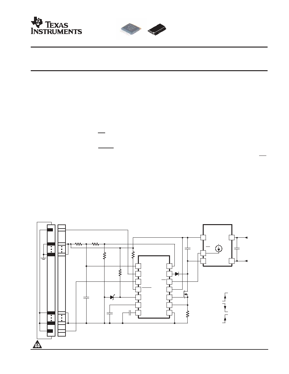
The TPS2392 and TPS2393 integrated circuits are hot
swap power managers optimized for use in nominal
-48-V systems. They operate with supply voltage
ranges from -20-V to -80-V, and are rated to withstand
spikes to -100 V. In conjunction with an external
N-channel FET and sense resistor, they can be used to
enable live insertion of plug-in cards and modules in
powered systems. Each device provides load current
slew rate control and peak magnitude limiting.
Undervoltage and overvoltage shutdown thresholds
are easily programmed via a three-resistor divider
network. In addition, two active-low, debounced inputs
provide plug-in insertion detection. A power good (PG)
output enables downstream converters. The TPS2392
and TPS2393 also provide the basic hot swap functions
of electrical isolation of faulty cards, filtered protection
against nuisance overcurrent trips, and single-line fault
reporting. The 44-pin part supports designs where
telecomm creepage and clearance requirements must
be followed.
The TPS2392 latches off in response to current faults,
while the TPS2393 periodically retries the load in the
event of a fault.
UDG-02098
D1
BAS19
C2
0.1
�
F
R3
3.92 k
1%
R2
4.99 k
1%
R1
200 k
1%
R4
20 m
1/4, 1%
R6
10 k
R5
100
k
C4
100
�
F
100 V
COUT
= 32.8 V
= 30.8 V
= 72.6 V
VUV
VUV
VOV
GATE
1
2
3
4
5
6
7
14
13
12
11
10
9
8
UVLO
INSA
INSB
FAULT
EN
FLTTIME
OVLO
DRAINSNS
ISENS
IRAMP
-VIN
PG
RTN
TPS2392/TPS2393
VOUT+
VOUT-
VIN+
VIN-
DC/DC
CONVERTER
EN
VDD
C3
1500 pF
VOUT+
VOUT-
GND
C1
3900 pF
-48V
Q1
IRF530
D2
5.6 V
PRODUCTION DATA information is current as of publication date. Products
conform to specifications per the terms of Texas Instruments standard warranty.
Production processing does not necessarily include testing of all parameters.
.
Please be aware that an important notice concerning availability, standard warranty, and use in critical applications of Texas Instruments
semiconductor products and disclaimers thereto appears at the end of this data sheet.
www.ti.com
Copyright
2004, Texas Instruments Incorporated
TPS2392
TPS2393
SLUS536C - AUGUST 2002 - REVISED AUGUST 2004
www.ti.com
2
These devices have limited built-in ESD protection. The leads should be shorted together or the device placed in conductive foam during
storage or handling to prevent electrostatic damage to the MOS gates.
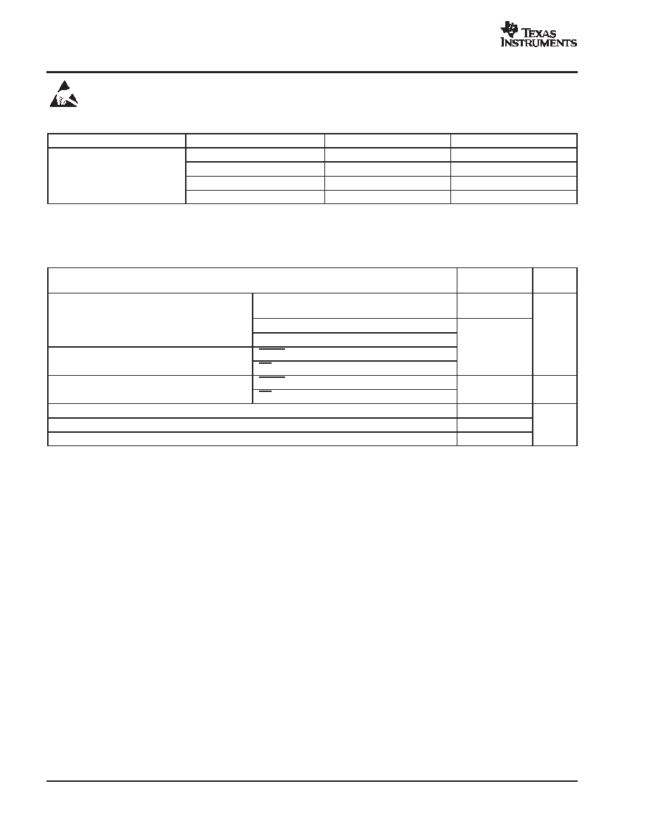
ORDERING INFORMATION
TA
FAULT OPERATION
PACKAGE
PART NUMBER
LATCH OFF
TSSOP (PW)(1)
TPS2392PW
-40
�
C to 85
�
C
PERIODIC RETRY
TSSOP (PW)(1)
TPS2393PW
-40
�
C to 85
�
C
LATCH OFF
TSSOP (PW)(1)
TPS2392DBT
PERIODIC RETRY
TSSOP (PW)(1)
TPS2393DBT
(1) The PW and DBT package is also available taped and reeled. Add an R suffix to the device type (i.e., TPS2392PWR) for quantities of 2,500 per
reel.
ABSOLUTE MAXIMUM RATINGS
over operating free-air temperature range unless otherwise noted(1)
TPS2392
TPS2393
UNIT
Input voltage range, VI
UVLO, INSA, INSB, FLTTIME, IRAMP, OVLO,
DRAINSNS, GATE, ISENS(2)
-0.3 to 15
Input voltage range, VI
RTN(2)
V
EN(2)(3)
-0.3 to 100
V
Output voltage range, VO
FAULT(2)(4)
-0.3 to 100
Output voltage range, VO
PG(2)(4)
Continuous output current
FAULT
10
mA
Continuous output current
PG
10
mA
Operating junction temperature range, TJ
-55 to 125
Storage temperature, Tstg
-65 to 150
�
C
Lead temperature 1,6 mm (1/16 inch) from case for 10 seconds
260
C
(1) Stresses beyond those listed under "absolute maximum ratings" may cause permanent damage to the device. These are stress ratings only, and
functional operation of the device at these or any other conditions beyond those indicated under "recommended operating conditions" is not
implied. Exposure to absolute-maximum-rated conditions for extended periods may affect device reliability.
(2) All voltages are with respect to -VIN (unless otherwise noted).
(3) With 100-k
minimum input series resistance.
(4) With 10-k
minimum series resistance.

TPS2392
TPS2393
SLUS536C - AUGUST 2002 - REVISED AUGUST 2004
www.ti.com
3
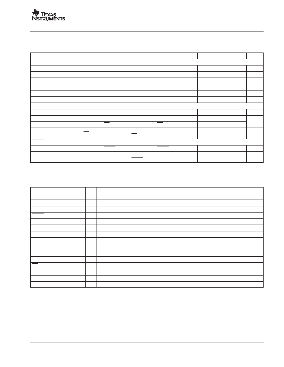
RECOMMENDED OPERATING CONDITIONS
MIN
NOM
MAX
UNIT
Input supply voltage, -VIN to RTN
-80
-20
V
Operating junction temperature, TJ
-40
85
�
C
DISSIPATION RATINGS
PACKAGE
TA < 25
�
C
POWER RATING
DERATING FACTOR
ABOVE TA = 25
�
C
TA = 85
�
C
POWER RATING
TSSOP-14
750 mW
7.5 mW/
�
C
300 mW
1
2
3
4
5
6
7
14
13
12
11
10
9
8
UVLO
INSA
INSB
FAULT
EN
FLTTIME
IRAMP
OVLO
DRAINSNS
PG
RTN
GATE
ISENS
-VIN
PW PACKAGE
(TOP VIEW)
1
2
3
4
5
6
7
8
9
10
11
12
13
14
15
16
17
18
19
20
21
22
44
43
42
41
40
39
38
37
36
35
34
33
32
31
30
29
28
27
26
25
24
23
INSA
N/C
N/C
N/C
N/C
N/C
INSB
N/C
N/C
N/C
N/C
N/C
FAULT(BAR)
EN
FLTTIME
IRAMP
N/C
N/C
N/C
N/C
N/C
-VIN
UVLO
OVLO
N/C
DRAIN SENSE
PG(BAR)
N/C
N/C
N/C
N/C
N/C
RTN
N/C
N/C
N/C
N/C
N/C
GATE
ISENS
N/C
N/C
N/C
N/C
DBT PACKAGE
(TOP VIEW)

TPS2392
TPS2393
SLUS536C - AUGUST 2002 - REVISED AUGUST 2004
www.ti.com
4
ELECTRICAL CHARACTERISTICS
VI(-VIN) = -48 V with respect to RTN, VI(EN) = 2.8 V, VI(INSA) = 0 V, VI(INSB) = 0 V, VI(UVLO) = 2.5 V, VI(OVLO) = 0 V, VI(ISENS) = 0 V, all outputs
unloaded, TA = -40
�
C to 85
�
C (unless otherwise noted)(1)(2)
PARAMETER
TEST CONDITIONS
MIN
TYP
MAX
UNIT
INPUT SUPPLY
ICC1
Supply current, RTN
VI(RTN) = 48 V
1050
1500
A
ICC2
Supply current, RTN
VI(RTN) = 80 V
1350
1700
�
A
VUVLO_L Internal UVLO threshold, VIN rising
To GATE pull-up
-19
-16
-13
V
VHYS
Internal UVLO hysteresis
200
mV
ENABLE INPUT (EN)
VTH
Threshold voltage, VIN rising
To GATE pull-up
1.3
1.4
1.5
V
ISRC_EN EN pin switched pull-up current
-12
-10
-8
�
A
UNDERVOLTAGE/OVERVOLTAGE COMPARATORS
VTH_UV
Threshold voltage, VIN rising, UVLO
To GATE pull-up
1.36
1.40
1.44
V
ISRC_UV UVLO pin switched pull-up current
VI(UVLO) = 2.5 V
-11.7
-10.0
-8.3
�
A
IIL
UVLO low-level input current
VI(UVLO) = 1 V
-1
1
�
A
VTH_OV
Threshold voltage, VIN rising, OVLO
To GATE pull-up
1.36
1.40
1.44
V
ISRC_OV OLVO pin switched pull-up current
VI(OVLO) = 2.5 V
-11.7
-10.0
-8.3
�
A
IIL
OVLO low-level input current
VI(OVLO) = 1 V
-1
1
�
A
INSERTION DETECTION
VTH
Threshold voltage, VIN rising, INSA, INSB
To GATE pull-down
1.0
1.4
1.8
V
ISRC_INSx INSA, INSB pin pull-up current
VI(INSA) = 0 V, VI(INSB) = 0 V
-14
-11
-8
�
A
tD_INS
Insertion delay time, VIN falling, INSA, INSB
To GATE pull-up
1.5
2.5
4.1
ms
LINEAR CURRENT AMPLIFIER (LCA)
VOH
High-level output voltage, GATE
VI(ISENS) = 0 V, IO(GATE) = -10
�
A
11
14
17
V
ISINK
Output sink current, linear mode
VI(ISENS) = 80 mV, VO(GATE) = 5 V
VO(FLTTIME) = 2 V
5
10
mA
IFAULT
Output sink current, fault shutdown
VI(ISENS) = 80 mV, VO(GATE) = 5 V
VO(FLTTIME) > 4 V
50
100
mA
II
Input current, ISENS
0 V < VI(ISENS) < 0.2 V
-1
1
�
A
VREF_K
Reference clamp voltage
VO(IRAMP) = OPEN
33
40
47
mV
VIO
Input offset voltage
VO(IRAMP) = 2 V
-7
7
mV
RAMP GENERATOR
ISRC1
IRAMP source current, reduced rate turn-on
VO(IRAMP) = 0.25 V
-850
-600
-400
nA
ISRC2
IRAMP source current, normal rate
VO(IRAMP) = 1 V
-11
-10
-9
A
ISRC2
IRAMP source current, normal rate
VO(IRAMP) = 3 V
-11
-10
-9
�
A
VOL
Low-level output voltage, IRAMP
VI(EN) = 0 V
2
mV
AV
Voltage gain, relative to ISENS
9.5
10.0
10.5
mV/V
OVERLOAD COMPARATOR
VTH_OL
Current overload threshold, ISENS
80
100
120
mV
tDLY
Glitch filter delay time
VI(ISENS) = 200 mV
2
4
7
�
s
(1)
All voltages are with respect to the -VIN terminal, unless otherwise stated.
(2)
Currents are positive into and negative out of the specified terminals.
TPS2392
TPS2393
SLUS536C - AUGUST 2002 - REVISED AUGUST 2004
www.ti.com
5
ELECTRICAL CHARACTERISTICS (continued)
VI(-VIN) = -48 V with respect to RTN, VI(EN) = 2.8 V, VI(INSA) = 0 V, VI(INSB) = 0 V, VI(UVLO) = 2.5 V, VI(OVLO) = 0 V, VI(ISENS) = 0 V, all outputs
unloaded, TA = -40
�
C to 85
�
C (unless otherwise noted)
PARAMETER
TEST CONDITIONS
MIN
TYP
MAX
UNIT
FAULT TIMER
VOL
Low-level output voltage, FLTTIME
VI(EN) = 0 V
5
mV
ICHG
Charging current, current limit mode
VI(ISENS) = 80 mV, VO(FLTTIME) = 2 V
-55
-50
-45
�
A
VFLT
Fault threshold voltage
3.75
4.00
4.25
V
IDSG
Discharge current, retry mode TPS2393
VI(ISENS) = 80 mV, VO(FLTTIME) = 2 V
0.38
0.61
�
A
D
Output duty cycle TPS2393
VI(ISENS) = 80 mV
1.0%
1.5%
IRST
Discharge current, timer reset mode
VO(FLTTIME) = 2 V, VI(ISENS) = 0 V
1
mA
POWERGOOD SENSING
VTH
DRAINSNS threshold voltage
1.20
1.35
1.50
V
ISRC
DRAINSNS pull-up current
VI(DRAINSNS) = 0 V
-14
-11
-8
A
IOH
High-level output leakage current, PG output
VI(EN) = 0 V, VO(PG) = 65 V
10
�
A
RDS(on) Driver on-resistance, PG output
VI(ISENS) = 0 V, VI(DRAINSNS) = 0 V
IO(PG) = 1 mA
50
80
FAULT OUTPUT
IOH
High-level output leakage current, FAULT
VI(EN) = 0 V, VO(FAULT) = 65 V
10
�
A
RDS(on) Driver on-resistance, FAULT
VI(ISENS) = 80 V, VO(FLTTIME) = 5 V
IO(FAULT) = 1 mA
50
80
(1)
All voltages are with respect to the -VIN terminal, unless otherwise stated.
(2)
Currents are positive into and negative out of the specified terminals.
TERMINAL FUNCTIONS
TERMINAL
I/O
DESCRIPTION
NAME
PW
DBT
I/O
DESCRIPTION
DRAINSNS
13
41
I
Sense input for monitoring the load voltage status
EN
5
14
I
Enable input to turn on/off power to the load
FAULT
4
13
O
Open-drain, active-low indication of a load fault condition
FLTTIME
6
15
I/O
Connection for user-programming of the fault timeout period
GATE
10
28
O
Gate drive for external N-channel FET
INSA
2
1
I
Insertion detection input pin A
INSB
3
7
I
Insertion detection input pin B
IRAMP
7
16
I/O
Programming input for setting the inrush current slew rate
ISENS
9
27
I
Current sense input
OVLO
14
43
I
Voltage sense input for supply overvoltage lockout (OVLO) protection
PG
12
40
O
Open-drain, active-low indication of load power-good condition
RTN
11
34
I
Positive supply input
UVLO
1
44
I
Voltage sense input for supply undervoltage lockout (UVLO) protection
-VIN
8
22
I
Negative supply input and reference pin