 | –≠–ª–µ–∫—Ç—Ä–æ–Ω–Ω—ã–π –∫–æ–º–ø–æ–Ω–µ–Ω—Ç: TPS2837 | –°–∫–∞—á–∞—Ç—å:  PDF PDF  ZIP ZIP |

TPS2836, TPS2837
SYNCHRONOUS-BUCK MOSFET DRIVER
WITH DEADTIME CONTROL
SLVS224 ≠ NOVEMBER 1999
1
POST OFFICE BOX 655303
∑
DALLAS, TEXAS 75265
D
Floating Bootstrap or Ground-Reference
High-Side Driver
D
Active Deadtime Control
D
50-ns Max Rise/Fall Times With
3.3-nF Load
D
2-A Min Peak Output Current
D
4.5-V to 15-V Supply Voltage Range
D
TTL-Compatible Inputs
D
Internal Schottky Bootstrap Diode
D
Low Supply Current . . . 3 mA Typ
D
Ideal for High-Current Single- or Multiphase
Applications
D
≠40
∞
C to 125
∞
C Junction-Temperature
Operating Range
description
The TPS2836 and TPS2837 are MOSFET drivers for synchronous-buck power stages. These devices are ideal
for designing a high-performance power supply using a switching controller that does not include suitable
on-chip MOSFET drivers. The drivers are designed to deliver minimum 2-A peak currents into large capacitive
loads. The high-side driver can be configured as ground-reference or as floating-bootstrap. An adaptive
dead-time control circuit eliminates shoot-through currents through the main power FETs during switching
transitions and provides high efficiency for the buck regulator.
The TPS2836 has a noninverting input, while the TPS2837 has an inverting input. These drivers, available in
8-terminal SOIC packages, operate over a junction temperature range of ≠40
∞
C to 125
∞
C.
AVAILABLE OPTIONS
PACKAGED DEVICES
TJ
SOIC
(D)
≠40
∞
C to 125
∞
C
TPS2836D
TPS2837D
The D package is available taped and reeled. Add R
suffix to device type (e.g., TPS2836DR)
Copyright
©
1999, Texas Instruments Incorporated
PRODUCTION DATA information is current as of publication date.
Products conform to specifications per the terms of Texas Instruments
standard warranty. Production processing does not necessarily include
testing of all parameters.
Please be aware that an important notice concerning availability, standard warranty, and use in critical applications of
Texas Instruments semiconductor products and disclaimers thereto appears at the end of this data sheet.
D PACKAGE
(TOP VIEW)
1
2
3
4
8
7
6
5
IN
PGND
DT
V
CC
BOOT
HIGHDR
BOOTLO
LOWDR
TPS2836, TPS2837
SYNCHRONOUS-BUCK MOSFET DRIVER
WITH DEADTIME CONTROL
SLVS224 ≠ NOVEMBER 1999
2
POST OFFICE BOX 655303
∑
DALLAS, TEXAS 75265
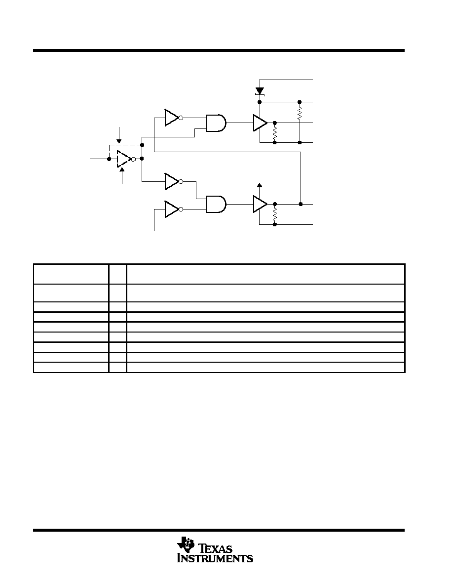
functional block diagram
DT
3
IN
VCC
LOWDR
BOOTLO
HIGHDR
BOOT
PGND
1
4
8
7
6
5
VCC
2
(TPS2836 Only)
(TPS2837 Only)
200 k
200 k
200 k
Terminal Functions
TERMINAL
I/O
DESCRIPTION
NAME
NO.
I/O
DESCRIPTION
BOOT
8
I
Bootstrap terminal. A ceramic capacitor is connected between BOOT and BOOTLO to develop the floating
bootstrap voltage for the high-side MOSFET. The capacitor value is typically between 0.1
µ
F and 1
µ
F.
BOOTLO
6
O
This terminal connects to the junction of the high-side and low-side MOSFETs.
DT
3
I
Deadtime control terminal. Connect DT to the junction of the high-side and low-side MOSFETs
HIGHDR
7
O
Output drive for the high-side power MOSFET
IN
1
I
Input signal to the MOSFET drivers (noninverting input for the TPS2836; inverting input for the TPS2837).
LOWDR
5
O
Output drive for the low-side power MOSFET
PGND
2
Power ground. Connect to the FET power ground.
VCC
4
I
Input supply. Recommended that a 1
µ
F capacitor be connected from VCC to PGND.

TPS2836, TPS2837
SYNCHRONOUS-BUCK MOSFET DRIVER
WITH DEADTIME CONTROL
SLVS224 ≠ NOVEMBER 1999
3
POST OFFICE BOX 655303
∑
DALLAS, TEXAS 75265
detailed description
low-side driver
The low-side driver is designed to drive low r
DS(on)
N-channel MOSFETs. The current rating of the driver is 2 A,
source and sink.
high-side driver
The high-side driver is designed to drive low r
DS(on)
N-channel MOSFETs. The current rating of the driver is 2 A,
source and sink. The high-side driver can be configured as a ground-reference driver or a floating bootstrap
driver. The internal bootstrap diode, is a Schottky for improved drive efficiency. The maximum voltage that can
be applied between the BOOT terminal and ground is 30 V.
dead-time (DT) control
Dead-time control prevents shoot-through current from flowing through the main power FETs during switching
transitions by controlling the turnon times of the MOSFET drivers. The high-side driver is not allowed to turn
on until the gate drive voltage to the low-side FET is low, and the low-side driver is not allowed to turn on until
the voltage at the junction of the power FETs (Vdrn) is low; the TTL-compatible DT terminal connects to the
junction of the power FETs.
IN
The IN terminal is a TTL-compatible digital terminal that is the input control signal for the drivers. The TPS2836
has a noninverting input; the TPS2837 has an inverting input.
TPS2836, TPS2837
SYNCHRONOUS-BUCK MOSFET DRIVER
WITH DEADTIME CONTROL
SLVS224 ≠ NOVEMBER 1999
4
POST OFFICE BOX 655303
∑
DALLAS, TEXAS 75265
absolute maximum ratings over operating free-air temperature (unless otherwise noted)
Supply voltage range, V
CC
(see Note 1)
≠0.3 V to 16 V
. . . . . . . . . . . . . . . . . . . . . . . . . . . . . . . . . . . . . . . . . . . . .
Input voltage range: BOOT to PGND (high-side driver ON)
≠0.3 V to 30 V
. . . . . . . . . . . . . . . . . . . . . . . . . . . . .
BOOTLO to PGND
≠0.3 V to 16 V
. . . . . . . . . . . . . . . . . . . . . . . . . . . . . . . . . . . . . . . . . . . . . .
BOOT to BOOTLO
≠0.3 V to 16 V
. . . . . . . . . . . . . . . . . . . . . . . . . . . . . . . . . . . . . . . . . . . . . .
IN
≠0.3 V to 16 V
. . . . . . . . . . . . . . . . . . . . . . . . . . . . . . . . . . . . . . . . . . . . . . . . . . . . . . . . . . . . .
DT
≠0.3 V to 30 V
. . . . . . . . . . . . . . . . . . . . . . . . . . . . . . . . . . . . . . . . . . . . . . . . . . . . . . . . . . . .
Continuous total power dissipation
See Dissipation Rating Table
. . . . . . . . . . . . . . . . . . . . . . . . . . . . . . . . . . . . .
Operating virtual junction temperature range, T
J
≠40
∞
C to 125
∞
C
. . . . . . . . . . . . . . . . . . . . . . . . . . . . . . . . . . . . .
Storage temperature range, T
stg
≠ 65
∞
C to 150
∞
C
. . . . . . . . . . . . . . . . . . . . . . . . . . . . . . . . . . . . . . . . . . . . . . . . . . .
Lead temperature soldering 1,6 mm (1/16 inch) from case for 10 seconds
260
∞
C
. . . . . . . . . . . . . . . . . . . . . . .
Stresses beyond those listed under "absolute maximum ratings" may cause permanent damage to the device. These are stress ratings only, and
functional operation of the device at these or any other conditions beyond those indicated under "recommended operating conditions" is not
implied. Exposure to absolute-maximum-rated conditions for extended periods may affect device reliability.
NOTES:
1. Unless otherwise specified, all voltages are with respect to PGND.
DISSIPATION RATING TABLE
PACKAGE
TA
25
∞
C
POWER RATING
DERATING FACTOR
ABOVE TA = 25
∞
C
TA = 70
∞
C
POWER RATING
TA = 85
∞
C
POWER RATING
D
580 mW
5.8 mW/
∞
C
320 mW
232 mW
recommended operating conditions
MIN
NOM
MAX
UNIT
Supply voltage, VCC
4.5
15
V
Input voltage
BOOT to PGND
4.5
28
V
electrical characteristics over recommended operating virtual junction temperature range,
V
CC
= 6.5 V, C
L
= 3.3 nF (unless otherwise noted)
supply current
PARAMETER
TEST CONDITIONS
MIN
TYP
MAX
UNIT
VCC
Supply voltage range
4.5
15
V
VCC
Quiescent current
VCC =15 V,
V(ENABLE) = LOW
100
µ
A
VCC
Quiescent current
VCC =15 V,
V(ENABLE) = HIGH
300
400
µ
A
VCC
Quiescent current
VCC =12 V,
fSWX = 200 kHz,
CHIGHDR = 50 pF,
BOOTLO grounded,
CLOWDR = 50 pF,
See Note 2
3
mA
NOTE 2: Ensured by design, not production tested.
TPS2836, TPS2837
SYNCHRONOUS-BUCK MOSFET DRIVER
WITH DEADTIME CONTROL
SLVS224 ≠ NOVEMBER 1999
5
POST OFFICE BOX 655303
∑
DALLAS, TEXAS 75265
electrical characteristics over recommended operating virtual junction temperature range,
V
CC
= 6.5 V, C
L
= 3.3 nF (unless otherwise noted) (continued)
output drivers
PARAMETER
TEST CONDITIONS
MIN
TYP
MAX
UNIT
Hi h id
i k
Duty cycle < 2%,
VBOOT ≠ VBOOTLO = 4.5 V, VHIGHDR = 4 V
0.7
1.1
High-side sink
(see Note 4)
Duty cycle < 2%,
tpw < 100
µ
s
VBOOT ≠ VBOOTLO = 6.5 V, VHIGHDR = 5 V
1.1
1.5
A
(see Note 4)
(see Note 3)
VBOOT ≠ VBOOTLO = 12 V, VHIGHDR = 10.5 V
2
2.4
High-side
Duty cycle < 2%,
VBOOT ≠ VBOOTLO = 4.5 V, VHIGHDR = 0.5V
1.2
1.4
High side
source
Duty cycle < 2%,
tpw < 100
µ
s
VBOOT ≠ VBOOTLO = 6.5 V, VHIGHDR = 1.5 V
1.3
1.6
A
Peak output-
(see Note 4)
(see Note 3)
VBOOT ≠ VBOOTLO = 12 V, VHIGHDR = 1.5 V
2.3
2.7
current
L
id
i k
Duty cycle < 2%,
VCC = 4.5 V,
VLOWDR = 4 V
1.3
1.8
Low-side sink
(see Note 4)
Duty cycle < 2%,
tpw < 100
µ
s
VCC = 6.5 V,
VLOWDR = 5 V
2
2.5
A
(see Note 4)
(see Note 3)
VCC = 12 V,
VLOWDR = 10.5 V
3
3.5
Low-side
Duty cycle < 2%,
VCC = 4.5 V,
VLOWDR = 0.5V
1.4
1.7
Low side
source
Duty cycle < 2%,
tpw < 100
µ
s
VCC = 6.5 V,
VLOWDR = 1.5 V
2
2.4
A
(see Note 4)
(see Note 3)
VCC = 12 V,
VLOWDR = 1.5 V
2.5
3
VBOOT ≠ VBOOTLO = 4.5 V, VHIGHDR = 0.5 V
5
High-side sink (see Note 4)
VBOOT ≠ VBOOTLO = 6.5 V, VHIGHDR = 0.5 V
5
VBOOT ≠ VBOOTLO = 12 V, VHIGHDR = 0.5 V
5
VBOOT ≠ VBOOTLO = 4.5 V, VHIGHDR = 4 V
75
High-side source (see Note 4)
VBOOT ≠ VBOOTLO = 6.5 V, VHIGHDR = 6 V
75
Output
VBOOT ≠ VBOOTLO = 12 V, VHIGHDR =11.5 V
75
resistance
VDRV = 4.5 V,
VLOWDR = 0.5 V
9
Low-side sink (see Note 4)
VDRV = 6.5 V
VLOWDR = 0.5 V
7.5
VDRV = 12 V,
VLOWDR = 0.5 V
6
VDRV = 4.5 V,
VLOWDR = 4 V
75
Low-side source (see Note 4)
VDRV = 6.5 V,
VLOWDR = 6 V
75
VDRV = 12 V,
VLOWDR = 11.5 V
75
NOTES:
3. Ensured by design, not production tested.
4. The pullup/pulldown circuits of the drivers are bipolar and MOSFET transistors in parallel. The peak output current rating is the
combined current from the bipolar and MOSFET transistors. The output resistance is the rDS(on) of the MOSFET transistor when
the voltage on the driver output is less than the saturation voltage of the bipolar transistor.
deadtime
PARAMETER
TEST CONDITIONS
MIN
TYP
MAX
UNIT
LOWDR
High-level input voltage
Over the VCC range (see Note 3)
0.7VCC
V
LOWDR
Low-level input voltage
Over the VCC range (see Note 3)
1
V
DT
High-level input voltage
Over the VCC range
0.7VCC
V
DT
Low-level input voltage
Over the VCC range
1
V
NOTE 3: Ensured by design, not production tested.
digital control terminals (IN)
PARAMETER
TEST CONDITIONS
MIN
TYP
MAX
UNIT
High-level input voltage
Over the VCC range
2
V
Low-level input voltage
Over the VCC range
1
V