 | –≠–ª–µ–∫—Ç—Ä–æ–Ω–Ω—ã–π –∫–æ–º–ø–æ–Ω–µ–Ω—Ç: TPS61061 | –°–∫–∞—á–∞—Ç—å:  PDF PDF  ZIP ZIP |

www.ti.com
FEATURES
APPLICATIONS
DESCRIPTION
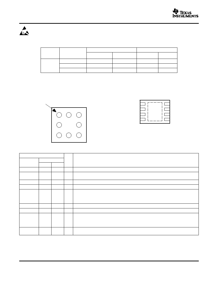
TYPICAL APPLICATION
VIN
EN
GND
SW
FB
OUT
ILED
PGND
VIN
2.7 V to 6 V
C1
1
m
F
L1
22
m
H
R
S
12
W
C2
220 nF
TPS61060
TPS61061
TPS61062
SLVS538 ≠ NOVEMBER 2004
CONSTANT CURRENT LED DRIVER WITH DIGITAL AND PWM BRIGHTNESS CONTROL
∑
Up to 80% Efficiency
∑
LED Driver With Integrated Overvoltage and
∑
8-Pin NanoFreeTMPackage (Chipscale, CSP)
Short-Circuit Protection
∑
3
◊
3-mm QFN Package
∑
2.7-V to 6.0-V Input Voltage Range
∑
500-mV/250-mV Feedback Voltage
∑
White LED Driver
∑
TPS61060 Powers Up to 3 LEDs
∑
Cellular Phones
∑
TPS61061 Powers Up to 4 LEDs
∑
PDA, Pocket PC, and Smart Phones
∑
TPS61062 Powers Up to 5 LEDs
∑
Digital Still Camera
∑
PWM Brightness Control on Enable
∑
Handheld Devices
∑
Digital Brightness Control on ILED
∑
1.0-MHz Fixed Switching Frequency
∑
400-mA Internal Power MOSFET Switch
∑
LEDs Disconnected During Shutdown
∑
Operates With Small-Output Capacitors
Down to 220 nF
The TPS61060/61/62 is a high-frequency, synchronous boost converter with constant current output to drive up
to 5 white LEDs. For maximum safety, the device features integrated overvoltage and an advanced short-circuit
protection when the output is shorted to ground. The device operates with 1-MHz fixed switching frequency to
allow small external components and to simplify possible EMI problems. The device comes with three different
overvoltage protection thresholds (14 V/18 V/23 V) to allow inexpensive and small-output capacitors with lower
voltage ratings. The LED current is initially set with the external sense resistor Rs, and the feedback voltage is
regulated to 500 mV or 250 mV, depending on the ILED pin configuration. Digital brightness control is
implemented by applying a simple digital signal to the ILED pin. Alternatively, a PWM signal up to 1 kHz can be
applied to the enable pin to control the LED brightness. During shutdown, the output is disconnected from the
input to avoid leakage current through the LEDs.
Figure 1.
Please be aware that an important notice concerning availability, standard warranty, and use in critical applications of Texas
Instruments semiconductor products and disclaimers thereto appears at the end of this data sheet.
NanoFree, PowerPAD are trademarks of Texas Instruments.
PRODUCTION DATA information is current as of publication date.
Copyright © 2004, Texas Instruments Incorporated
Products conform to specifications per the terms of the Texas
Instruments standard warranty. Production processing does not
necessarily include testing of all parameters.
www.ti.com
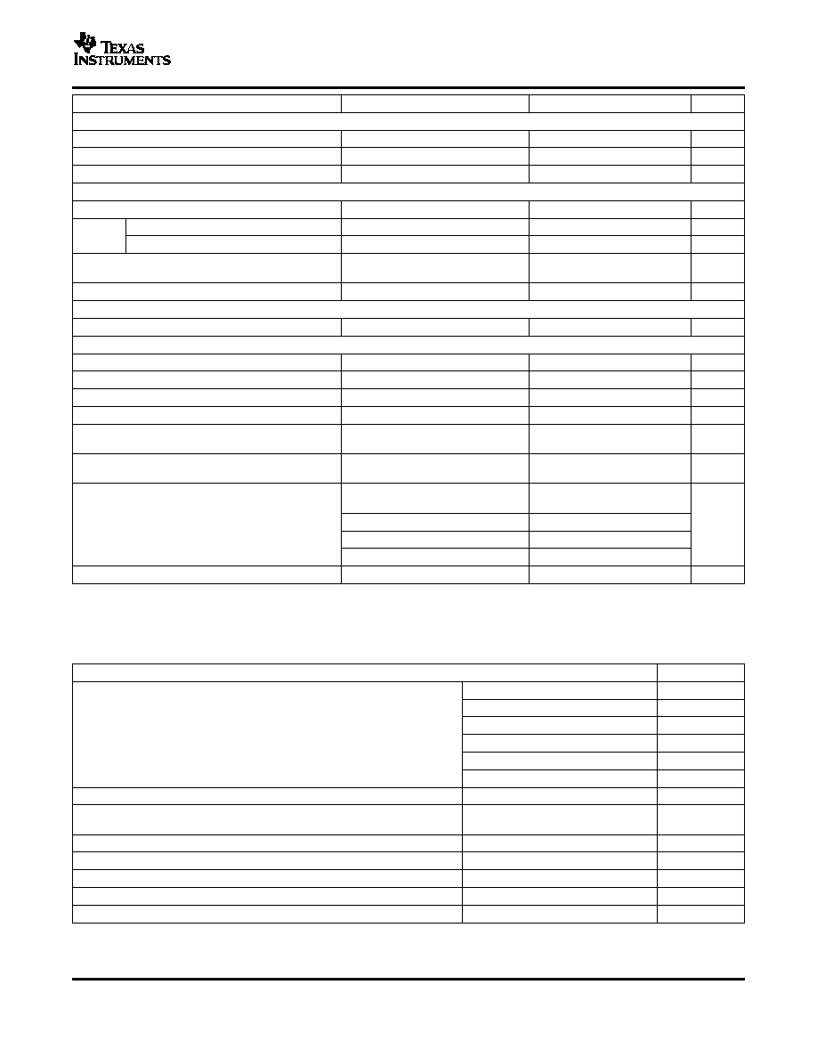
GND
EN
ILED
FB
Vin
OUT
SW
PGND
1
2
3
4
5
6
7
8
Exposed
Thermal
DiePad
A
B
C
1
2
3
Pin A1
Index
TPS61060
TPS61061
TPS61062
SLVS538 ≠ NOVEMBER 2004
These devices have limited built-in ESD protection. The leads should be shorted together or the device
placed in conductive foam during storage or handling to prevent electrostatic damage to the MOS gates.
ORDERING INFORMATION
OVERVOLTAGE
PACKAGE
PACKAGE MARKING
T
A
PROTECTION
NanoFree
QFN
NanoFree
(1)
QFN
(2)
(OVP)
14 V (min)
TPS61060YZF
TPS61060DRB
AKX
AQP
≠40 to 85
∞
C
18 V (min)
TPS61061YZF
TPS61061DRB
AKY
AQQ
22.2 V (min)
TPS61062YZF
TPS61062DRB
AKZ
AQR
(1)
The YZF package is available in tape and reel. Add R suffix (TPS61060YZFR) to order quantities of
3000 parts per reel or add T suffix (TPS61060YZFT) to order 250 parts per reel.
(2)
The DRB package is available in tape and reel. Add R suffix (TPS61060DRBR) to order quantities of
3000 parts per reel.
8-Pin NanoFree Package
8-Pin 3x3-mm QFN Package
Top View
Top View
TERMINAL FUNCTIONS
TERMINAL
NO.
I/O
DESCRIPTION
NAME
CSP
QFN
VIN
B1
8
I
Input supply pin of the device
Enable pin. This pin needs to be pulled high to enable the device. To allow brightness control of
EN
A2
2
I
the LEDs a PWM signal up to 1 kHz can be applied. This pin has an internal pulldown resistor.
GND
A1
1
Analog ground
PGND
C3
5
Power ground
This is the feedback pin of the device. The feedback pin regulates the LED current through the
sense resistor by regulating the voltage across Rs. The feedback voltage is set by the ILED pin.
FB
B3
4
I
ILED=GND sets the feedback voltage to 500 mV. ILED=high sets the feedback voltage to 250
mV. Refer to digital brightness control section for more information.
OUT
C1
7
O
Output of the device
SW
C2
6
I
Switch pin of the device
Digital brightness control input. When this pin is grounded the digital brightness control is
disabled. When this pin is connected to high then the feedback voltage is reduced to typically
ILED
A3
3
I
250 mV and the digital brightness control is enabled. Refer to digital brightness control section for
more information.
The PowerPADTM (exposed thermal diepad) is only available on the QFN package. The
PowerPADTM
≠
≠
PowerPADTM needs to be connected and soldered to analog ground (GND).
2

www.ti.com
Comparator
Error
Amplifier
FB
PGND
Q1
OUT
VIN
EN
Q2
EN
ILED
GND
EN
OVP
EN
EN
50-mS
Turnoff
Delay
Bias V
ref
= 1.22 V
Thermal Shutdown
UVLO
Pre-Charge Current/PWM
Short-Circuit Detection
SW
V
ref
Oscillator
1 MHz
Control Logic
Gate Drive Circuit
Current Limit
Current Sense
Ramp
Compensation
ILED = High V
FB
= 250 mV
ILED = Low V
FB
= 500 mV
ILED Programmed V
FB
= 15.6 mV to 500 mV
V
ref
= 1.22 V
5-Bit
DAC
15.6 mV/Step
Digital
Interface
ABSOLUTE MAXIMUM RATINGS
(1)
TPS61060
TPS61061
TPS61062
SLVS538 ≠ NOVEMBER 2004
FUNCTIONAL BLOCK DIAGRAM
over operating free-air temperature range (unless otherwise noted)
UNIT
VIN
(2)
Supply voltages on pin
≠0.3 V to 7 V
EN, ILED, FB
(2)
Voltages on pins
≠0.3 V to 7 V
OUT
(2)
Voltage on pin
33 V
SW
(2)
Voltage on pin
33 V
Continuous power dissipation
See Dissipation Rating Table
Operating junction temperature range
≠40
∞
C to 150
∞
C
Storage temperature range
≠55
∞
C to 150
∞
C
Lead temperature (soldering, 10 sec)
260
∞
C
(1)
Stresses beyond those listed under "absolute maximum ratings" may cause permanent damage to the device. These are stress ratings
only, and functional operation of the device at these or any other conditions beyond those indicated under "recommended operating
conditions" is not implied. Exposure to absolute-maximum-rated conditions for extended periods may affect device reliability.
(2)
All voltage values are with respect to network ground terminal.
3

www.ti.com
DISSIPATION RATINGS
RECOMMENDED OPERATING CONDITIONS
ELECTRICAL CHARACTERISTICS
TPS61060
TPS61061
TPS61062
SLVS538 ≠ NOVEMBER 2004
T
A
25
∞
C
T
A
= 70
∞
C
T
A
= 85
∞
C
PACKAGE
R
JA
POWER RATING
POWER RATING
POWER RATING
QFN
(1)
270
∞
C/W
370 mW
204 mW
148 mW
QFN
(2)
60
∞
C/W
1.6W
916mW
666mW
CSP
(3)
220
∞
C/W
454 mW
250 mW
181 mW
CSP
(4)
110
∞
C/W
909 mW
500mW
363 mW
(1)
Soldered PowerPAD on a standard 2-layer PCB without vias for thermal pad.
(2)
Soldered PowerPAD on a standard 4-layer PCB with vias for thermal pad.
(3)
R
is based on a 1-layer PCB according to JEDEC standard.
(4)
R
is based on a 2-layer PCB according to JEDEC standard. Refer to application section on how to
improve thermal resistance R
JA
.
MIN
TYP
MAX
UNIT
V
I
Input voltage range
2.7
6.0
V
L
Inductor
(1)
22
µH
C
I
Input capacitor
(1)
1
µF
C
O
Output capacitor
(1)
0.22
1
µF
T
A
Operating ambient temperature
-40
85
∞
C
T
J
Operating junction temperature
-40
125
∞
C
(1)
Refer to application section for further information
V
in
= 3.6 V, EN = V
IN
, T
A
= ≠40
∞
C to 85
∞
C, typical values are at T
A
= 25
∞
C (unless otherwise noted)
PARAMETER
TEST CONDITIONS
MIN
TYP
MAX
UNIT
SUPPLY CURRENT
V
IN
Input voltage range
2.7
6.0
V
I
Q
Operating quiescent current into Vin
Device not switching
1
mA
I
SD
Shutdown current
EN = GND
1
10
µA
V
UVLO
Undervoltage lockout threshold
V
IN
falling
1.65
1.8
V
V
HYS
Undervoltage lockout hysteresis
50
mV
ENABLE AND ILED
V
EN
Enable high-level voltage
V
IN
= 2.7 V to 6.0 V
1.2
V
V
EN
Enable low-level voltage
V
IN
= 2.7 V to 6.0 V
0.4
V
R
EN
Enable pulldown resistor
200
300
k
t
shtdn
Enable-to-shutdown delay
(1)
EN = high to low
50
ms
t
PWML
PWM low-level signal time
(1)
PWM signal applied to EN
25
ms
V
ILED
ILED high-level voltage
V
IN
= 2.7 V to 6.0 V
1.2
V
V
ILED
ILED low-level voltage
V
IN
= 2.7 V to 6.0 V
0.4
V
I
ILED
ILED input leakage current
ILED = GND or VIN
0.1
3
µA
DAC resolution
5 Bit
15.6
mV
tup
Increase feedback voltage one step
ILED = high to low
1
75
us
tdown
Decrease feedback voltage one step
ILED = high to low
180
300
us
tdelay
Delay time between up/down steps
ILED = low to high
1.5
us
toff
Digital programming off, VFB=500mV
ILED = high to low
720
us
(1)
A PWM low signal applied to EN for a period of time (
25 ms) could cause a device shutdown. After a period of
50 ms the device
definitely enters shutdown mode.
4
www.ti.com
TYPICAL CHARACTERISTICS
TPS61060
TPS61061
TPS61062
SLVS538 ≠ NOVEMBER 2004
PARAMETER
TEST CONDITIONS
MIN
TYP
MAX
UNIT
FEEDBACK FB
I
FB
Feedback input bias current
V
FB
= 500 mV
1
1.5
uA
V
FB
Feedback regulation voltage
ILED = GND, after start-up
485
500
515
mV
V
FB
Feedback regulation voltage
ILED = High, after start-up
240
250
260
mV
POWER SWITCH SYNCHRONOUS RECTIFIER AND CURRENT LIMIT (SW)
r
DS(ON)
P-channel MOSFET on-resistance
V
O
= 10 V, Isw = 10 mA
2.5
3.7
N-channel MOSFET on-resistance
V
IN
= V
GS
= 3.6 V, Isw = 100 mA
0.6
0.9
R
DS(ON)
N-channel MOSFET on-resistance
V
IN
= V
GS
= 2.7 V, Isw = 100 mA
0.7
1.0
I
swleak
Switch leakage current
V
IN
= V
SW
=6.0 V, V
OUT
= GND,
0.1
2
µA
EN=GND
I
SW
N-Channel MOSFET current limit
V
O
= 10 V
325
400
475
mA
OSCILLATOR
f
s
Switching frequency
0.8
1.0
1.2
MHz
OUTPUT
Vovp
Output overvoltage protection
V
O
rising; TPS61060
14
14.5
16
V
Vovp
Output overvoltage protection
V
O
rising; TPS61061
18
18.5
19.8
V
Vovp
Output overvoltage protection
V
O
rising; TPS61062
22.2
23.5
25
V
Vovp
Output overvoltage protection hysteresis
TPS61060/61/62, V
O
falling
0.7
V
Vo
Output voltage threshold for short-circuit
V
O
falling
V
IN
≠0.7
V
detection
Vo
Output voltage threshold for short-circuit
V
O
rising
V
IN
≠0.3
V
detection
Start-up, EN = low to high,
OUT = GND
V
IN
= 6 V
180
Ipre
Pre-charge current and short circuit current
mA
V
IN
= 3.6 V
95
V
IN
= 2.7 V
65
D
Maximum duty cycle
95%
Table of Graphs
FIGURE
Efficiency
vs LED current; 2 LEDs, ILED = high
2
vs LED current; 3 LEDs, ILED = low
3
vs LED current; 3 LEDs, ILED = high
4
vs LED current; 4 LEDs, ILED = low
5
vs LED current; 4 LEDs, ILED = high
6
vs LED current; 5 LEDs, ILED = high
7
PWM dimming
8
Digital brightness control
Feedback voltage vs ILED program-
9
ming step
LED current
vs PWM duty cycle
10
Soft-start operation
11
Short-circuit protection
12
Overvoltage protection
13
Input voltage ripple
14
5