 | –≠–ª–µ–∫—Ç—Ä–æ–Ω–Ω—ã–π –∫–æ–º–ø–æ–Ω–µ–Ω—Ç: VSP2272 | –°–∫–∞—á–∞—Ç—å:  PDF PDF  ZIP ZIP |
VSP2272
SLES020 ≠ DECEMBER 2001
CCD SIGNAL PROCESSOR
FOR DIGITAL CAMERAS
1
www.ti.com
FEATURES
D
CCD Signal Processing:
≠ Correlated Double Sampling (CDS)
≠ Programmable Black Level Clamping
D
Programmable Gain Amplifier (PGA)
≠6-dB to 42-dB Gain Ranging
D
12-Bit Digital Data Output:
≠ Up to 28-MHz Conversion Rate
≠ No Missing Codes
D
77-dB Signal-To-Noise Ratio
D
Portable Operation:
≠ Low Voltage: 2.7 V to 3.6 V
≠ Low Power: 94 mW (Typ) at 3 V
≠ Stand-By Mode: 6 mW
APPLICATIONS
D
DSC, DVC, Security Camera
DESCRIPTION
The VSP2272 device is a complete mixed-signal
processing IC for digital cameras providing signal
conditioning and analog-to-digital conversion for the
output of a charge-coupled device (CCD) array. The
primary CCD channel provides correlated double
sampling (CDS) to extract the video information from
the pixels, ≠6-dB to 42-dB gain range with digital control
for varying illumination conditions, and black level
clamping for an accurate black level reference. Input
signal clamping and offset correction of the input CDS
are also performed. The stable gain control is linear in
dB. Additionally, the black level is quickly recovered
after gain change.
The VSP2272Y device is available in a 48-lead LQFP
package and the VSP2272M device is available in a
48-lead P-VQFN package. Both devices operate from
a single 3-V/3.3-V supply.
AVAILABLE OPTIONS
PRODUCT
PACKAGE
PACKAGE
OUTLINE
DESIGNATOR
SPECIFIED
TEMPERATURE
RANGE
PACKAGE
MARKING
ORDERING
NUMBER
TRANSPORT
MEDIA
VSP2272Y
VSP2272Y
VSP2272M
VSP2272M
48-Lead LQFP
48-Lead LQFP
48-Lead P-VQFN
48-Lead P-VQFN
PT
PT
RGN
RGN
≠25
∞
C to 85
∞
C
≠25
∞
C to 85
∞
C
≠25
∞
C to 85
∞
C
≠25
∞
C to 85
∞
C
VSP2272Y
VSP2272Y
VSP2272M
VSP2272M
VSP2272Y
VSP2272Y/2K
VSP2272M
VSP2272M/2K
250-piece tray
Tape and reel
250-piece tray
Tape and reel
A detailed drawing and a dimension table are located at the end of the data sheet.
Models with a slash (/) are available only in tape and reel in the quantities indicated (e.g., /2K indicates 2,000 devices per reel). Ordering 2,000
pieces of the VSP2272Y/2K device will get a single 2,000-piece tape and reel.
PRODUCTION DATA information is current as of publication date.
Products conform to specifications per the terms of Texas Instruments
standard warranty. Production processing does not necessarily include
testing of all parameters.
Copyright
2001, Texas Instruments Incorporated
Please be aware that an important notice concerning availability, standard warranty, and use in critical applications of
Texas Instruments semiconductor products and disclaimers thereto appears at the end of this data sheet.

VSP2272
SLES020 ≠ DECEMBER 2001
2
www.ti.com
pin assignments
2
3
V
CC
CLPDM
SHD
SHP
CLPOB
PBLK
V
CC
GNDA
ADCCK
GNDA
DRVGND
DRV
DD
24
23
22
21
20
19
18
17
16
15
14
13
4
37
38
39
40
41
42
43
44
45
46
47
48
CM
REFP
REFN
V
CC
GNDA
GNDA
NC
NC
RESET
SLOAD
SDATA
SCLK
5
6
7
8
BYPP2
COB
GNDA
35 34 33 32 31
36
30
GNDA
GNDA
V
BYPM
B9
B10
B1
1 (MSB)
B2
B4
B5
B6
B7
B8
28 27 26
29
9 10 11 12
25
1
GNDA
BYP
CCDIN
B1
B0 (LSB)
B3
PT PACKAGE
(TOP VIEW)
CC
V
CC
V
CC
VSP2272Y
NC ≠ No internal connection
NC ≠ No internal connection
V
CC
CLPDM
SHD
SHP
CLPOB
PBLK
V
CC
GNDA
ADCCK
GNDA
DRVGND
DRV
DD
24
23
22
21
20
19
18
17
16
15
14
13
37
38
39
40
41
42
43
44
45
46
47
48
CM
REFP
REFN
V
CC
GNDA
GNDA
NC
NC
RESET
SLOAD
SDATA
SCLK
12
25
RGN PACKAGE
(TOP VIEW)
VSP2270M
11
26
10
27
9
28
8
29
7
30
6
31
5
32
4
33
3
34
2
35
1
36
B0(LSB)
B1
B2
B3
B4
B5
B6
B7
B8
B9
B10
B1
1(MSB)
GNDA
GNDA
V
CC
V
CC
BYPM
BYP
CCDIN
BYPP2
COB
V
CC
GNDA
GNDA
VSP2272
SLES020 ≠ DECEMBER 2001
3
www.ti.com
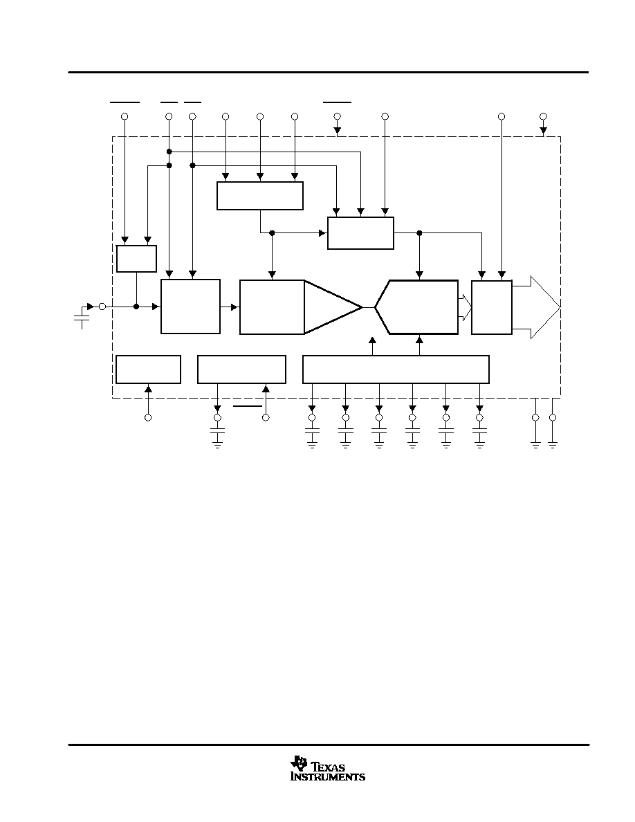
functional block diagram
Correlated
Double
Sampling
(CDS)
Programmable
Gain Amplifier
(PGA)
≠6 to
42 dB
Analog-to-Digital
Converter
Output
Latch
CCDIN
CCD
Output
Signal
Timing Control
Reference Voltage Generator
Preblanking
Input
Clamp
Optical Black (OB)
Level Clamping
Serial Interface
CLPDM
SHP SHD
SLOAD
SCLK
SDATA
RESET
ADCCK
DRVDD
VCC
12-Bit
Digital
Output
B[11:0]
PBLK
COB
CLPOB
GNDA
DRVGND
BYPP2
REFP
BYP
BYPM
REFN
CM

VSP2272
SLES020 ≠ DECEMBER 2001
4
www.ti.com
Terminal Functions
TERMINAL
TYPE (see
DESCRIPTION
NO.
NAME
TYPE (see
Note 1)
DESCRIPTION
1
B0 (LSB)
DO
A/D converter output, bit 0 (LSB)
2
B1
DO
A/D converter output, bit 1
3
B2
DO
A/D converter output, bit 2
4
B3
DO
A/D converter output, bit 3
5
B4
DO
A/D converter output, bit 4
6
B5
DO
A/D converter output, bit 5
7
B6
DO
A/D converter output, bit 6
8
B7
DO
A/D converter output, bit 7
9
B8
DO
A/D converter output, bit 8
10
B9
DO
A/D converter output, bit 9
11
B10
DO
A/D converter output, bit 10
12
B11 (MSB)
DO
A/D converter output, bit 11 (MSB)
13
DRVDD
P
Power supply for digital output
14
DRVGND
P
Digital ground for digital output
15, 17. 25, 26
35, 36, 41, 42
GNDA
P
Analog ground
16
ADCCK
DI
Clock for digital output buffer
18, 24, 27, 33, 34, 40
VCC
P
Analog power supply
19
PBLK
DI
Preblanking: High = Normal operation mode
Low = Preblanking mode: digital outputs are all 0s
20
CLPOB
DI
Optical black clamp pulse (default = active low) (see Note 5)
21
SHP
DI
CDS reference level sampling pulse (default = active low) (see Note 5)
22
SHD
DI
CDS data level sampling pulse (default = active low) (see Note 5)
23
CLPDM
DI
Dummy pixel clamp pulse (default = active low) (see Note 5)
28
COB
AO
Optical black clamp loop reference (bypass to ground) (see Note 2)
29
BYPP2
AO
Internal reference P (bypass to ground) (see Note 3)
30
CCDIN
AI
CCD signal input
31
BYP
AO
Internal reference C (bypass to ground) (see Note 4)
32
BYPM
AO
Internal reference N (bypass to ground (see Note 3)
37
CM
AO
A/D converter common mode voltage (bypass to ground) (see Note 4)
38
REFP
AO
A/D converter positive reference (bypass to ground) (see Note 4)
39
REFN
AO
A/D converter negative reference (bypass to ground) (see Note 4)
43, 44
NC
Must be left open
45
RESET
DI
Asynchronous system reset (active low)
46
SLOAD
DI
Serial data latch signal (triggered at the rising edge)
47
SDATA
DI
Serial data input
48
SCLK
DI
Clock for serial data shift (triggered at the rising edge)
NOTES:
1. Designators in TYPE: P: power supply and ground, DI: digital input, DO: digital output, AI: analog input, AO: analog output
2. Must be connected to ground with a bypass capacitor. The recommended value is 0.1
µ
F to 0.22
µ
F, however it depends on the
application environment. Refer to the optical black level clamp loop section for details.
3. Must be connected to ground with a bypass capacitor. The recommended value is 400 pF to 1000 pF, however it depends on the
application environment. Refer to the voltage reference section for details.
4. Must be connected to ground with a bypass capacitor (0.1
µ
F). Refer to the voltage reference section for details.
5. Refer to the serial interface section for details.
VSP2272
SLES020 ≠ DECEMBER 2001
5
www.ti.com
absolute maximum ratings over operating free-air temperature (unless otherwise noted)
Supply voltage: V
CC
, DRV
DD
4 V
. . . . . . . . . . . . . . . . . . . . . . . . . . . . . . . . . . . . . . . . . . . . . . . . . . . . . . . . . . . . . . . . . . . . . .
Supply voltage differences: V
CC
±
0.1 V
. . . . . . . . . . . . . . . . . . . . . . . . . . . . . . . . . . . . . . . . . . . . . . . . . . . . . . . . . . . . . . . .
Ground voltage differences: GNDA, DRV
DD
±
0.1 V
. . . . . . . . . . . . . . . . . . . . . . . . . . . . . . . . . . . . . . . . . . . . . . . . . . . . . .
Digital input voltage
≠0.3 V to 5.3 V
. . . . . . . . . . . . . . . . . . . . . . . . . . . . . . . . . . . . . . . . . . . . . . . . . . . . . . . . . . . . . . . . . . . . .
Analog input voltage
≠0.3 V to V
CC
+ 0.3 V
. . . . . . . . . . . . . . . . . . . . . . . . . . . . . . . . . . . . . . . . . . . . . . . . . . . . . . . . . . . . . .
Input current (any leads except supplies)
±
10 mA
. . . . . . . . . . . . . . . . . . . . . . . . . . . . . . . . . . . . . . . . . . . . . . . . . . . . . . . .
Operating temperature
≠25
∞
C to 85
∞
C
. . . . . . . . . . . . . . . . . . . . . . . . . . . . . . . . . . . . . . . . . . . . . . . . . . . . . . . . . . . . . . . . . .
Storage temperature
≠55
∞
C to 125
∞
C
. . . . . . . . . . . . . . . . . . . . . . . . . . . . . . . . . . . . . . . . . . . . . . . . . . . . . . . . . . . . . . . . . . .
Junction temperature
150
∞
C
. . . . . . . . . . . . . . . . . . . . . . . . . . . . . . . . . . . . . . . . . . . . . . . . . . . . . . . . . . . . . . . . . . . . . . . . . .
Lead temperature (soldering, 5 sec)
260
∞
C
. . . . . . . . . . . . . . . . . . . . . . . . . . . . . . . . . . . . . . . . . . . . . . . . . . . . . . . . . . . . .
Package temperature (IR reflow, peak, 10 sec)
235
∞
C
. . . . . . . . . . . . . . . . . . . . . . . . . . . . . . . . . . . . . . . . . . . . . . . . . . . .
Stresses beyond those listed under "absolute maximum ratings" may cause permanent damage to the device. These are stress ratings only, and
functional operation of the device at these or any other conditions beyond those indicated under "recommended operating conditions" is not
implied. Exposure to absolute-maximum-rated conditions for extended periods may affect device reliability.
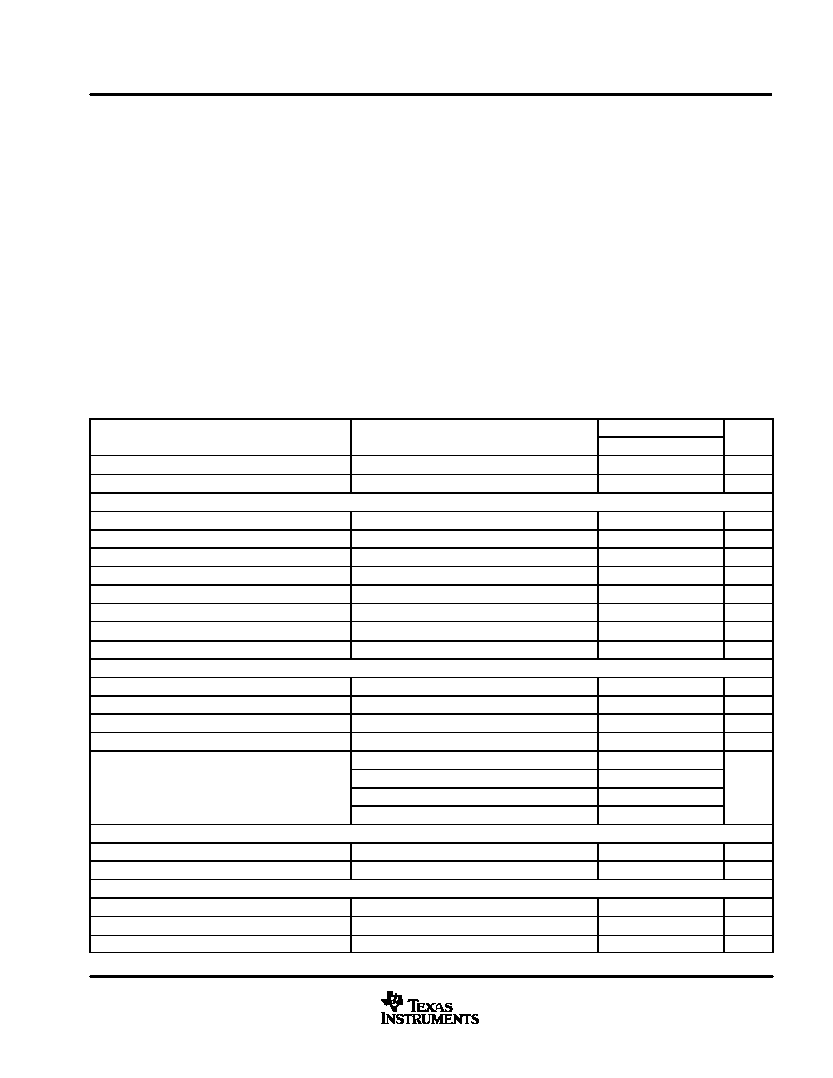
electrical characteristics all specifications at T
A
= 25
∞
C, V
CC
= 3 V, DRV
DD
= 3 V, conversion rate
(f
ADCCK
) = 20 MHz (unless otherwise noted)
PARAMETER
TEST CONDITIONS
VSP2272Y, VSP2272M
UNIT
PARAMETER
TEST CONDITIONS
MIN
TYP
MAX
UNIT
Resolution
12
Bits
Maximum conversion rate
28
MHz
DIGITAL INPUTS
Logic family
TTL
VT+
Input low-to-high threshold voltage
1.7
V
VT≠
Input high-to-low threshold voltage
1
V
IIH
Input logic high current
VI = 3 V
±
20
µ
A
IIL
Input logic low current
VI = 0 V
±
20
µ
A
ADCCK clock duty cycle
50%
Input capacitance
5
pF
Maximum input voltage
≠ 0.3
5.3
V
DIGITAL OUTPUTS
Logic family
CMOS
Logic coding
Straight binary
VOH
Output logic high voltage
IOH =
≠
2 mA
2.4
V
VOL
Output logic low voltage
IOL = 2 mA
0.4
V
J[1:0] = 00
0
Additional output data delay
J[1:0] = 01
5
ns
Additional output data delay
J[1:0] = 10
10
ns
J[1:0] = 11
13
REFERENCE
Positive reference voltage
1.75
V
Negative reference voltage
1.25
V
ANALOG INPUT (CCDIN)
Input signal level for full-scale out
PGA gain = 0 dB
900
mV
Input capacitance
15
pF
Input limit
≠0.3
3.3
V