 | –≠–ª–µ–∫—Ç—Ä–æ–Ω–Ω—ã–π –∫–æ–º–ø–æ–Ω–µ–Ω—Ç: SSM3J01F | –°–∫–∞—á–∞—Ç—å:  PDF PDF  ZIP ZIP |
SSM3J01F
2003-03-27
1
TOSHIBA Field Effect Transistor Silicon P Channel MOS Type
SSM3J01F
High Speed Switching Applications
∑ Small package
∑ Low on resistance : Ron = 0.4 (max) (V
GS
= -4 V)
: Ron = 0.6 (max) (V
GS
= -2.5 V)
∑ Low gate threshold voltage
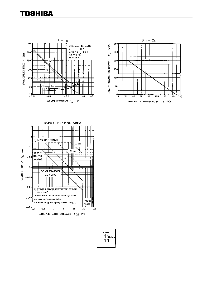
Maximum Ratings
(Ta
=
=
=
=
25∞C)
Characteristics Symbol
Rating
Unit
Drain-source voltage
V
DS
-
30 V
Gate-source voltage
V
GSS
±
10 V
DC I
D
-
700
Drain current
Pulse I
DP
-
1400
mA
Drain power dissipation (Ta
=
25∞C)
P
D
200 mW
Channel temperature
T
ch
150 ∞C
Storage temperature range
T
stg
-
55~150 ∞C
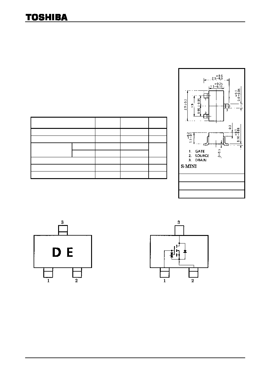
Marking
Equivalent
Circuit
Handling Precaution
When handling individual devices (which are not yet mounting on a circuit board), be sure that the environment
is protected against electrostatic electricity. Operators should wear anti-static clothing, and containers and other
objects that come into direct contact with devices should be made of anti-static materials.
Unit: mm
JEDEC TO-236MOD
JEITA SC-59
TOSHIBA 2-3F1F
Weight: 0.012 g (typ.)
SSM3J01F
2003-03-27
2
Electrical Characteristics
(Ta
=
=
=
=
25∞C)
Characteristics Symbol Test
Condition Min
Typ.
Max
Unit
Gate leakage current
I
GSS
V
GS
=
±
10 V, V
DS
=
0
æ
æ
±
1
m
A
Drain-source breakdown voltage
V
(BR) DSS
I
D
=
-
1 mA, V
GS
=
0
-
30
æ
æ
V
Drain cut-off current
I
DSS
V
DS
=
-
30 V, V
GS
=
0
æ
æ
-
1
m
A
Gate threshold voltage
V
th
V
DS
=
-
3 V, I
D
=
-
0.1 mA
-
0.6
æ
-
1.1
V
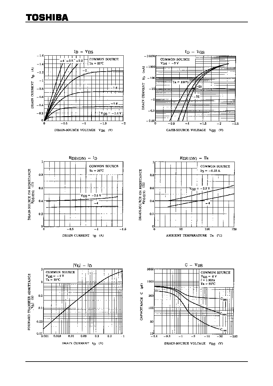
Forward transfer admittance
Ô
Y
fs
Ô
(Note)
V
DS
=
-
3 V, I
D
=
-
0.35 A
1.0
æ
æ
S
I
D
=
-
0.35 A, V
GS
=
-
4 V
æ
0.3 0.4
Drain-source ON resistance
R
DS (ON )
(Note) I
D
=
-
0.35 A, V
GS
=
-
2.5 V
æ
0.4 0.6
W
Input capacitance
C
iss
V
DS
=
-
10 V, V
GS
=
0, f
=
1 MHz
æ
240
æ
pF
Reverse transfer capacitance
C
rss
V
DS
=
-
10 V, V
GS
=
0, f
=
1 MHz
æ
24
æ
pF
Output capacitance
C
oss
V
DS
=
-
10 V, V
GS
=
0, f
=
1 MHz
æ
94
æ
pF
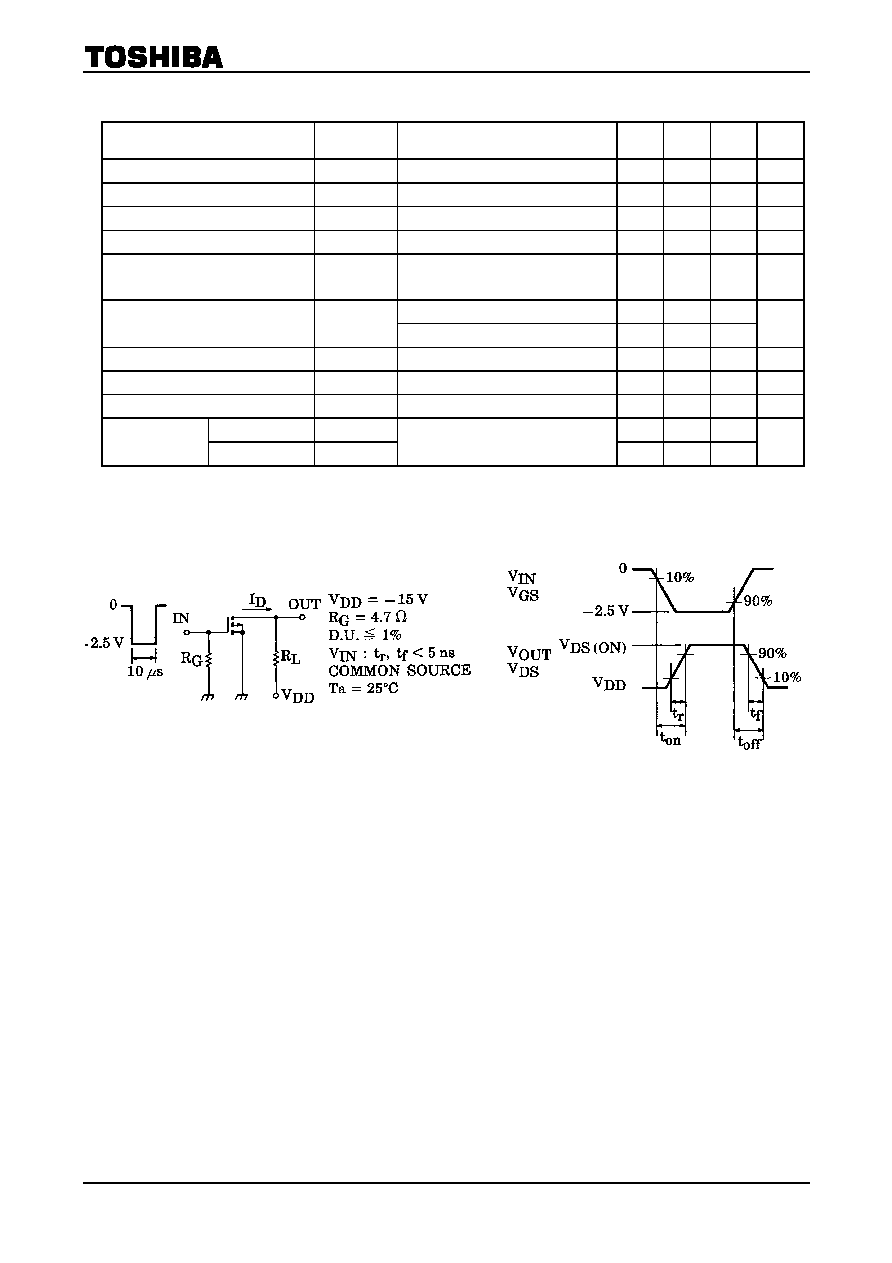
Turn-on time
t
on
æ
36
æ
Switching time
Turn-off time
t
off
V
DD
=
-
15 V, I
D
=
-
0.3 A,
V
GS
=
0~
-
2.5 V, R
G
=
4.7
W
æ
37
æ
ns
Note: Pulse test
Switching Time Test Circuit
Precaution
V
th
can be expressed as voltage between gate and source when low operating current value is I
D
=
-100 mA for
this product. For normal switching operation, V
GS (ON)
requires higher voltage than V
th
and V
GS (off)
requires
lower voltage than V
th
.
(Relationship can be established as follows: V
GS (off)
< V
th
< V
GS (ON)
)
Please take this into consideration for using the device.
V
GS
recommended voltage of -2.5 V or higher to turn on this product.
SSM3J01F
2003-03-27
3
SSM3J01F
2003-03-27
4
Figure 1 25.4 mm
¥
¥
¥
¥
25.4 mm
¥
¥
¥
¥
1.6 t (a Cu pad of 0.8 mm
2
area)

SSM3J01F
2003-03-27
5
∑
TOSHIBA is continually working to improve the quality and reliability of its products. Nevertheless, semiconductor
devices in general can malfunction or fail due to their inherent electrical sensitivity and vulnerability to physical
stress. It is the responsibility of the buyer, when utilizing TOSHIBA products, to comply with the standards of
safety in making a safe design for the entire system, and to avoid situations in which a malfunction or failure of
such TOSHIBA products could cause loss of human life, bodily injury or damage to property.
In developing your designs, please ensure that TOSHIBA products are used within specified operating ranges as
set forth in the most recent TOSHIBA products specifications. Also, please keep in mind the precautions and
conditions set forth in the "Handling Guide for Semiconductor Devices," or "TOSHIBA Semiconductor Reliability
Handbook" etc..
∑
The TOSHIBA products listed in this document are intended for usage in general electronics applications
(computer, personal equipment, office equipment, measuring equipment, industrial robotics, domestic appliances,
etc.). These TOSHIBA products are neither intended nor warranted for usage in equipment that requires
extraordinarily high quality and/or reliability or a malfunction or failure of which may cause loss of human life or
bodily injury ("Unintended Usage"). Unintended Usage include atomic energy control instruments, airplane or
spaceship instruments, transportation instruments, traffic signal instruments, combustion control instruments,
medical instruments, all types of safety devices, etc.. Unintended Usage of TOSHIBA products listed in this
document shall be made at the customer's own risk.
∑
The information contained herein is presented only as a guide for the applications of our products. No
responsibility is assumed by TOSHIBA CORPORATION for any infringements of intellectual property or other
rights of the third parties which may result from its use. No license is granted by implication or otherwise under
any intellectual property or other rights of TOSHIBA CORPORATION or others.
∑
The information contained herein is subject to change without notice.
000707EAA
RESTRICTIONS ON PRODUCT USE