 | –≠–ª–µ–∫—Ç—Ä–æ–Ω–Ω—ã–π –∫–æ–º–ø–æ–Ω–µ–Ω—Ç: TA1322FN | –°–∫–∞—á–∞—Ç—å:  PDF PDF  ZIP ZIP |
TA1322FN
2002-02-12
1
TOSHIBA Bipolar Linear Integrated Circuit Silicon Monolithic
TA1322FN
Down-Converter IC with PLL for Satellite Tuner
The TA1322FN is a wideband down-converter which can
operate at input frequency ranging from 850 MHz to 2200 MHz.
Intended primarily for use in satellite tuners, this IC includes an
oscillator, a mixer, an IF amplifier and a PLL.
The I
2
C bus data format is used as the data control format.
The supply voltage of 5.0 V helps minimize the tuner's power
dissipation, while the compact 30-pin SSOP package allows the
tuner to be kept small.
Features
∑ Supply voltage: 5.0 V (typ.)
∑ Wide input frequency range
∑ Low phase noise oscillator
∑ Standard I
2
C bus format control
∑ 4-MHz (X'tal) buffer output pin
∑ Reference oscillator input change-over switch [X'tal or external input]
∑ 33-V high-voltage tuning amplifier built-in
∑ Built-in comparator (P4, P5, P7)
∑ Bandswitch drive transistor (P0) [IBD = 40 mA (max)]
∑ Selected IF output port
∑ Frequency step: 62.5 kHz or 125 kHz (for 4-MHz X'tal)
∑ 4-address setting via address selector
∑ Power-on reset circuit
∑ ◊1/2 prescaler
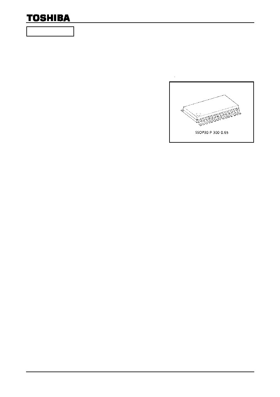
∑ Flat compact package: SSOP30-P-300-0.65 (0.65-mm pitch)
Power-On Reset Operation Conditions
∑ Frequency step: 125 kHz
∑ Charge pump output current: ±50 µA
∑ Counter data: all [0]
∑ Band driver: OFF
∑ Tuning amplifier: OFF
∑ IF output operation: pin 19 is ON
Note 1: This device can easily be damaged by high voltages or electrical fields. For this reason, please handle it
with care.
Weight: 0.17 g (typ.)
Preliminary
TA1322FN
2002-02-12
2
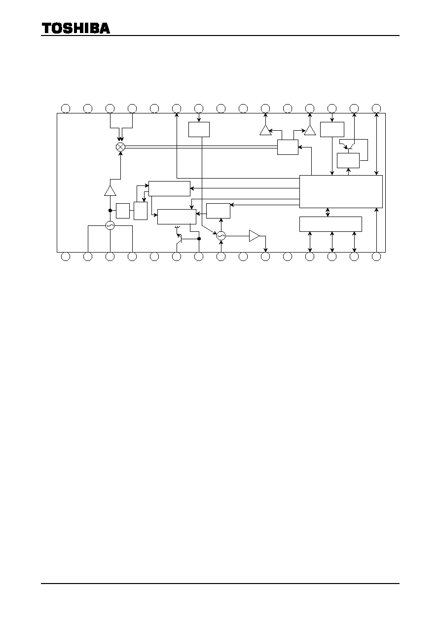
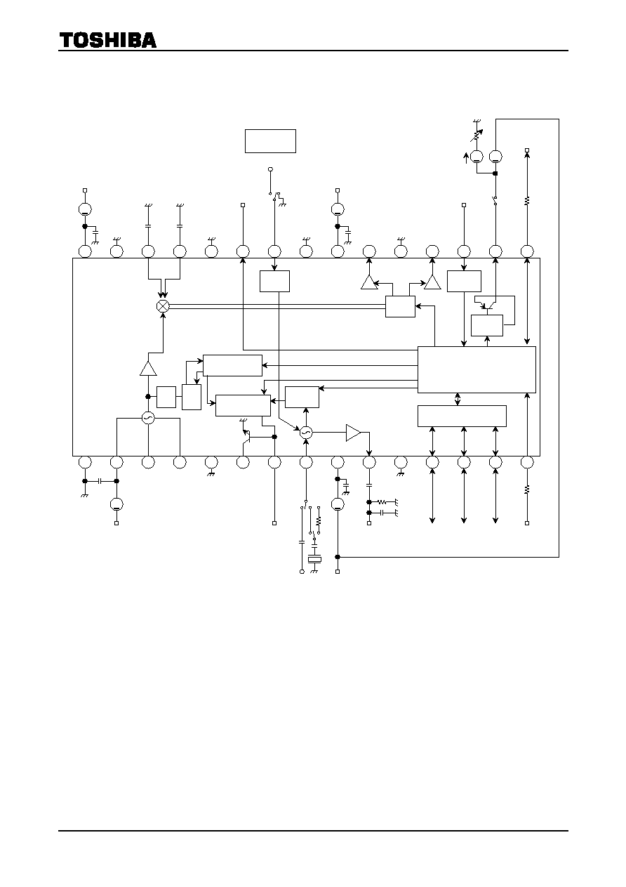
Block Diagram
Comparator
I
2
C BUS
Data Interface
Band
Driver
Phase
Comparator
Programmable
Counter
Divider
XO-SW
1/2
IF-SW
Address
1
GND1
2
V
CC
1
3
OS
C-E
4
OS
C-B
5
GND2
6
Vt-
o
u
t
7
NF
8
X'ta
l
9
V
CC
2
10
X
O
buf
f
ou
t
11
GND3
12
P4
13
P5
14
P7
15
SC
L
in
30
29
28
27
26
25
24
23
22
21
20
19
18
17
16
V
CC
4
GND7
RF i
n2
RF i
n1
GND6
TES
T
XO
SW
GND5
V
CC
3
IF o
u
t2
GND4
IF o
u
t1
AD
R
se
t
P
O
out
S
D
A
i
n
/
out
1/32
1/33
TA1322FN
2002-02-12
3
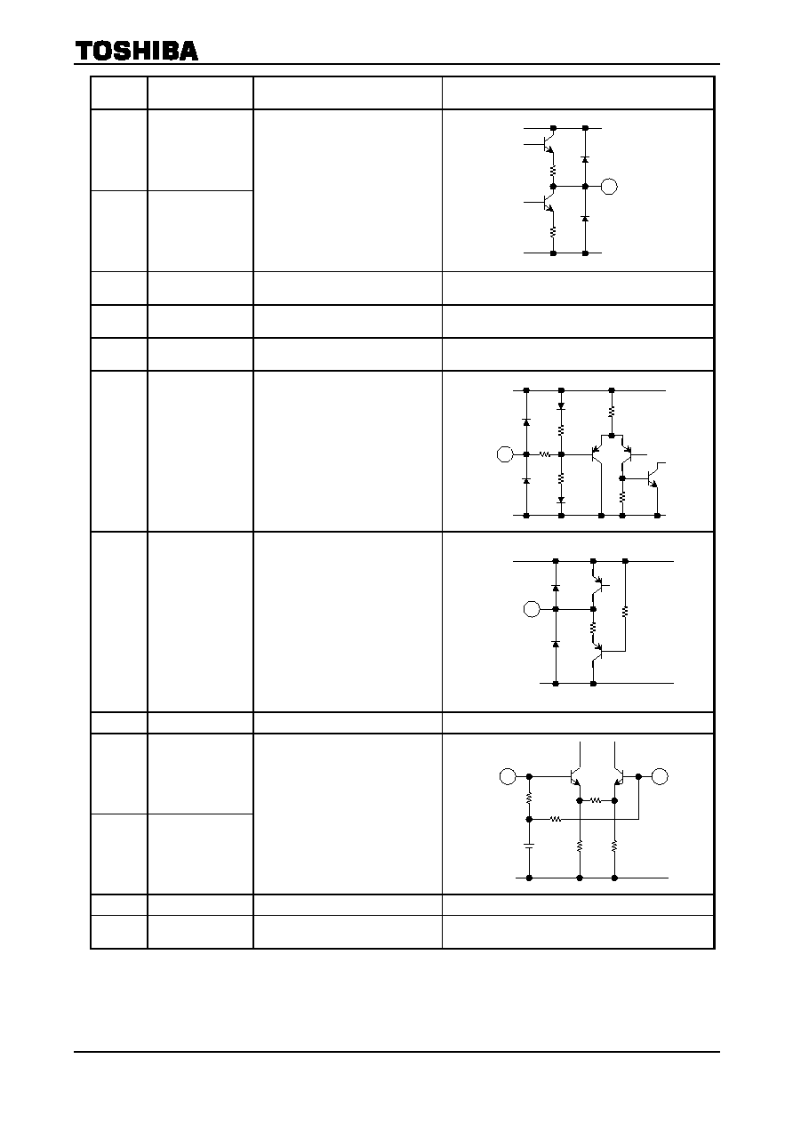
Pin Functions
Pin No.
Pin Name
Function
Interface
1
GND1
Ground pin for oscillator circuit block
æ
2
V
CC
1
Power supply pin for local oscillator
circuit block
3
4
Oscillator
Local oscillator circuit
5
GND2
Ground pin for oscillator circuit block
æ
6
Vt Output
7
NF
Tuning voltage output pin with built-in
tuning amplifier
8
Reference Input
(4-MHz input)
Crystal oscillator input
Can be switched between X'tal
oscillator and external input using pin
24 (XO switch).
9
V
CC
2
Power supply pin for PLL circuit block
æ
10
Reference signal
buffer output
Buffer output pin for reference signal
11
GND3
Ground pin for PLL circuit block
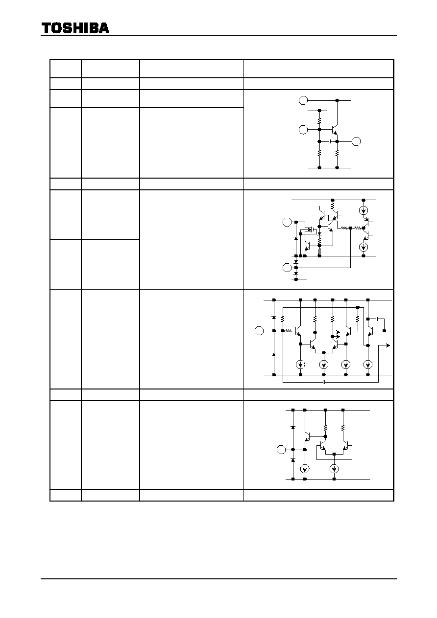
æ
2
4
3
GND1
V
CC
2
8
GND3
1 k
W
5 k
W
5 k
W
1 k
W
V
CC
2
10
GND3
5 k
W
5 k
W
6
V
CC
2
GND3
7
V
CC
2
50
W
TA1322FN
2002-02-12
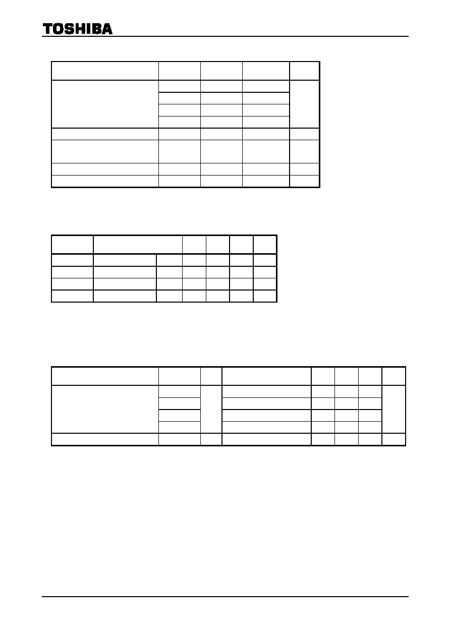
4
Pin No.
Pin Name
Function
Interface
12
P4
13
P5
14
P7
Output can be controlled by setting
the band switch data.
The circuit configuration is open
collector output.
Each pin has a built-in comparator.
The status of the comparator can be
checked READ mode.
15
SCL Input
Input pin for I
2
C bus serial clock data
16
SDA
Input/Output
Input/output pin for I
2
C bus serial
clock data
17
PO output
Output can be controlled by setting
band switch data.
18
ADR Set
The address for hardware bit setting
can be selected by applying voltage to
this pin.
4 programmable address can be
programmed.
V
CC
2
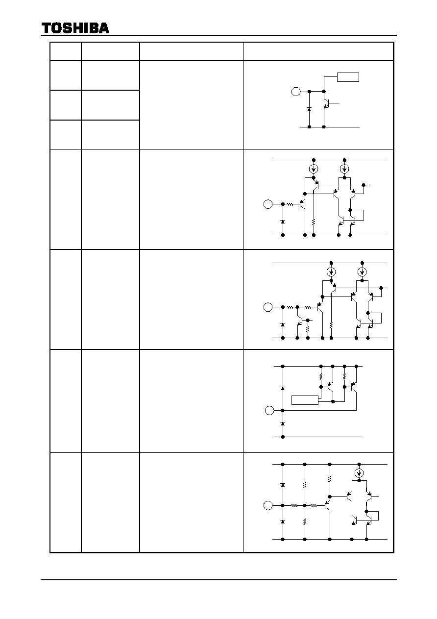
15
GND3
1 k
W
100
W
V
CC
2
16
GND3
1 k
W
100
W
20
W
70 k
W
GND3
12, 13, 14
CMOP
V
CC
2
17
GND3
DATA I/F
12 k
W
12 k
W
V
CC
2
18
GND3
50 k
W
150
k
W
100
W
1 k
W
100
W
TA1322FN
2002-02-12
5
Pin No.
Pin Name
Function
Interface
19
IF Output 1
21
IF Output 2
IF output pin.
Output can be controlled by setting
the band switch data (P6).
IF output impedance is 75
W
each
other.
When P6 data set 0, output pin is Pin
19 (IF output 1).
When P6 data set 1, output pin is Pin
21 (IF output 2).
20
GND4
Ground pin for IF amplifier circuit
block
æ
22
V
CC
3
Power supply pin for IF amplifier
circuit block
æ
23
GND5
Ground pin for IF amplifier circuit
block
æ
24
XO Switch
Determines reference signal input.
If connected to ground:
X'tal oscillator.
If open or connected to V
CC
2:
external input
25 TEST
When test mode set, this pin can
confirm X'tal divider signal and 1/2
counter signal.
This pin can be used at open.
26
GND6
Ground pin for mixer circuit block
æ
27
RF Input1
28
RF Input2
RF signal input pin
Input can be either balanced or
unbalanced.
29
GND7
Ground pin for mixer circuit block
æ
30
V
CC
4
Power supply pin for mixer circuit
block
æ
V
CC
3
GND4, 5
19, 21
V
CC
2
24
GND3
25 k
W
25
k
W
1 k
W
GND7
27
28
3 k
W
3 k
W
V
CC
2
25
GND3
25 k
W
100 k
W
TA1322FN
2002-02-12
6
Absolute Maximum Ratings
(Ta
=
=
=
=
25∞C)
Parameter Pin
No.
Symbol
Rating
Unit
2
V
CC
1
6
9
V
CC
2
6
22
V
CC
3
6
Supply voltage
30
V
CC
4
6
V
Tuning amplifier voltage
6
VBT
38
V
Power dissipation
æ
P
D
1130
(Note 2)
mW
Operating temperature
æ
T
opr
-
20 to 85
∞C
Storage temperature
æ
T
stg
-
55 to 150
∞C
Note 2: 50 mm
¥
50 mm
¥
1.6 mm, 40% Cu board
If Ta
>
25∞C, derate this value by 9.1 mW/∞C.
Recommended Operating Conditions
Pin No.
Symbol
Min
Typ.
Max
Unit
2
Local oscillator block
V
CC
1
4.5
5.0
5.5
V
9
PLL block
V
CC
2
4.5
5.0
5.5
V
22
IF amplifier block
V
CC
3
4.5
5.0
5.5
V
30
Mixer block
V
CC
4
4.5
5.0
5.5
V
Electrical Characteristics
DC Characteristics
(unless otherwise specified, V
CC
1
=
=
=
=
V
CC
2
=
=
=
=
V
CC
3
=
=
=
=
V
CC
4
=
=
=
=
5 V, Ta
=
=
=
=
25∞C)
When power on, counter data
=
=
=
=
all [0], VBT
=
=
=
=
OFF, CP0
=
=
=
=
0, band
=
=
=
=
all [0], and IF output
operate Pin 19.
Parameter Symbol
Test
Circuit
Test Condition
Min
Typ.
Max
Unit
I
CC
1
æ
5.0
7.5
9.5
I
CC
2
æ
21.5
26.5
32.0
I
CC
3
æ
19.5
24.0
29.0
Power supply current
I
CC
4
1
æ
10.0
12.5
15.5
mA
Total
I
CC
-total
æ
æ
56.0
70.0
86.0
mA
TA1322FN
2002-02-12
7
Down-Converter Block
AC Characteristics
(unless otherwise specified, V
CC
1
=
=
=
=
V
CC
2
=
=
=
=
V
CC
3
=
=
=
=
V
CC
4
=
=
=
=
5 V, Ta
=
=
=
=
25∞C)
Parameter Symbol
Test
Circuit
Test Condition
(Note 4, Note 5)
Min Typ. Max
Unit
RF input frequency
Mfin
æ
æ
850
æ
2200
MHz
RF input level
MPin
æ
æ
æ
æ
-
35
dBmW
IF output frequency
Afin
æ
æ
350
æ
550
MHz
IF output impedance
(Note 3)
AZout
æ
Single-end
æ
75
æ
W
Local oscillator frequency
LO
æ
æ
1300
æ
2700
MHz
fRF
=
898 MHz
27.5
30.5
33.5
fRF
=
1598 MHz
27
31
34
Conversion gain
(Note 3)
CG 3
fRF
=
2198 MHz
24.5
29
32
dB
fRF
=
898 MHz
æ
9 10.5
fRF
=
1598 MHz
æ
9 11.5
Noise figure
(Note 3)
NF 4
fRF
=
2198 MHz
æ
11 13
dB
fRF
=
898 MHz
6
8
æ
fRF
=
1598 MHz
6
8
æ
IF output power level
(Note 3)
Apsat 3
fRF
=
2198 MHz
6
8
æ
dBmW
fd
=
898 MHz, fud
=
903 MHz
13
15
æ
fd
=
1598 MHz,
fud
=
1603 MHz
14 16
æ
3
rd
inter modulation
(IF output intercept point)
(Note 3)
IP3 5
fd
=
2198 MHz,
fud
=
2203 MHz
14 16
æ
dBmW
fRF
=
898 MHz
æ
æ
±
2
fRF
=
1598 MHz
æ
æ
±
2
Conversion gain shift
(Note 3)
CGs 3
fRF
=
2198 MHz
æ
æ
±
2
dB
fosc
=
1300 MHz
æ
æ
±
5.5
fosc
=
2000 MHz
æ
æ
±
3.5
Frequency shift
(PLL OFF)
D
fB 3
fosc
=
2600 MHz
æ
æ
±
3.5
MHz
fosc
=
1300 MHz
æ
-
74
-
70
fosc
=
2000 MHz
æ
-
75
-
71
Phase noise
(with 10-kHz offset)
PN 3
fosc
=
2600 MHz
æ
-
74
-
70
dBc/
Hz
fosc
=
1300 MHz
æ
-
36
-
33
fosc
=
2000 MHz
æ
-
31.5
-
28
RF pin
LO leak level
LORF 3
fosc
=
2600 MHz
æ
-
33
-
30
dBmW
fosc
=
1300 MHz
æ
-
21.5
-
15.5
fosc
=
2000 MHz
æ
-
31
-
25
IF pin
LO leak level
LOIF 3
fosc
=
2600 MHz
æ
-
36
-
30.5
dBmW
fRF
=
898 MHz
30
36
æ
fRF
=
1598 MHz
30
36
æ
IF switch isolation
IFiso
3
fRF
=
2198 MHz
30
36
æ
dB
Note 3: IF output frequency
=
402 MHz
Note 4: IF output load
=
75
W
Note 5: IF output operate Pin 21
TA1322FN
2002-02-12
8
PLL Block
(unless otherwise specified, V
CC
1
=
=
=
=
V
CC
2
=
=
=
=
V
CC
3
=
=
=
=
V
CC
4
=
=
=
=
5 V, Ta
=
=
=
=
25∞C)
Parameter Symbol
Test
Circuit
Test Condition
Min Typ. Max
Unit
Tuning amplifier output voltage (close)
Vt out
1
VBT
=
33 V, RL
=
33 k
W
0.3
æ
33
V
Tuning amplifier maximum current
Ivt
1
VBT
=
33 V
æ
æ
3
mA
X'tal negative resistance
XtR
1
1
2.5
æ
k
W
X'tal operating frequency
OSCin
1
XO-SW:GND (X'tal oscillator
mode)
[NDK (AT-51), 4 MHz used]
3.2
æ
4.5
MHz
X'tal external input level
Xo extl
1
100
æ
1000
mV
p-p
X'tal external input frequency
X-ext
1
XO-SW: V
CC
2 or open
2
æ
6
MHz
Ratio setting range
N
æ
15-bit counter
1024
æ
32767
Logic input low voltage
V
IL
1
-
0.3
æ
1.5
V
Logic input high voltage
V
IH
1
SDA and SCL pins
3
æ
V
CC
2
+
0.3
V
Logic input current (low)
I BsL
1
-
20
æ
10
m
A
Logic input current (high)
I BsH
1
SDA and SCL pins
-
10
æ
20
m
A
ACK output voltage
VACK
1
ISINK
=
3 mA
æ
æ
0.4
V
CP
=
[0]
±
35
±
50
±
75
Charge pump output current
Ichg
1
CP
=
[1]
±
180
±
240
±
345
m
A
Band driver drive current
IBD
1
P0
æ
æ
40
mA
Band driver voltage drop
VBDsat
1
P0: IBD
=
40-mA drive
æ
0.2
0.4
V
Comparator pin input voltage
VCMP
1
IP4, IP5, IP7
0
æ
6
V
Comparator pin low voltage
VLCMP
1
IP4, IP5, IP7
0
æ
1.5
V
Comparator pin high voltage
VHCMP
1
IP4, IP5, IP7
2.7
æ
6
V
Output port flow current
IPin
2
P4, P5, P7
æ
æ
7 mA
Output port saturation voltage
Vpinsat
2
P4, P5, P7 (Ipin
=
7 mA)
æ
0.1
0.15
V
Output port leakage current
Iplk
1
P4, P5, P7 (Vport
=
6 V)
æ
æ
10
m
A
Output port maximum voltage
Vport
1
P4, P5, P7
æ
æ
6 V
Xo buffer output level
Xo out
1
1-k
W
, 10-pF load
X'tal: NDK (AT-51), 4 MHz
used.
4-MHz level monitored on
oscilloscope using FET probe
(1 M
W
, 1.9 pF).
350
500
æ
mV
p-p

TA1322FN
2002-02-12
9
Bus Line Characteristics
Parameter Symbol
Test
Circuit
Test Condition
Min
Typ.
Max
Unit
SCL clock frequency
fSCL
0
æ
100
kHz
Bus free time between a STOP and
START conditions
t
BUF
4.7
æ
æ
m
s
Hold time for repeated START
condition
t
HD
; STA
4
æ
æ
m
s
SCL clock low period
t
LOW
4.7
æ
æ
m
s
SCL clock high period
t
HIGH
4
æ
æ
m
s
Set-up time for repeated START
condition
f
SU
; STA
4.7
æ
æ
m
s
Data hold time
t
HD
; DAT
0
æ
æ
m
s
Data set-up time
t
SU
; DAT
250
æ
æ
ns
Rise time for SDA and SCL signals
tR
æ
æ
1000
ns
Fall time for SDA and SCL signals
tF
æ
æ
300
ns
Set-up time for STOP condition
tsU; STO
æ
Please refer to data timing
chart.
4
æ
æ
m
s
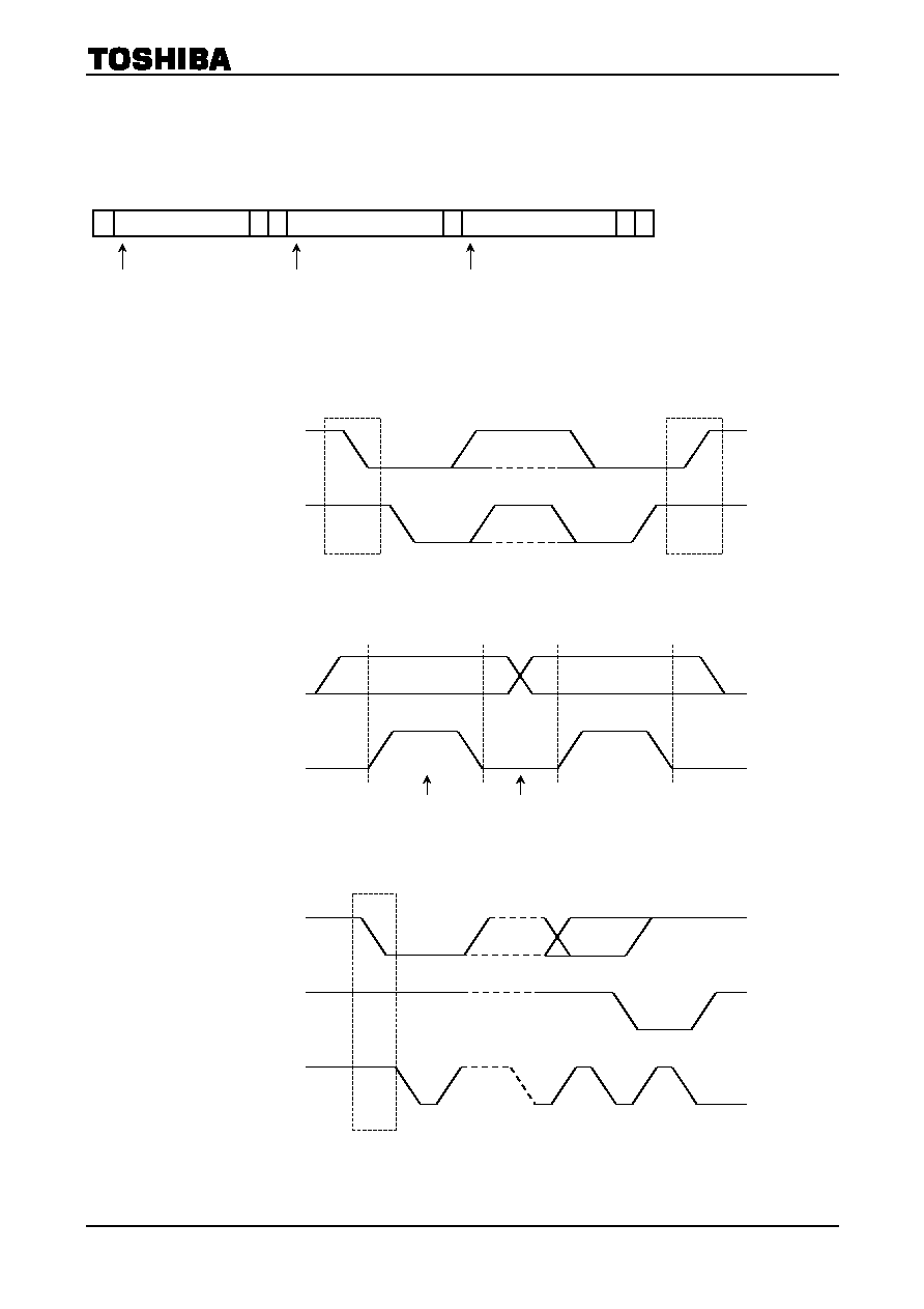
t
HD
; STA
tSU; STO
SDA
SCL
t
BUF
t
LOW
tR
tF
t
HD
; STA
t
HD
; DAT
t
HIGH
t
SU
; DAT t
SU
; STA
P S
Sr
P
Figure 1 I
2
C Bus Data Timing Chart (rising-edge timing)

TA1322FN
2002-02-12
10
Test Conditions
(1) Conversion
gain
RF input level = -40dBmW
(2) Noise
figure
NF meter direct-reading value (DSB measurement)
(3) IF output power level
Measure maximum IF output level.
(4) 3rd inter modulation
∑ fd (fd input level = -40dBmW)
∑ fud = fd + 5 MHz (fud input level = -40dBmW)
Calculate IF output intercept point as follows:
IP3 = S/(N - 1) + P [dBmW]
S: suppression level
N: 3 P: IF output level
(5) Conversion gain shift
Conversion gain shift is defined as change in conversion gain when supply voltage exceeds ranges
V
CC
= 5 V to 4.5 V or V
CC
= 5 V to 5.5 V.
(6) Frequency shift (PLL OFF)
Frequency shift is defined as change in oscillator frequency when supply voltage exceeds ranges
V
CC
1 = 5 V to 4.5 V or V
CC
1 = 5 V to 5.5 V.
(7) Phase
noise
(offset
= 10 kHz)
Measure phase noise at 10-kHz offset.
(8) RF pin local-leak level
Measure worst-case local-leak level for RF pin (with IF output pin open).
(9) IF pin local-leak level
Measure worst-case local-leak level for IF pin (with RF input pins shorted using 50-W resistor, and
not measure IF output pin open).
(10) IF switch isolation
RF input level = -40dBmW
Measure selected IF output pin's level, and not selected IF output pin's level.
Ifiso = |(selected IF output pin's level ) - (not selected IF output pin's level)|
Not selected IF output pin shorts using 50 W resistor.

TA1322FN
2002-02-12
11
PLL Block
--I
2
C Bus Communications Control--
The TA1322FN conforms to Standard Mode I
2
C bus format.
I
2
C Bus Mode allows two-way bus communication using Write Mode (for receiving data) and Read Mode (for
processing status data).
Write Mode or Read Mode can be selected by setting the least significant bit (R/W bit) of the address byte.
If the least significant address bit is set to 0, Write Mode is selected; if it is set to 1, Read Mode is selected.
Address can be set using the hardware bits. 4 programmable address can be programmed.
Using this setting, multiple frequency synthesizers can be used on the same I
2
C bus line.
The address for the hardware bit setting can be selected by applying voltage to the address setting pin (ADR-pin
18). The address is selected according to the setting of these bits.
During acknowledgment of receipt of a valid address byte, the serial data (SDA) line is Low.
If Write Mode is currently selected, when the data byte is programmed, the serial data (SDA) line will be Low
during the next acknowledgment.
A) Write mode (setting command)
When Write Mode is selected, byte 1 holds address data; byte 2 and byte 3 hold frequency data; byte
4 holds the divider ratio setting and function setting data; and byte 5 holds output port data.
Data is latched and transferred at the end of byte 3, byte 4 and byte 5.
Byte 2 and byte 3 are latched and transferred as a byte pair.
Once a valid address has been received and acknowledged, the data type can be determined by
reading the first bit of the next byte. That is, if the first bit is 0, the data is frequency data; if it is 1,
the data is function-setting or band output data.
Additional data can be input without the need to transmit the address data again until the I
2
C bus
STOP condition is detected (e.g. a frequency sweep using additional frequency data is possible).
If a data transmission is aborted, data programmed before the abort remains valid.
[[BYTE 1]]
The address data for byte 1 can be set using the hardware bit.
The hardware bit can be set by applying a voltage to the address-setting pin (ADR: pin 18).
[[BYTE 2, BYTE 3]]
Byte 2, byte 3 control the 15-bit programmable counter ratio and are stored in the 15-bit shift
register together with frequency setting counter data.
The program frequency can be calculated using the following formula:
fosc = 2 ¥ fr ¥ N
fosc: Program frequency
fr: Phase comparator reference frequency
N: Counter total divider ratio
fr is calculated from the crystal oscillator frequency and the reference frequency divider ratio
set in byte 4 (the control byte).
(fr = X'tal oscillator frequency/reference divider ratio)
The reference frequency divider ratio can be set to 1/64 or 1/128.
When a 4-MHz crystal oscillator is used, fr = 62.5 kHz or 31.25 kHz. The respective step
frequencies are 125 kHz and 62.5 kHz.
[[BYTE 4]]
Byte 4 is a control byte used to set function. Bit 2 (CP) controls the output current of the
charge-pump circuit.
When bit 2 is set to [0], the output current is set to ±50 mA; when set to [1], ±240 mA.
Bit 3 (T1) is used to set the test mode. When bit 3 is set to [0], normal mode; when set to [1],
test mode.
Bit 4 (T0) is used to set the charge pump. When bit 4 is set to [0], charge pump is ON (normal
used); When set to [1], charge pump is OFF.
Bit 5 (TS2) and bit 6 (TS1) used to set the test mode. They are used to set the charge pump test,
phase comparator reference signal output, and 1/2 counter divider ratios.
Bit 7 (TS0) is used to set the X'tal reference frequency divider ratio. When bit 7 is set to [0],
1/128 (frequency step is 62.5 kHz); when set to [1], 1/64 (frequency step is 125 kHz).
Bit 8 (OS) is used to set the charge pump drive amplifier output setting. When bit 8 is set to [0],
TA1322FN
2002-02-12
12
the output is ON (normal mode); when set to [1], the output is OFF.
[[BYTE 5]]
Byte 5 can be used to set control the output port.
Bit 1 (P7), bit 3 (P5) and bit 4 (P4) are used to control output port P7, P5 and P4.
Bit 2 (P6) is used to control change IF output port. When bit 2 is set to [0], IF output 1 (pin 19)
is ON; when set to [1], IF output 1 (pin 21) is ON.
Bit 8 (P0) is used to control band output port (P0). When bit 8 is set to [0], P0 is OFF; when set
to [1], P0 is ON. (P0) output port can be driven at less than 40 mA.
B) READ mode (status request)
When READ mode is set, power-on reset operation status, phase comparator lock detector output
status, comparator input voltage status are output to the master device.
Bit 1 (POR) indicates the power-on reset operation status. When the power supply of V
CC
2 stops,
bit is set to [1]. The condition for reset to [0], voltage supplied to V
CC
2 is 3 V or higher, transmission
is requested in READ mode, and the status is output. (when V
CC
2 is turned on, bit 1 is also set to [1].)
Bit 2 (FL) indicates the phase comparator lock status. When locked, [1] is output; when unlocked,
[0] is output.
Bit 3 (IP7), bit 4 (IP5) and bit 5 (IP4) indicate the input comparator status. High level status is
output [1], low level status is output is [0]. When voltage applied from 0 V to 1.5 V, output is [0].
When from 2.7 V to 6 V, output is [1].
Data Format
A) Write
mode
MSB
LSB
1
Address
Byte 1 1 0 0 0
MA1
MA0
R/W
=
0
ACK
2
Divider Byte 1
0
N14
N13
N12
N11
N10
N9
N8
ACK
3
Divider
Byte
2 N7 N6 N5 N4 N3 N2 N1 N0
ACK
(L)
4 Control
Byte
1
CP
T1
T0
TS2
TS1
TS0
OS ACK
(L)
5
Band
SW
Byte P7 P6 P5 P4
¥
¥
¥
P0
ACK
(L)
¥
: Don't care
ACK: Acknowledged
(L): Latch and transfer timing
B) Read
mode
MSB
LSB
1
Address
Byte 1 1 0 0 0
MA1
MA0
R/W
=
1
ACK
2 Status
Byte
POR
FL
IP7
IP5
IP4
1
1
1
æ
ACK: Acknowledged
TA1322FN
2002-02-12
13
Data Specifications
∑ MA1 and MA0: programmable hardware address bits
MA1
MA0
Voltage Applied to Address Pin
0
0
0 to 0.1V
CC
2
0
1
OPEN or 0 to V
CC
2
1
0
0.4V
CC
2 to 0.6V
CC
2
1
1
0.9V
CC
2 to V
CC
2
∑ N14-N0: programmable counter data
∑ CP: charge pump output current setting
[0]: ±50 mA (typ.)
[1]: ±240 mA (typ.)
∑ T1: test mode setting
[0]: normal mode
[1]: test mode
∑ T0: charge pump setting
[0]: charge pump is ON (normal mode)
[1]: charge pump is OFF
∑ TS0: X'tal reference frequency divider ratio select bits.
TS0
Divider ratio
Step frequency
fr
0
1/128
62.5 kHz
31.25 kHz
1
1/64 125
kHz
62.5 kHz
∑ T1, TS2, TS1, TS0: test mode
Characteristics
T1
TS2
TS1
TS0
Divider ratio
Notes
Normal operation
0
¥
¥
0 1/128
æ
Normal operation
0
¥
¥
1
1/64
æ
Sink 1
1
0 0 1/128
æ
Charge pump
Source 1
1
0 1
1/64
æ
Output port OFF
1
1
1
0 1/128
P7,
P5,
P4
OFF
Phase comparator test
1
1
1
1
1/64
SDA: Comparative signal input
SCL: Reference signal input
1
0 0 0 1/128
X'tal divider counter output
1
0 0 1
1/64
Output to pin 25 (TEST)
1
0 1
0 1/128
1/2 counter divider output
1
0 1
1
1/64
Output to pin 25 (TEST)
¥
: DON'T CARE
Note 5: When test mode, OS
=
0 (tuning ON) is necessary.
When testing the counter divider output, programmable counter data input is necessary.

TA1322FN
2002-02-12
14
∑ OS: tuning amplifier control setting
[0]: Tuning amplifier ON (normal operation)
[1]: Tuning amplifier OFF
∑ P4, P5, P7: output port
[0]: OFF
[1]: ON
∑ P6: IF output port switchover
P6 Output
Port
0
IF output 1 (pin 19) is ON
1
IF output 2 (pin 21) is ON
∑ P0: band output
[0]: OFF
[1]: ON
This can be driven at less than 40 mA.
∑ POR: power-on reset flag
[0]: normal operation
[1]: reset operation
∑ FL: lock detect flag
[0]: Unlocked
[1]: Locked
∑ IP4, IP5, IP7: comparator output
[0]: supply voltage is from 0 V to 1.5 V
[1]: supply voltage is from 2.7 V to 6 V
∑ XO-SW: reference signal input changeover
Pin 24
Input Method
GND
X'tal
V
CC
2 or open
External input
TA1322FN
2002-02-12
15
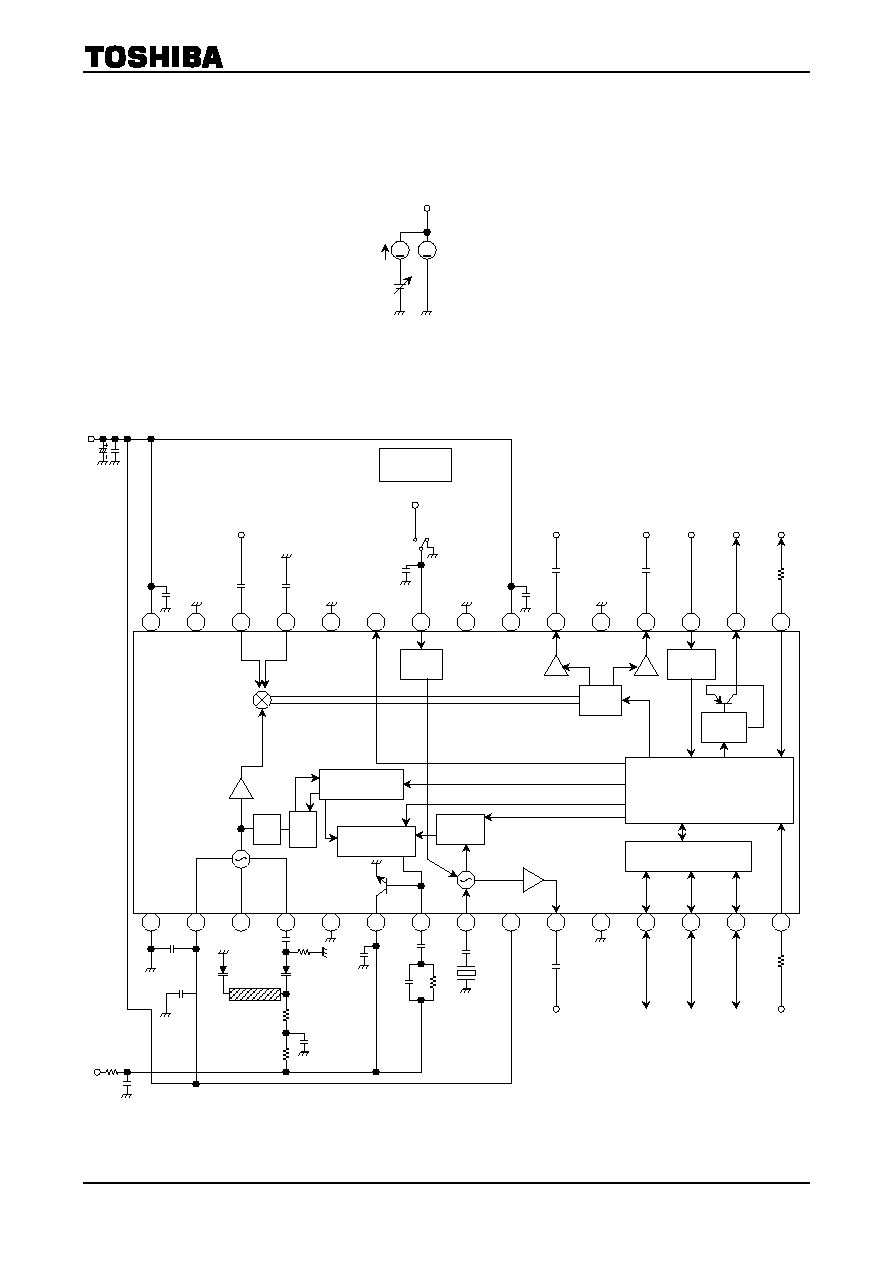
Test Circuit 1
DC Characteristics
X'tal: NDK (AT-51), 4 MHz
1
2
3
4
5
6
7
8
9
10
11
12
13
14
30
29
28
27
26
25
24
23
22
21
20
19
18
17
16
Comparator
I
2
C BUS
Data Interface
Band
Driver
Phase
Comparator
Programmable
Counter
Divider
XO-SW
1/2
0.01
m
F
V
CC
1 (5 V)
NF
NC NC
NC
I
CC
1
P5
P4
SCL
P7
4 MHz out
V
CC
2 (5 V)
1 nF
10 pF
1 k
W
0.
01
m
F
A
I
CC
2
A
EXT.in
1 nF
22 pF
*
X'
ta
l
SDA
TEST
V
CC
3 (5 V)
V
NC
A I
CC
3
0.
01
m
F
V
CC
4 (5 V)
A
0.
01
m
F
I
CC
4
1 nF
1 nF
VBD
sat
IBD
XO-SW
V
CC
2/Open
VCC2/Open:
Extenal input
GND: X'tal
ADR set
NC
A
390
W
IF-SW
Address
390
W
15
1/32
1/33
TA1322FN
2002-02-12
16
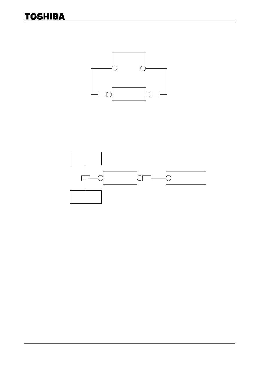
Test Circuit 2
DC Characteristics
Measurement for "Output port flow current" and "Output port saturation voltage".
Test Circuit 3
AC Characteristics
V
I
Pin
12, 13, 14
A
V
Pinsat
1
2
3
4
5
6
7
8
9
10
11
12
13
14
30
29
28
27
26
25
24
23
22
21
20
19
18
17
16
Comparator
I
2
C BUS
Data Interface
Band
Driver
Phase
Comparator
Programmable
Counter
Divider
XO-SW
1/2
P5
P4
SCL
P7
TEST
0.
1
m
F
0.
1
m
F
1 nF
XO-SW
V
CC
2/Open
VCC2/Open:
Extenal input
GND: X'tal
IF-SW
Address
390
W
15
1 nF
RF in
1 nF
SDA
PO
out
ADR
set
IF out 1
IF out 2
1 nF
390
W
1 nF
4 MHz out
1 nF
0.1
m
F
L
47 pF
22 pF
X'ta
l
4.
7 nF
13 k
W
0.
1
m
F
5 pF
10 k
W
4.
7 k
W
4.
7 nF
10 k
W
1T379
1T379
1 nF
47 k
W
33 V
0.1
m
F
5 V
1/32
1/33
TA1322FN
2002-02-12
17
Test Circuit 4
Measuring Noise Figure
Test Circuit 5
Measuring 3
rd
Inter Modulation
28
DUT
75
W
-50
W
impedance
transformer
Noise Figure Meter
out
in
IF output
pin
Noise source
fud
Spectrum
Analyzer
fd
Signal
Generator 2
Signal
Generator 1
28
DUT
in
75
W
-50
W
impedance
transformer
IF output
pin
TA1322FN
2002-02-12
18
I
2
C-Bus Control Summary
The bus control format of TA1322FN conforms to the Philips I
2
C-bus control format.
Data Transmission Format
S: Start condition
P: Stop condition
A: Acknowledge
(1) Start/stop
condition
(2) Bit
transfer
(3) Acknowledge
Serial Data
Serial Clock
Serial data can be changed.
Serial data unchanged.
Serial Data
Serial Clock
S
Start condition
P
Stop condition
7 bits
8 bits
8 bits
MSB
MSB
MSB
S Slave
address 0
A
SUB
address A
Data
A P
High-Impedance
Serial Data From
Master Device
S
8
1
Serial Clock
From Slave
Serial Clock From
Master Device
9
High-Impedance
TA1322FN
2002-02-12
19
(4) Slave
address
A6
A5
A4
A3
A2
A1
A0
R/W
1
1
0
0
0
*
*
0
Purchase of TOSHIBA I
2
C components conveys a license under the Philips I
2
C Patent Tights to use
these components in an I
2
C system, provided that the system conforms to the I
2
C Standard
Specification as defined by Philips.
Handling Precautions
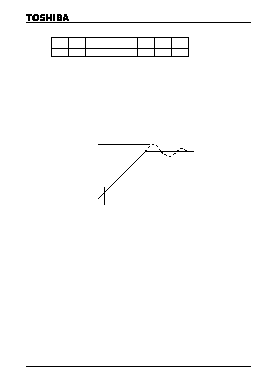
1. The device should not be inserted into or removed from the test jig while a voltage is being applied to it:
otherwise the device may be degraded or break down.
Also, do not abruptly increase or decrease the power supply to the device (see figure 1).
Overshoot or chattering in the power supply may cause the IC to be degraded.
To avoid this, filters should be placed on the power supply line.
2. The peripheral circuits described in this datasheet are given only as system examples for evaluating the
device's performance. TOSHIBA intend neither to recommend the configuration or related values of the
peripheral circuits nor to manufacture such application systems in large quantities.
Please note that the high-frequency characteristics of the device may vary depending on the external
components, the mounting method and other factors relating to the application design. Therefore, the
evaluation of the characteristics of application circuits is the responsibility of the designer.
TOSHIBA only guarantee the quality and characteristics of the device as described in this datasheet and
do not assume any responsibility for the customer's application design.
3. In order to better understand the quality and reliability of TOSHIBA semiconductor products and to
incorporate them into designs in an appropriate manner, please refer to the latest Semiconductor
Reliability Handbook (integrated circuits) published by TOSHIBA Semiconductor Company.
This handbook can also be viewed on-line at the following URL:
<http://www.semicon.toshiba.co.jp/noseek/us/sinrai/sinraifm.htm>.
1 ms
Time
10%
90%
6 V (
V
CC
1,
V
CC
2,
V
CC
3,
V
CC
4)
38 V (VBT)
S
uppl
y v
o
l
t
age
Figure 1
TA1322FN
2002-02-12
20
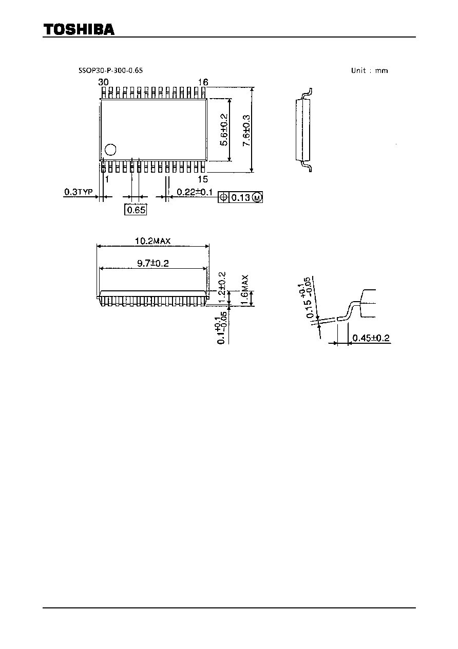
Package Dimensions
Weight: 0.17 g (typ.)

TA1322FN
2002-02-12
21
∑
TOSHIBA is continually working to improve the quality and reliability of its products. Nevertheless, semiconductor
devices in general can malfunction or fail due to their inherent electrical sensitivity and vulnerability to physical
stress. It is the responsibility of the buyer, when utilizing TOSHIBA products, to comply with the standards of
safety in making a safe design for the entire system, and to avoid situations in which a malfunction or failure of
such TOSHIBA products could cause loss of human life, bodily injury or damage to property.
In developing your designs, please ensure that TOSHIBA products are used within specified operating ranges as
set forth in the most recent TOSHIBA products specifications. Also, please keep in mind the precautions and
conditions set forth in the "Handling Guide for Semiconductor Devices," or "TOSHIBA Semiconductor Reliability
Handbook" etc..
∑
The TOSHIBA products listed in this document are intended for usage in general electronics applications
(computer, personal equipment, office equipment, measuring equipment, industrial robotics, domestic appliances,
etc.). These TOSHIBA products are neither intended nor warranted for usage in equipment that requires
extraordinarily high quality and/or reliability or a malfunction or failure of which may cause loss of human life or
bodily injury ("Unintended Usage"). Unintended Usage include atomic energy control instruments, airplane or
spaceship instruments, transportation instruments, traffic signal instruments, combustion control instruments,
medical instruments, all types of safety devices, etc.. Unintended Usage of TOSHIBA products listed in this
document shall be made at the customer's own risk.
∑
The products described in this document are subject to the foreign exchange and foreign trade laws.
∑
The information contained herein is presented only as a guide for the applications of our products. No
responsibility is assumed by TOSHIBA CORPORATION for any infringements of intellectual property or other
rights of the third parties which may result from its use. No license is granted by implication or otherwise under
any intellectual property or other rights of TOSHIBA CORPORATION or others.
∑
The information contained herein is subject to change without notice.
000707EBA
RESTRICTIONS ON PRODUCT USE