 | –≠–ª–µ–∫—Ç—Ä–æ–Ω–Ω—ã–π –∫–æ–º–ø–æ–Ω–µ–Ω—Ç: TA31273FN | –°–∫–∞—á–∞—Ç—å:  PDF PDF  ZIP ZIP |
TA31273FN
2002-07-08
1
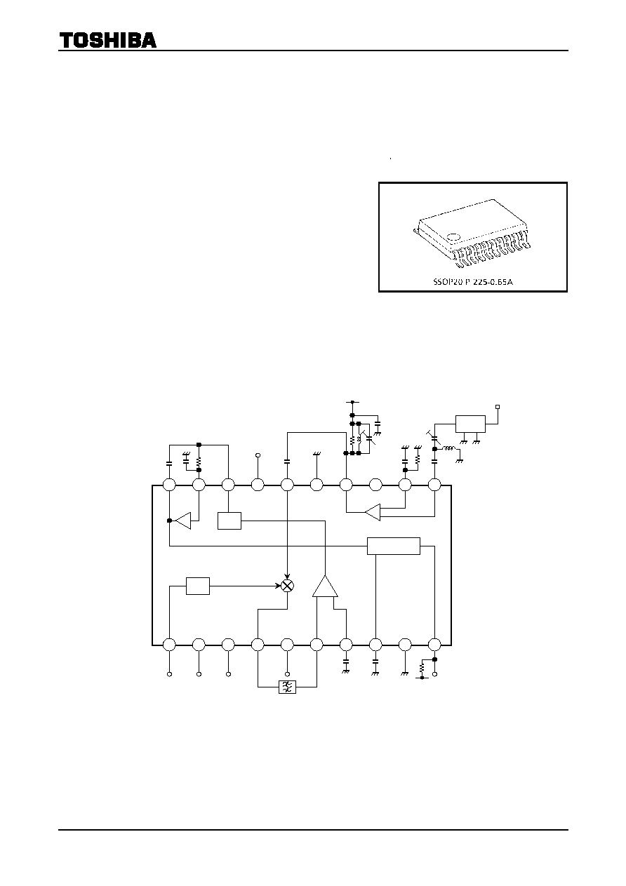
TOSHIBA Bipolar Linear Integrated Circuit Silicon Monolithic
T A 3 1 2 7 3 F N
AM RF/IF Detector IC
The TA31273FN is an RF/IF detector IC for AM radio.
The IC incorporates an RF amp, 2-level comparator, and local x8
circuit.
Features
∑ RF frequency: 240 to 450 MHz
∑ IF frequency: 10.7 MHz
∑ Operating voltage range: 3.0 to 5.5 V
∑ Current dissipation: 6.8 mA (typ.)
(Not operating local oscillator)
∑ Current dissipation at BS: 0 µA (typ.)
∑ Small package: 20-pin SSOP (0.65-mm pitch)
Block Diagram
Weight: 0.09 g (typ.)
10
2
1
3
4
5
6
7
8
9
11
19
20
18
17
16
15
14
13
12
SAW
RSSI
Comparator
◊
8
FIL
IN
FIL
OUT
RSSI BS
MIX
IN
GND1
RF
DEC
MONI
RF
IN
DATA
GND2
REF
IF
DEC
IF
IN
V
CC2
MIX
OUT
LOBS
V
CC1
OSC
IN
RF
OUT

TA31273FN
2002-07-08
2
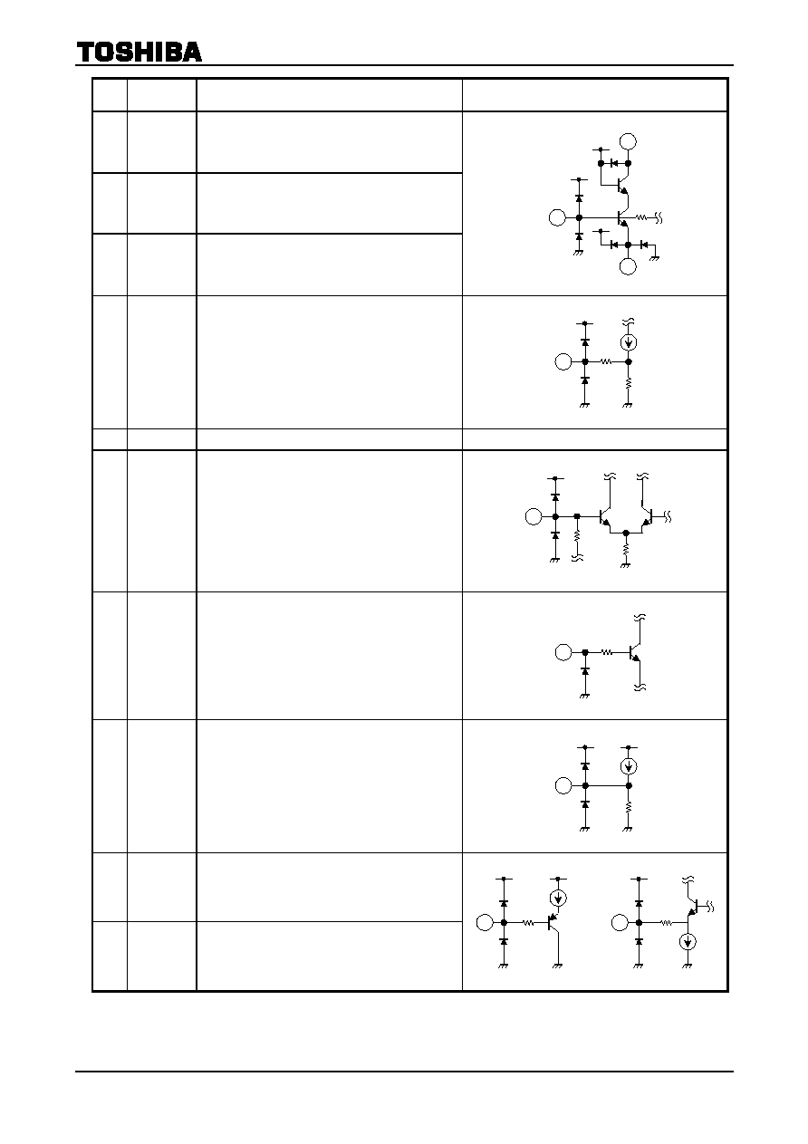
Pin Function
(The Values Of Resistor And Capacitor In The Internal Equivalent Circuit
Are Typical.)
Pin
No.
Pin Name
Function
Internal Equivalent Circuit
1
OSC IN
Local oscillator input pin.
2 V
CC1
Power supply pin 1.
3 LOBS
Lo switch pin.
H: x8 circuit in operation
Lo: Through pass
4
MIX OUT
Mixer output pin.
5 V
CC2
Power supply pin 2.
6
IF IN
IF amp input pin.
7 IF
DEC
IF amp input pin.
Used as a bias coupling pin.
8
REF
AM comparator REF pin.
9
GND2
GND pin 2.
10 DATA
AM waveform shaping output pin.
Open collector output.
Connect a pull-up resistor.
6
7
170
170
3 k
210
4
2 pF
1
15 k
5 k
5 k
15 k
5 k
60 k
3
2 k
10
8
40 k
40 k
COMP
DATA
20
19
500
5.5 k
TA31273FN
2002-07-08
3
Pin
No.
Pin Name
Function
Internal Equivalent Circuit
11 RF IN
RF signal input pin.
12 RF DEC
Emitter pin for internal transistor.
14 RF OUT
RF amp output pin.
13 MONI
Since this pin is connected to an internal circuit, it
should either be left open or connected to GND.
15 GND1
GND pin 1.
16 MIX IN
Mixer input pin.
17 BS
Battery saving pin.
18 RSSI
RSSI output pin.
19 FIL IN
AM LPF input pin.
20 FIL OUT
AM LPF output pin.
Equivalent circuits are given to help understand design of the external circuits to be connected. They do not
accurately represent the internal circuits.
14
12
11
3 k
50 k
17
16
2.4 k
500
18
20 k
20 k
13
20
500
5.5 k
19
TA31273FN
2002-07-08
4
Functions
1. Waveform shaper circuit
(comparator)
The output data (pin 10) are inverted.
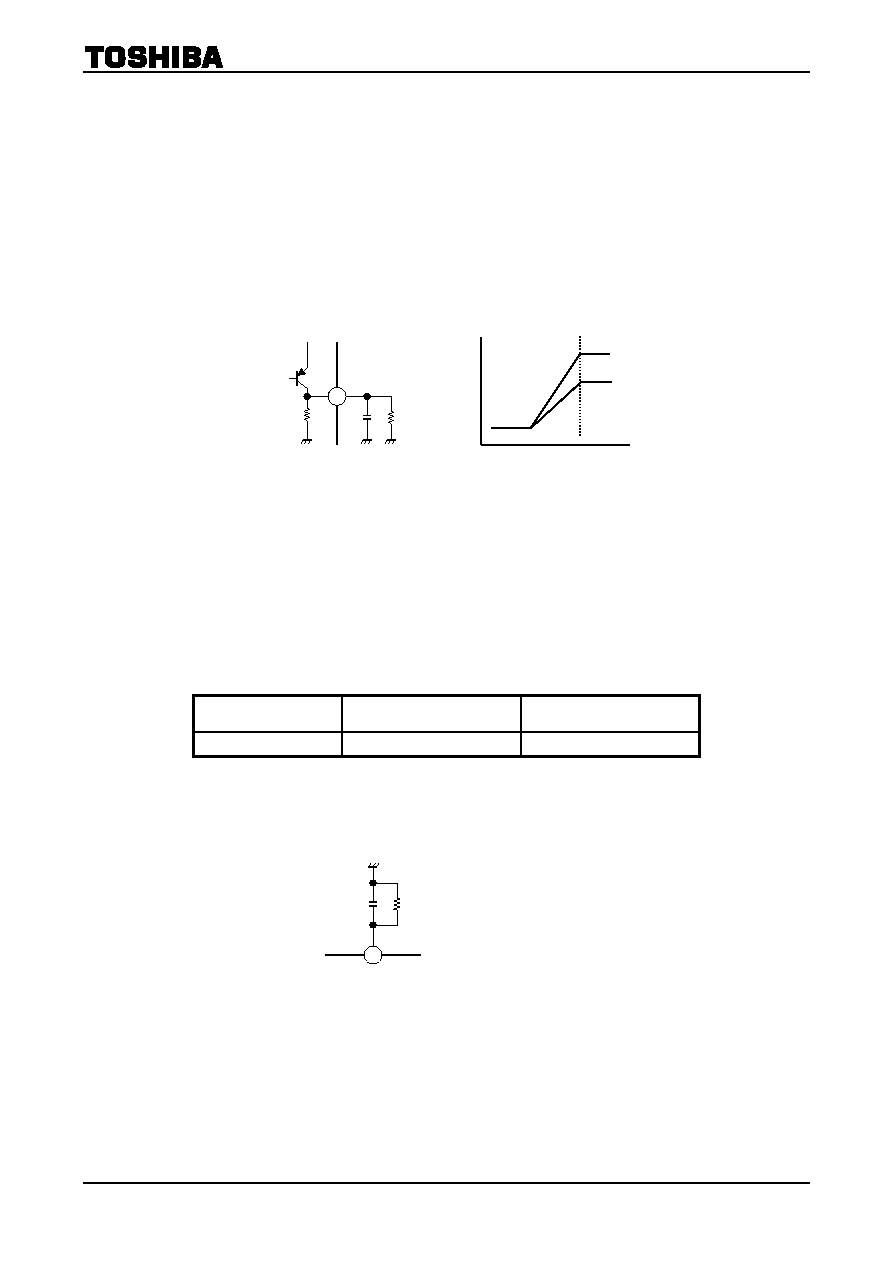
2. RSSI function
DC potential corresponding to the input level of IF IN (pin 6) is output to RSSI (pin 18). Output to RSSI
(pin 18) is converted to a voltage by the internal resistance. Thus, connecting external resistance R to pin
18 varies the gradient of the RSSI output as shown below. Note that due to the displacement of
temperature coefficients between external resistor R and the internal IC resistor, the temperature
characteristic of the RSSI output may change. Also, the maximum RSSI value should be V
CC
- 1 V.
Figure 1 Figure
2
3. V
CC
pin and GND pin
Use the same voltage supply source for V
CC1
(pin 2) and V
CC2
(pin 5) (or connect them). Also, use the same
voltage supply source for GND1 (pin 15) and GND2 (pin 9) (or connect them).
4. Local oscillator circuit
The local oscillator circuit is external-input-only. Input to pin 1 at a level from 95 to 105dB
µV.
By switching the Lo switch (LOBS), the frequency set by the external circuit can be used as-is without
using the x8 circuit.
Lo Switch (LOBS)
H
L
Local oscillation status
x8 circuit in operation
x8 circuit halted/through pass
5. RF amp current adjustment
The RF amp current dissipation can be regulated by varying resistor R as shown in the figure below. When
R
= 1 k, the current dissipation is approximately 800 µA.
Figure
3
12
R
RF DEC
20 k
18
R
IF input level
After R is connected

TA31273FN
2002-07-08
5
6. Battery-saving (BS) function and Lo switch LOBS function
The IC incorporates a battery-saving function and a Lo switch function. These functions offer the following
selection.
BS Pin/LOBS Pin
Circuit Status in the IC
IC Current Dissipation
(at no signal)
H/H
Circuits in operation
∑
x8
circuit
∑
Mixer
∑
RF
amp
∑
Comparator
∑
IF
amp
∑
RSSI
∑ Comparator capacitor charger circuit
6.8 mA (typ.)
H/L
x8 circuit only halted, Frequency set by
external circuit can be used as-is.
3.8 mA (typ.)
L/H
x8 circuit only in operation
3.0 mA (typ.)
L/L
All circuits halted
0 mA (typ.)
7. RF amp gain 1
RF amp gain 1 (G
V
(RF) 1) is a reference value calculated as follows. Measure GRF in the following figure.
Figure 4
G
V
(RF) 1 is calculated as follows:
G
V (RF) 1
= G
RF
- G
V (MIX)
8. IF amp gain
The intended value is 70dB.
9. Waveform-shaping output duty cycle
The specified range of electrical characteristics is only available for single-tone.
10. Local frequency range (after multiplying frequency by 8)
When the multiplier circuit is used, the local frequency will be in the range 250.7 MHz to 439.3 MHz.
27 nH
1000 pF
1 k
4
6
16
14
11
33 nH
SAW
0.01
µ
F
SG
50dB
µ
V
G
RF
6 pF
6 pF

TA31273FN
2002-07-08
6
11. Bit rate filter for AM
The current AM bit rate filter is used as a quadratic filter.
If the filter is to be used at a rate other than 1200 bps, please change the filter constant.
Quadratic filter (NRZ)
(The bit rate filter time constant takes into account the internal resistance RSSI (20 k
).)
R9
R8
C14
C13
1200 bps
47 k
68
k
1500 pF
4700 pF
2400 bps
47 k
68
k
680 pF
2200 pF
4800 bps
47 k
68
k
390 pF
1000 pF
When the filter constants shown below are used, it is not necessary to set the R9 constant value.
R9
R8
C14
C13
1200 bps
20
k
2200 pF
6800 pF
2400 bps
20
k
1500 pF
3300 pF
4800 bps
20
k
820 pF
1800 pF
In addition, the current AM bit rate filter can be used as a tertiary filter.
If the filter is to be used at a rate other than 1200 bps, please change the filter constant.
Quadratic filter (NRZ)
(The bit rate filter time constant takes into account the internal resistance RSSI (20 k
).)
R10
R9
R8
C16
C14
C13
1200 bps
47 k
68
k
68
k
3300 pF
560 pF
0.01
µ
F
2400 bps
47 k
68
k
68
k
1500 pF
270 pF
4700 pF
4800 bps
47 k
68
k
68
k
680 pF
150 pF
2200 pF
When the filter constants shown below are used, it is not necessary to set the R10 constant value.
R10
R9
R8
C16
C14
C13
1200 bps
20
k
20
k
8200 pF
2200 pF
0.033
µ
F
2400 bps
20
k
20
k
3900 pF
1000 pF
0.015
µ
F
4800 bps
20
k
20
k
1800 pF
470 pF
6800 pF
TA31273FN
2002-07-08
7
Maximum Ratings
(Unless Otherwise Specfied Ta = 25∞C, Voltage Value is Determined by
GND (TYP))
Characteristics Symbol
Rating
Unit
Supply voltage
V
CC
6 V
Current dissipation
P
D
710
mW
Operating temperature range
T
opr
-
40~85
∞C
Storage temperature range
T
stg
-
55~150 ∞C
The maximum ratings must not be exceeded at any time. Do not operate the device under conditions outside the above ratings.
Operating available Range
(Unless Otherwise Specified Ta = 25
, Voltage Value is Determined by GND(typ.))
Characteristics Symbol
Test
Circuit
Test Condition
Min
Typ.
Max
Unit
Operating voltage range
V
CC
3.0 5.0 5.5 V
Operating ranges indicate the conditions for which the device is intended to be functional even with the electrical changes.
Electrical Characteristics
(Unless Otherwise Specified : Ta = 25∞C, V
CC
= 5.0V , Rfin = 314.9
MHz, AM = 90%,Ifin = 10.7MHz , af = 600 Hz (square wave))
Characteristics Symbol
Test
Circuit
Test Condition
Min
Typ.
Max
Unit
Current dissipation at no signal
I
ccq
2
V
CC
=
5.0 V, BS/LOBS
="
H/H
"
Fin (LO)
=
40.7 MHz
5.1 6.8 8.5 mA
Current dissipation at battery saving
I
cco
3
0 5
µ
A
RF amp gain 1
G
V (RF) 1
V
in (RF)
=
50dB
µ
V
20
dB
RF amp gain 2
G
V (RF) 2
1
(5) 50
input/output
-
6.5
-
3.5
-
0.5
dB
RF amp input resistance
R
(RF) IN
900
RF amp input capacitance
C
(RF) IN
2.5
pF
RF amp output capacitance
C
(RF) OUT
2
pF
Mixer conversion gain
G
V (MIX)
1
(6)
17.5 21.5 25.5
dB
Mixer input resistance
R
(MIX) IN
1.5
k
Mixer input capacitance
C
(MIX) IN
2.5
dB
Mixer output resistance
R
(MIX) OUT
330
Mixer intercept point
IP3
93
dB
µ
V
IF operating frequency
f
IF
10.7
MHz
IF amp input resistance
R
(IF) IN
330
RSSI output voltage 1
V
RSSI1
1
(1)
V
in (IF)
=
35dB
µ
VEMF
0.1 0.3 0.5 V
RSSI output voltage 2
V
RSSI2
1
(1)
V
in (IF)
=
65dB
µ
VEMF
0.95 1.20 1.45
V
RSSI output voltage 3
V
RSSI3
1
(1)
V
in (IF)
=
100dB
µ
VEMF
1.9 2.3 2.7 V
RSSI output resistance
R
RSSI
15 20 25 k
Waveform shaping output duty cycle
DR
1 (2)
V
in (IF)
=
80dB
µ
VEMF
for single-tone
45 50 55 %
Data output voltage (L level)
V
DATAL
1
(3) I
DATAL
=
1 mA
0.4 V
Data output leakage current (H level)
I
DATAH
1
(4)
2
µ
A
BS pin H-level input voltage
2.7
5.5 V
BS pin L-level input voltage
0
0.2 V
LOBS pin H-level input voltage
2.7
5.5 V
LOBS pin L-level input voltage
0
0.2 V

TA31273FN
2002-07-08
8
Test Circuit
Test Circuit 1
(1) V
RSSI
(2)
D
R
(3) V
DATA L
(4)
I
DATA H
SG
6
18
V
62
0.01
µ
F
1000 pF
SG
6
10
62
0.01
µ
F
100 k
V
CC
V
V
2.5 V
3.0 V
10
V
CC
V
R
=
4.7 k
8
19
10
V
CC
I
=
V/100
◊
10
3
V
100 k
8
V
V
2.5 V
3.0 V
19
10
2
1
3
4
5
6
7
8
9
11
19
20
18
17
16
15
14
13
12
RSSI
COMP
◊
8
FIL
IN
FIL
OUT
RSSI BS
MIX
IN
GND1
RF
DEC
MONI
RF
IN
DATA
GND2
REF
IF
DEC
IF
IN
V
CC2
MIX
OUT
LOBS
V
CC1
OSC
IN
100 k
0.01
µ
F
0.01
µ
F
0.01
µ
F
0.01
µ
F
560 pF
68 k
68 k
3300 pF
47 k
1 k
1000 pF
27nH
1 k
V
CC
V
CC
DATA
R15
C22
C21
C17
C15
V
CC
C13
C14
R8
R9
R10
C16
L4
R13
1000 pF
R14
C24
C25
0.22
µ
F
V
CC
RF
OUT
6 pF
1000 pF
C20
0.01
µ
F
C23
V
CC
V
CC
0.01
µF
BPF
TA31273FN
2002-07-08
9
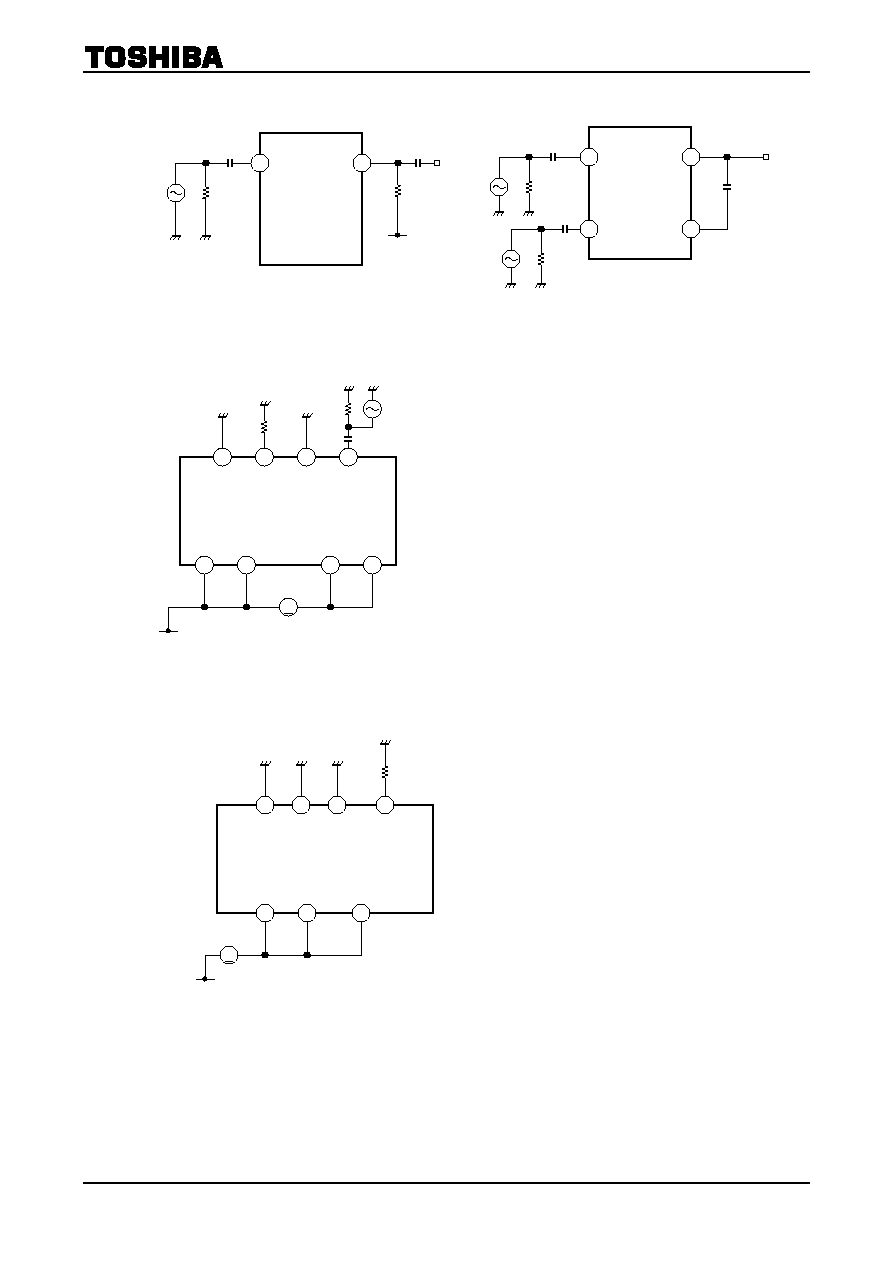
(5) G
v (RF) 2
(6)
G
V (MIX)
Test Circuit 2
I
ccqam
Test Circuit 3
I
cco
SG
11
14
51
1000 pF
51
1000 pF
V
CC
14
5
2
15
12
9
A
17
1 k
SG
1
51
0.01
µ
F
0.01
µ
F
SG
51
16
1000 pF
4
6
14
5
17
2
15
1
1 k
A
12
51 k
0.01
µ
F
SG
9

TA31273FN
2002-07-08
10
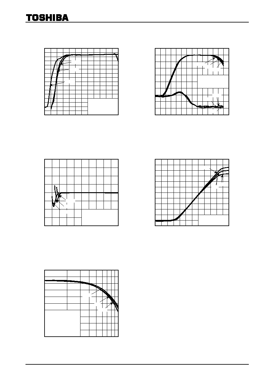
Reference data
This is temperature characteristics data when it used evaluation boards.
This is not guarantee on condition that it is stating except electrical characteristics.
M
i
xer
con
v
er
sion
g
a
in
G
v
(M
i
x
)
(dB
)
Power supply voltage VCC (V)
Current consumption vs.
Power supply voltage characteristics
Curren
t
co
nsum
tion
I ccq
(mA)
Power supply voltage VCC (V)
Current consumption vs.
Power supply voltage characteristics
Curren
t
co
nsum
tion
I ccq
(mA)
Power supply voltage VCC (V)
RF amp gain vs.
Power supply voltage characteristics
RF amp
gain
2
G
v
(
R
F)
2
(d
B)
Power supply voltage VCC (V)
Mixer conversion gain vs.
Power supply voltage characteristics
Power supply voltage VCC (V)
Mixer conversion gain vs.
Power supply voltage characteristics
M
i
xer
con
v
er
sion
g
a
in
G
v
(M
i
x
)
(dB
)
10
0
0 1 2 3 4 5 6
2
4
6
8
25∞C
100∞C
-
40∞C
Fin (Lo)
=
40.7 MHz
Vin (Lo)
=
100 dB
µ
V
BH: H
LOBS: H
0
-
50
1
-
10
-
20
-
30
-
40
2 3 4 5 6
25∞C
100∞C
-
40∞C
Fin (RF)
=
314.9 MHz
Vin (RF)
=
50 dB
µ
V
30
-
30
1
2
3
4
5
6
-
20
-
10
0
10
20
Fin (MIX)
=
314.9 MHz
Vin (MIX)
=
50 dB
µ
V
Fin (Lo)
=
40.7 MHz
Vin (Lo)
=
100 dB
µ
V
LOBS: H
25∞C
110∞C
-
40∞C
30
-
40
1
2
3
4
5
6
-
30
-
20
-
10
0
10
20
-
40∞C
25∞C
110∞C
Fin (MIX)
=
314.9 MHz
Vin (MIX)
=
50 dB
µ
V
Fin (Lo)
=
304.2 MHz
Vin (Lo)
=
100 dB
µ
V
LOBS: L
8
0
0
1
2
3
4
5
6
2
4
6
All internal circuits used
Multiplier circuit turned off
and external circuit used
Only multiplier
circuit used
BS
Fin (Lo)
=
40.7 MHz
Vin (Lo)
=
100 dB
µ
V
Ta
=
25∞C
RSS
I
o
u
tpu
t
vol
t
ag
e
VRSSI
(V)
MIX IN input level Vin (dB
µ
VEMF)
RSSI output voltage characteristics
(MIX input)
3
0
-
20
0
20
40
60
80
120
1
1.5
2
100
2.5
110∞C
25∞C
-
40∞C
Fin (MIX)
=
314.9 MHz
Fin (Lo)
=
40.7 MHz
Vin (Lo)
=
100 dB
µ
V
0.5
TA31273FN
2002-07-08
11
RSS
I
o
u
tpu
t
vol
t
ag
e
VRSSI
(V)
Local input level VLO (dB
µ
V)
Mixer conversion gain vs.
Local input level characteristics
M
i
xer
con
v
er
sion
g
a
in
G
v
(M
i
x
)
(dB
)
IF IN input Vin (IF) (dB
µ
VEMF)
S/N characteristics (IF input)
S
+
N,
N
(dB)
Power supply voltage VCC (V)
FSK duty cycle vs.
Power supply voltage characteristics
FSK du
ty cycle
DR
(
%
)
IF IN input level Vin (dB
µ
VEMF)
RSSI output voltage characteristics
(IF input)
Input frequency Fin (MIX) (MHz)
Mixer conversion gain frequency
characteristics
M
i
xer
con
v
er
sion
g
a
in
G
v
(M
IX)
(d
B)
25
0
100
5
10
15
20
1000
VCC
=
5 V
Vin (MIX)
=
50 dB
µ
V
Vin (Lo)
=
100 dB
µ
V
LOBS
=
"L"
*
Terminate the IF input
impedance.
110∞C
25∞C
-
40∞C
Fin (MIX)
=
314.9 MHz
Vin (MIX)
=
50 dB
µ
V
Fin (Lo)
=
40.7 MHz
25
-
15
60 70 80 90 100 110 120
-
5
5
15
-
10
0
10
20
110∞C
25∞C
-
40∞C
10
-
9
-
10 10 30 50 70 90
130
-
7
-
3
-
5
0
110
-
40∞C
25∞C
110∞C
-
40∞C
110∞C
25∞C
Fin (IF)
=
10.7 MHz
AM
=
90%
Fmod
=
600 Hz
60.0
40.0
1.00 2.00 3.00 4.00 5.00 6.00
50.0
45.0
55.0
-
40∞C
25∞C
110∞C
Fin (IF)
=
10.7 MHz
Vin (IF)
=
50 dB
µ
VEMF
AM
=
90%
Fmod
=
600 Hz
3.0
40.0
0 20 40 60 80
120
1.0
2.5
2.0
1.5
0.5
100
-
40∞C
25∞C
110∞C
Fin (IF)
=
10.7 MHz

TA31273FN
2002-07-08
12
Application Circuit
X1 TR-1Tokyo Denpa Co., Ltd.
BPFSFE10.7MA5-AMurata Manufacturing Co., Ltd.
SAWSAFCH315MSM0T00B0SMurata Manufacturing Co., Ltd.
10
2
1
3
4
5
6
7
8
9
11
19
20
18
17
16
15
14
13
12
SAW
RSSI
Comparator
◊
8
FIL
IN
FIL
OUT
RSSI BS MIX
IN
GND1
RF
DEC
MONI
RF
IN
DATA
GND2
REF
IF
DEC
IF
IN
V
CC2
MIX
OUT
LOBS
V
CC1
OSC
IN
100 k
0.01
µ
F
0.01
µ
F
40.7 MHz
0.01
µ
F
1 pF
120 k
3.3 k
0.01
µ
F
33 k
0.01
µ
F
560 pF
68 k
68 k
3300 pF
47 k
1 k
33 nH
1000 pF
27nH
1 k
V
CC
BPF
V
CC
DATA
R15
C22
C21
C17
C15
V
CC
10
µ
F
56 pF
C7
C9
R2
47 pF
C3
R3
C2
C8
C13
C14
R8
R9
R10
C16
L4
R13
1000 pF
R14
C24
C25
6 pF
RF IN
0.22
µ
F
V
CC
RF
OUT
6 pF
1000 pF
C20
0.01
µ
F
C23
R4
V
CC
V
CC
X1
TA31273FN
2002-07-08
13
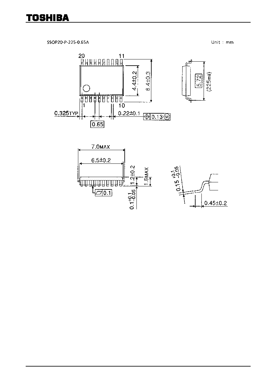
Package Dimensions
Weight: 0.09 g (typ.)

TA31273FN
2002-07-08
14
∑
TOSHIBA is continually working to improve the quality and reliability of its products. Nevertheless, semiconductor
devices in general can malfunction or fail due to their inherent electrical sensitivity and vulnerability to physical
stress. It is the responsibility of the buyer, when utilizing TOSHIBA products, to comply with the standards of
safety in making a safe design for the entire system, and to avoid situations in which a malfunction or failure of
such TOSHIBA products could cause loss of human life, bodily injury or damage to property.
In developing your designs, please ensure that TOSHIBA products are used within specified operating ranges as
set forth in the most recent TOSHIBA products specifications. Also, please keep in mind the precautions and
conditions set forth in the "Handling Guide for Semiconductor Devices," or "TOSHIBA Semiconductor Reliability
Handbook" etc..
∑
The TOSHIBA products listed in this document are intended for usage in general electronics applications
(computer, personal equipment, office equipment, measuring equipment, industrial robotics, domestic appliances,
etc.). These TOSHIBA products are neither intended nor warranted for usage in equipment that requires
extraordinarily high quality and/or reliability or a malfunction or failure of which may cause loss of human life or
bodily injury ("Unintended Usage"). Unintended Usage include atomic energy control instruments, airplane or
spaceship instruments, transportation instruments, traffic signal instruments, combustion control instruments,
medical instruments, all types of safety devices, etc.. Unintended Usage of TOSHIBA products listed in this
document shall be made at the customer's own risk.
∑
The products described in this document are subject to the foreign exchange and foreign trade laws.
∑
The information contained herein is presented only as a guide for the applications of our products. No
responsibility is assumed by TOSHIBA CORPORATION for any infringements of intellectual property or other
rights of the third parties which may result from its use. No license is granted by implication or otherwise under
any intellectual property or other rights of TOSHIBA CORPORATION or others.
∑
The information contained herein is subject to change without notice.
000707EBA
RESTRICTIONS ON PRODUCT USE