 | –≠–ª–µ–∫—Ç—Ä–æ–Ω–Ω—ã–π –∫–æ–º–ø–æ–Ω–µ–Ω—Ç: TLP561J | –°–∫–∞—á–∞—Ç—å:  PDF PDF  ZIP ZIP |
TLP561J
2002-09-25
1
TOSHIBA Photocoupler GaAs IRed & Photo-Triac
TLP561J
Triac Driver
Programmable Controllers
AC-Output Module
Solid State Relay
The TOSHIBA TLP561J consists
of a zero voltage crossing turn-on
photo-triac optically coupled to a gallium arsenide infrared emitting diode in a six
lead plastic DIP package.
∑ Peak off-state voltage: 600V(min.)
∑ On-state current: 100mA(max.)
∑ Isolation voltage: 2500V
rms
(min.)
∑ UL recognized: UL1577, file no. E67349
∑ Isolation operating voltage: 2500V
ac
or
300V
dc
for isolation
Groupe C
*1
∑ Trigger LED current
*Ex. (IFT7); TLP561J(IFT7)
(Note ): Application type name for certification test, please
use standard product type name, i.e.
TLP561J(IFT7):
TLP561J
*1: According to VDE0110, table 4.
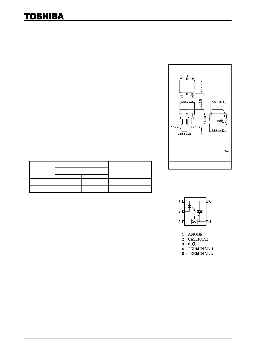
Pin Configuration (top view)
Unit in mm
TOSHIBA 11
-7A9
Weight: 0.39g
Trigger LED Current (mA)
V
T
=6V, Ta=25∞C
Classi
-
Fication*
Min. Max.
Marking Of
Classification
(IFT7)
7
T7
Standard
10
T7,
blank
TLP561J
2002-09-25
2
Maximum Ratings
(Ta = 25∞C)
Characteristic Symbol
Rating
Unit
Forward current
I
F
50
mA
Forward current derating (Ta 53∞C)
I
F
/ ∞C
-0.7
mA / ∞C
Peak forward current (100µs pulse, 100pps)
I
FP
1
A
Reverse voltage
V
R
5
V
LE
D
Junction temperature
T
j
125
∞C
Off
-state output terminal voltage
V
DRM
600 V
Ta = 25∞C
100
On
-state RMS current
Ta = 70∞C
I
T(RMS)
50
mA
On
-state current derating (Ta 25∞C)
I
T
/ ∞C
-1.1
mA / ∞C
Peak on
-state current (100µs pulse, 120pps)
I
TP
2
A
Peak nonrepetitive surge current
(Pw = 10ms, DC = 10%)
I
TSM
1.2 A
Det
e
c
t
or
Junction temperature
T
j
115
∞C
Storage temperature range
T
stg
-55~125 ∞C
Operating temperature range
T
opr
-40~100 ∞C
Lead soldering temperature (10s)
T
sol
260
∞C
Isolation voltage (AC, 1min., R.H. 60%)
BV
S
2500
V
rms
Recommended Operating Conditions
Characteristic Symbol
Min.
Typ.
Max.
Unit
Supply voltage
V
AC
240
V
ac
Forward current
I
F
15
20
25
mA
Peak on
-state current
I
TP
A
Operating temperature
T
opr
-25
85 ∞C
TLP561J
2002-09-25
3
Individual Electrical Characteristics
(Ta = 25∞C)
Characteristic Symbol
Test
Condition
Min.
Typ.
Max.
Unit
Forward voltage
V
F
I
F
=
10mA
1.0 1.15 1.3 V
Reverse current
I
R
V
R
= 5 V
10 µA
LE
D
Capacitance C
T
V = 0, f = 1MHz
30 pF
Peak off
-state current
I
DRM
V
DRM
= 600V
10
1000
nA
Peak on
-state voltage
V
TM
I
TM
= 100mA
1.7
3.0 V
Holding current
I
H
0.6
mA
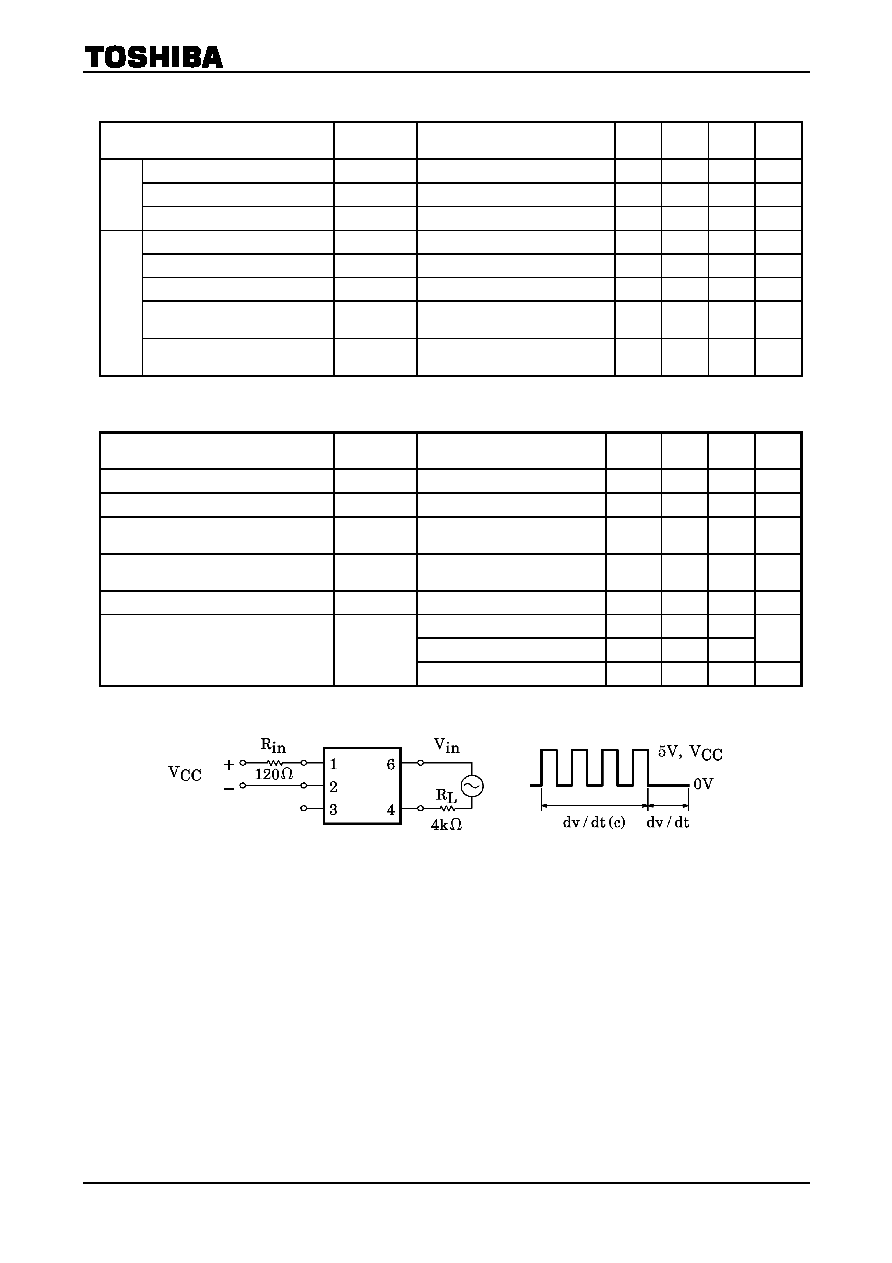
Critical rate of rise of
off
-state voltage
dv / dt
V
in
= 240V
rms,
Ta = 85∞C
(Fig.1)
200 500 V
/
µs
Det
e
c
t
or
Critical rate of rise of
commutating voltage
dv / dt(c)
V
in
= 60V
rms
, I
T
= 15mA
(Fig.1)
0.2 V
/
µs
Coupled Electrical Characteristics
(Ta = 25∞C)
Characteristics Symbol
Test
Condition
Min.
Typ.
Max.
Unit
Trigger LED current
I
FT
V
T
= 6V, R
L
= 100
5 10
mA
Inhibit voltage
V
IH
I
F
= Rated I
FT
50 V
Leakage in inhibited state
I
IH
I
F
= Rated I
FT
V
T
= Rated V
DRM
200
600
µA
Capacitance
(input to output)
C
S
V
S
= 0, f = 1MHz
0.8 pF
Isolation resistance
R
S
V
S
= 500V
5◊10
10
10
14
AC, 1 minute
2500
AC, 1 second, in oil
5000
V
rms
Isolation voltage
BV
S
DC, 1 minute, in oil
5000
V
dc
Fig.1: dv / dt test circuit
TLP561J
2002-09-25
4

TLP561J
2002-09-25
5