TOSHIBA
TOSHIBA CORPORATION
1
TLCS-900 Series
TMP93CM40/TMP93CM41
The information contained here is subject to change without notice.
The information contained herein is presented only as guide for the applications of our products. No responsibility is assumed by TOSHIBA for any infringements of patents or other rights of the third parties
which may result from its use. No license is granted by implication or otherwise under any patent or patent rights of TOSHIBA or others. These TOSHIBA products are intended for usage in general electronic
equipments (office equipment, communication equipment, measuring equipment, domestic electrification, etc.) Please make sure that you consult with us before you use these TOSHIBA products in equip-
ments which require high quality and/or reliability, and in equipments which could have major impact to the welfare of human life (atomic energy control, spaceship, traffic signal, combustion control, all types
of safety devices, etc.). TOSHIBA cannot accept liability to any damage which may occur in case these TOSHIBA products were used in the mentioned equipments without prior consultation with TOSHIBA.
Low Voltage/Low Power
CMOS 16-bit Microcontrollers
TMP93CM40F/TMP93CM41F
1.
Outline and Device Characteristics
TMP93CM40/M41 are high-speed advanced 16-bit microcon-
trollers developed for controlling medium to large-scale equip-
ment. The TMP93CM41 does not have a ROM, the
TMP96CM40 has a built-in ROM. Otherwise, the devices func-
tion in the same way.
TMP93CM40F/TMP93CM41F are housed in 100-pin
mini flat package. Device characteristics are as follows:
(1) Original 16-bit CPU (900L CPU)
� TLCS-90 instruction mnemonic upward compatible.
� 16M-byte linear address space
� General-purpose registers and register bank system
� 16-bit multiplication/division and bit transfer/arithmetic
instructions
� High-speed micro DMA
- 4 channels (1.6
�
s/2 bytes at 20MHz)
(2) Minimum instruction execution time
- 200ns at 20MHz
(3) Internal RAM: 2K byte
Internal ROM:
(4) External memory expansion
� Can be expanded up to 16M bytes (for both programs and
data).
� AM8/16 pin (select the external data bus width).
� Can mix 8- and 16-bit external data buses.
...
Dynamic data bus sizing
(5)
8-bit timer: 2 channels
(6)
8-bit PWM timer: 2 channels
(7) 16-bit timer: 2 channels
(8) Pattern generator: 4 bits, 2 channels
(9) Serial interface: 2 channels
(10) 10-bit A/D converter: 4 channels
(11) Watchdog timer
(12) Chip select/wait controller: 3 blocks
(13) Interrupt functions
� 2 CPU interrupts
...
...
SWI instruction, and Illegal instruction
� 14 internal interrupts
� 6 external interrupts
(14) I/O ports:
79 pins for TMP93CM40 and 61 pins for TMP93CM41
(15) Standby function : 4 halt modes (RUN, IDLE2, IDLE1,
STOP)
(16) Clock Gear Function
� High-frequency clock can be changed fc to fc/16
� Dual clock operation
(17) Wide Operating Voltage
� V
CC
= 2.7 to 5.5V
TMP93CM40
32K-byte ROM
TMP93CM41
None
7-level priority can be set.

2
TOSHIBA CORPORATION
TMP93CM40/TMP93CM41
Figure 1. TMP93CM40/TMP93CM41 Block Diagram
TOSHIBA CORPORATION
3
TMP93CM40/TMP93CM41
2.
Pin Assignment and Functions
The assignment of input/output pins for TMP93CM40/
TMP93CM41, their name and outline functions are described
below.
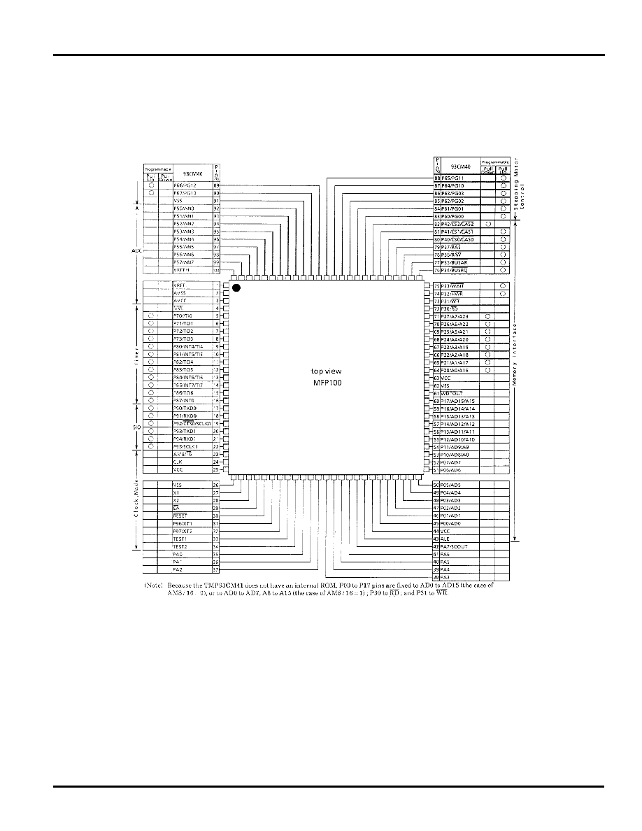
Figure 2.1. Pin Assignment (100-pin MFP)
2.1 Pin Assignment
Figure 2.1 shows pin assignment of TMP93CM40F/
TMP93CM41F.

4
TOSHIBA CORPORATION
TMP93CM40/TMP93CM41
2.2 Pin Names and Functions
The names of input/output pins and their functions are described below.
Note:
With the external DMA controller, this device's built-in memory or built-in I/O cannot be accessed using the BUSRQ and BUSAK pins.
Table 2.2. Pin Names and Functions
Pin Name
Number
of Pins
I/O
Functions
P00 to P07
AD0 to AD7
8
I/O
Tri-state
Port 0: I/O port that allows I/O to be selected on a bit basis
Address / data (lower): 0 to 7 for address / data bus
P10 to P17
AD8 to AD15
A8 to A15
8
I/O
Tri-state
Output
Port 1: I/O port that allows I/O to be selected on a bit basis
Address data (upper): 8 to 15 for address / data bus
Address: 8 to 15 for address bus
P20 to P27
A0 to A7
A16 to A23
8
I/O
Output
Output
Port 2: I/O port that allows selection of I/O on a bit basis (with pull-down resistor)
Address: 0 to 7 for address bus
Address: 16 to 23 for address bus
P30
RD
1
Output
Output
Port 30: Output port
Read: Strobe signal for reading external memory
P31
WR
1
Output
Output
Port 31: Output port
Write: Strobe signal for writing data on pins AD0 to7
P32
HWR
1
I/O
Output
Port 32: I/O port (with pull-up resistor)
High write: Strobe signal for writing data on pins AD8 to 15
P33
WAIT
1
I/O
Input
Port 33: I/O port (with pull-up resistor)
Wait: Pin used to request CPU bus wait
P34
BUSRQ
1
I/O
Input
Port 34: I/O port (with pull-up resistor)
Bus request: Signal used to request high impedance for AD0 to 15, A0 to 23, RD, WR, HWR, R/W, RAS, CS0,
CS1, and CS2 pins. (For external DMAC)
P35
BUSAK
1
I/O
Output
Port 35: I/O (with pull-up resistor)
Bus acknowledge: Signal indicating that AD0 to 15, A0 to 23, RD, WR, HWR, R/W, RAS, CS0, CS1, and CS2
pins are at high impedance after receiving BUSRQ. (For external DMAC)
P36
R/W
1
I/O
Output
Port 36: I/O port (with pull-up resistor)
Read/write: 1 represents read or dummy cycle; 0, write cycle.
P37
RAS
1
I/O
Output
Port 37: I/O port (with pull-up resistor)
Row address strobe: Outputs RAS strobe for DRAM.
P40
CS0
CAS0
1
I/O
Output
Output
Port 40: I/O port (with pull-up resistor)
Chip select 0: Outputs 0 when address is within specified address area.
Column address strobe 0: Outputs CAS strobe for DRAM when address is within specified address area.

TOSHIBA CORPORATION
5
TMP93CM40/TMP93CM41
Pin Name
Number
of Pins
I/O
Functions
P41
CS1
CAS1
1
I/O
Output
Output
Port 41: I/O port (with pull-up resistor)
Chip select 1: Outputs 0 if address is within specified address area.
Column address strobe 1: Outputs CAS strobe for DRAM if address is within specified address area.
P42
CS2
CAS2
1
I/O
Output
Output
Port 42: I/O port (with pull-up resistor)
Chip select 2: Outputs 0 if address is within specified address area.
Column address strobe 2: Outputs CAS strobe for DRAM if address is within specified address area.
P50 to P53
AN0 to AN3
4
Input
Input
Port 5: Input port
Analog input: Input to A/D converter
VREF
1
Input
Pin for reference voltage input to A/D converter
AGND
1
Input
Ground pin for A/D converter
P60 to P63
PG00 to PG03
4
I/O
Output
Ports 60 to 63: I/O ports that allow selection of I/O on a bit basis (with pull-up resistor)
Pattern generator ports: 00 to 03
P64 to P67
PG10 to PG13
4
I/O
Output
Ports 64 to 67: I/O ports that allow selection of I/O on a bit basis (with pull-up resistor)
Pattern generator ports: 10 to 13
P70
TI0
1
I/O
Input
Port 70: I/O port (with pull-up resistor)
Timer input 0: Timer 0 input
P71
T01
1
I/O
Output
Port 71: I/O port (with pull-up resistor)
Timer output 1: Timer 0 or 1 output
P72
T02
1
I/O
Output
Port 72: I/O port (with pull-up resistor)
PWM output 2: 8-bit PWM timer 2 output
P73
T03
1
I/O
Output
Port 73: I/O port (with pull-up resistor)
PWM output 3: 8-bit PWM timer 3 output
P80
TI4
INT4
1
I/O
Input
Input
Port 80: I/O port (with pull-up resistor)
Timer input 4: Timer 4 count/capture trigger signal input
Interrupt request pin 4: Interrupt request pin with programmable rising/falling edge
P81
TI5
INT5
1
I/O
Input
Input
Port 81: I/O port (with pull-up resistor)
Timer input 5: Timer 4 count/capture trigger signal input
Interrupt request pin 5: Interrupt request pin with rising edge
P82
TO4
1
I/O
Output
Port 82: I/O port (with pull-up resistor)
Timer output 4: Timer 4 output pin
P83
TO5
1
I/O
Output
Port 83: I/O port (with pull-up resistor)
Timer output 5: Timer 4 output pin