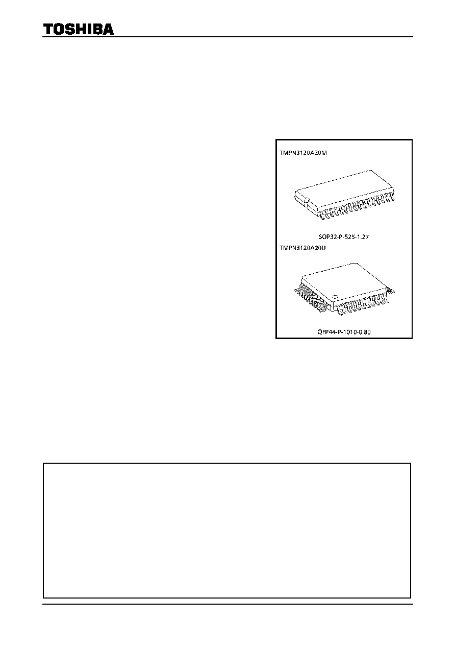
TMPN3120A20M/U
2003-07-01 1/12
TOSHIBA CMOS DIGITAL INTEGRATED CIRCUIT SILICON MONOLITHIC
TMPN3120A20M, TMPN3120A20U
Neuron
Æ
Chip
For Distributed Intelligent Control Networks (L
ON
W
ORKS
Æ
)
The Neuron Chip (TMPN3120A20M and TMPN3120A20U) provides
double the performance of previous Neuron Chips. It supports a
response time of 3 to 4 ms across a L
ON
W
ORKS
Network and has
double the input / output (I / O) performance of the previous Neuron
Chip in terms of both response time and data transmission speed.
Neuron Chips have all the built-in communications and control
functions required to implement L
ON
W
ORKS
nodes. These nodes
may then be easily integrated into highly-reliable distributed
intelligent control networks.
The typical functions for this chip are explained below.
FEATURES
New features
( In comparison with TMPN3120FE3M and TMPN3120A20M /U )
∑ Enhanced communication port
∑ The package is QFP44-P-1010-0.80 (TMPN3120A20U only)
Weight
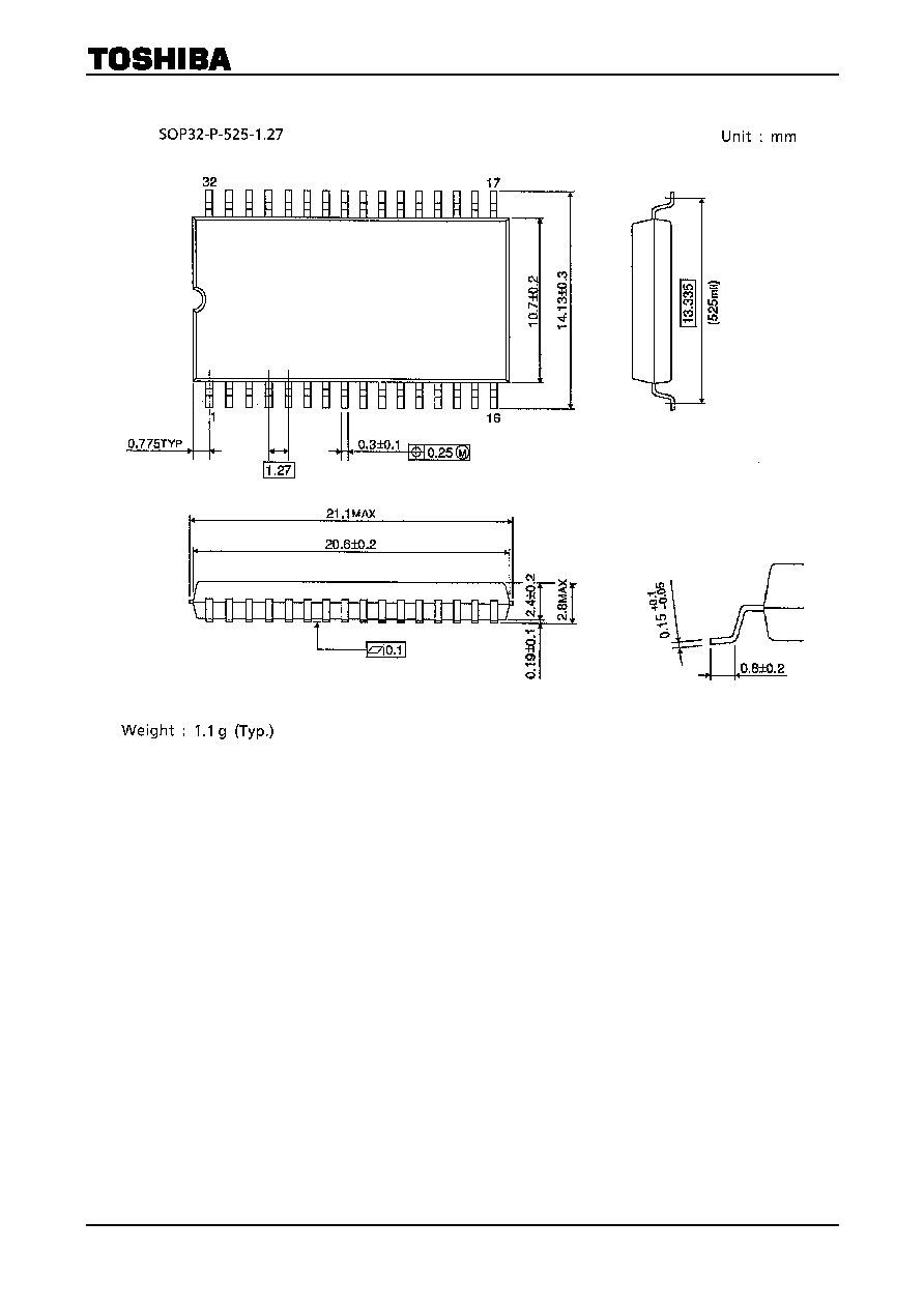
SOP32-P-525-1.27 : 1.1g (Typ.)
QFP44-P-1010-0.80 : 0.6g (Typ.)
∑ TOSHIBA is continually working to improve the quality and reliability of its products. Nevertheless, semiconductor devices in general
can malfunction or fail due to their inherent electrical sensitivity and vulnerability to physical stress. It is the responsibility of the
buyer, when utilizing TOSHIBA products, to comply with the standards of safety in making a safe design for the entire system, and
to avoid situations in which a malfunction or failure of such TOSHIBA products could cause loss of human life, bodily injury or
damage to property.
In developing your designs, please ensure that TOSHIBA products are used within specified operating ranges as set forth in the
most recent TOSHIBA products specifications. Also, please keep in mind the precautions and conditions set forth in the "Handling
Guide for Semiconductor Devices," or "TOSHIBA Semiconductor Reliability Handbook" etc..
∑ The TOSHIBA products listed in this document are intended for usage in general electronics applications (computer, personal
equipment, office equipment, measuring equipment, industrial robotics, domestic appliances, etc.). These TOSHIBA products are
neither intended nor warranted for usage in equipment that requires extraordinarily high quality and/or reliability or a malfunction or
failure of which may cause loss of human life or bodily injury ("Unintended Usage"). Unintended Usage include atomic energy
control instruments, airplane or spaceship instruments, transportation instruments, traffic signal instruments, combustion control
instruments, medical instruments, all types of safety devices, etc.. Unintended Usage of TOSHIBA products listed in this document
shall be made at the customer's own risk.
∑ The products described in this document are subject to the foreign exchange and foreign trade laws.
∑ The information contained herein is presented only as a guide for the applications of our products. No responsibility is assumed by
TOSHIBA CORPORATION for any infringements of intellectual property or other rights of the third parties which may result from its
use. No license is granted by implication or otherwise under any intellectual property or other rights of TOSHIBA CORPORATION or
others.
∑ The information contained herein is subject to change without notice.
000707EBA1

TMPN3120A20M/U
2003-07-01 2/12
Main features of the 20MHz Neuron Chip
(In comparison with the TMPN3120E1M and TMPN3120A20M / U)
∑ Increased communication speed
The maximum transmission speed has been increased two-fold.
1.25 Mbps 2.5 Mbps (*1)
*1: This value applies to Single-Ended Mode only.
∑ Shortened response time
The amount of time required from I / O input to I / O output has been greatly reduced.
Maximum speed 7ms 3~4 ms
∑ Increased IO object speed
The execution time for all objects has been halved.
Example) Serial I / O 9600bps
Parallel I / O 1.2µs / byte
∑ Development tool support
The current LonBuilder
Æ
and NodeBuilder
Æ
development tools can be used to develop applications for the
TMPN3120A20M and TMPN3120A20U (L.B ver. 3.0 or 3.01 is needed). Updated symbol table files for
the Neuron Chip firmware are available from Echelon. If your application requires a 20MHz input clock,
a utility program available from Echelon may be used to convert the programmer files.
* The conversion utilities can be obtained from the Echelon Web Site at http://www.echelon.com.
I / O Functions
∑ Eleven programmable I / O pins.
∑ Two programmable 16-bit timers and counters built in.
∑ 34 different types of I / O functions to handle a wide range of input and output.
∑ ROM firmware image containing pre-programmed I / O drivers, greatly simplifying application programs.
Network functions
∑ Two CPUs for communication protocol processing built in.
The communications and application CPUs execute in parallel.
∑ Equipped with a built-in LonTalk protocol which supports all seven levels of the OSI reference model with
ISO.
∑ The ROM firmware image contains a complete network operating system, greatly simplifying application
programs.
∑ Built-in twisted-pair wire transceiver with improved common mode and drive current capabilities.
∑ Equipped with communications modes and communication speeds which support various types of external
transceivers.
Supports twisted-pair wire, power line, radio ( RF ), infrared, coaxial cables, and fiber optics.
∑ Communication port transceiver modes and logical addresses stored within the EEPROM.
Can be amended via the network.
TMPN3120A20M/U
2003-07-01 3/12
Other functions
∑ Application programs are also stored within the EEPROM.
Can be updated by downloading over the network.
∑ Built-in watch-dog timer.
∑ Each chip has a unique ID number.
Effective during the logical installation of networks.
∑ Low electrical consumption mode supported with a sleep mode.
∑ Built in Selectable Reset time
Prolongs the power-ON reset time for at least 50ms and keeps the operation stable during that time. The
reset time can be selected 50ms delay mode or 3clock delay mode by program after the device is in power-ON.
∑ High-impedance communication port ( CP0 to CP3 )
The Communication port pins ( CP0 to CP3 ) attain high impedance. This eliminates the need for an external
relay.
∑ Built-in low-voltage detection circuit.
Prevents in correct operations and writing errors in the EEPROM during drops in power voltage.
An external LVD must be used to assert reset at power supply voltage below 4.5 V if Neuron Chip is operated
at 20 MHz.
∑ Programmable LVD (Low Voltage Detection) circuit.
LVDin pin is prepared in order to make it reset on arbitrary voltage.
∑ Firmware version 9.
Timing for the main I / O objects during 20 MHz Neuron Chip operations
I / O MODEL
10 MHz TIMING
20 MHz TIMING
Parallel
2.4µs / byte
1.2µs / byte
Bitshift
1, 10 or 15 kbps
2, 20 or 30 kbps
Magcard
Up to 8334 bps
Up to 16668 bps
Magtrack1
Up to 7246 bps
Up to 14492 bps
Neurowire Master
1, 10 or 20 kbps
2, 20 or 40 kbps
Neurowire Slave
Up to 18 kbps
Up to 36 kbps
Serial
600, 1200, 2400 or 4800 bps
1200, 2400, 4800 or 9600 bps
Touch Supported
Not
supported
Frequency Output
Resolution0.4 to 51.2µs
Max Range 26.21 to 3355 ms
Resolution0.2 to 25.6µs
Max Range 13.1 to 1678 ms
Other Timer / Counter
Resolution0.2 to 25.6µs
Max Range 13.1 to 1678 ms
Resolution0.1 to 12.8µs
Max Range 6.55 to 839 ms
The specifications for the main timers during 20 MHz
operations are as follows :
Watchdog Timer
420 ms
Millisecond Timers
1 to 32000 ms
Second Timers
1 to 65000 s
Delay ( ) Function
1 to 32767 counts
Get_Tick_Count ( )
Function
409.6µs per count

TMPN3120A20M/U
2003-07-01 4/12
BLOCK DIAGRAM
ITEM TMPN3120A20M
TMPN3120A20U
CPU
8-bit CPU ◊ 3
8-bit CPU◊ 3
RAM
1,024 bytes
1,024 bytes
ROM
16,384 bytes
16,384 bytes
EEPROM
1,024 bytes
1,024 bytes
16-bit Timer / Counter
2 channels
2 channels
External Memory Interface
No
No
Package
32-pin SOP
44-pin QFP

TMPN3120A20M/U
2003-07-01 5/12
PIN CONNECTION
* : All NC pins should be open.

TMPN3120A20M/U
2003-07-01 6/12
PIN FUNCTION
PIN No.
TMPN3120A20M TMPN3120A20U
PIN NAME
I / O
PIN FUNCTION
15
15
CLK1
Input
Oscillator connection, or external clock input.
14 14
CLK2
Output
Oscillator connection. Leave open when external
clock is input to CLK1.
1 40
~RESET
I / O
(built-in pull-up)
Reset pin. ( Active low )
8 5
~SERVICE
I / O
(built-in
configurable
pull-up)
Service pin. Indicator output during operation.
7~4 4~2,
43
IO
0
~IO
3
I / O
Large current sink capacity ( 20 mA ).
General I / O port.
3, 30~28
42, 36, 35, 32
IO
4
~IO
7
I / O
(built-in
configurable
pull-up)
General I / O port. One of IO
4
to IO
7
can be
specified as No.1 timer / counter input. Output
signal can be output to IO
0
.
IO
4
can be used as the No.2 timer / counter input
with IO
1
as output.
27, 26, 24
31, 30, 27
IO
8
~IO
10
I / O
General I / O port. Can be used for serial
communication with other device.
11, 12, 18, 25, 32
9, 10, 19, 29, 38
V
DD
Input
Power input ( 5.0 V Typ. )
9, 10, 13, 16, 23, 31
7, 8, 13, 16, 26, 37
V
SS
Input
Power input ( 0 V GND )
2 41
LVD
in
Input
Input pin for programmable LVD
( Normally connect to V
DD
)
19, 20, 17, 21, 22
20, 21, 18, 24, 25
CP
0
~CP
4
I / O
Bidirectional port for communications. Supports
several communications protocols by specifying
mode.
1, 6, 11, 12, 17, 22,
23, 28, 33, 34, 39,
44
NC
Do not connect anything. Leave pins open.
* : The ~SERVICE and IO
4
to IO
7
terminals are programmable pull-ups.
All V
DD
terminals must be externally connected.
All V
SS
terminals must be externally connected.
TMPN3120A20M/U
2003-07-01 7/12
MAXIMUM RATINGS
( V
SS
= 0V, V
SS
typ.)
ITEM SYMBOL
RATING
UNIT
Power Supply Voltage
V
DD
-0.3~7.0 V
Input Voltage
V
IN
-0.3 to V
DD
+ 0.3 V
V
Input Voltage CP
0
-CP
3
V
IN
(2)
-0.5 to V
DD
+ 1.3 V
V
IN
(2)
< 7.3
V
Power Dissipation
P
D
800 mW
Storage Temperature
T
stg
-65~150 ∞C
OPERATING CONDITIONS
ITEM SYMBOL
MIN TYP.
MAX UNIT
Operating Voltage
V
DD
4.5 5.0 5.5 V
V
IH
2.0
V
DD
V
Input Voltage ( TTL )
V
IL
V
SS
0.8 V
V
IH
V
DD
- 0.8 V
V
DD
V
Input Voltage ( CMOS )
V
IL
V
SS
0.8 V
V
IH
V
DD
+ 1.0 V
Input Voltage CP
0
-CP
3
( differential mode )
V
IL
-0.1
V
Operating Frequency
f
osc
0.625
20
MHz
Operating Temperature
T
opr
-40
85 ∞C
TMPN3120A20M/U
2003-07-01 8/12
ELECTRICAL CHARACTERISTICS
DC characteristic
( V
DD
= 5.0 V ± 10%, V
SS
= 0 V, Ta = -40~85∞C )
( Above operating conditions apply unless otherwise states. )
ITEM
SYMBOL
PINS
TEST CONDITION
MIN
MAX
UNIT
LOW Level Input Voltage (1)
V
IL
(1)
IO
0
~IO
10
CP
0
, CP
3
, CP
4
,
~SERVICE
0
0.8
V
LOW Level Input Voltage (2)
V
IL
(2)
~RESET
0
V
DD
◊ 0.3
V
HIGH Level Input Voltage (1)
V
IH
(1)
IO
0
~IO
10
CP
0
, CP
3
, CP
4
,
~SERVICE
2.0
V
DD
V
HIGH Level Input Voltage (2)
V
IH
(2)
~RESET
V
DD
- 0.7 V
V
DD
V
I
OL
= 20mA
0
0.8
LOW Output Voltage (1)
V
OL
(1)
IO
0
~IO
3
~SERVICE,
~RESET
I
OL
= 10mA
0
0.4
V
LOW Output Voltage (2)
V
OL
(2)
CP
2
, CP
3
I
OL
= 40mA
0
1.0
V
LOW Output Voltage (3)
V
OL
(3)
Others ( Note 1 )
I
OL
=1.4mA
0
0.4
V
HIGH Output Voltage (1)
V
OH
(1)
IO
0
~IO
3
I
OH
= -1.4mA
V
DD
- 0.4 V
V
DD
V
HIGH Output Voltage (2)
V
OH
(2)
~SERVICE
I
OH
= -1.4mA
V
DD
- 0.4 V
V
DD
V
HIGH Output Voltage (3)
V
OH
(3)
CP
2
, CP
3
I
OH
= -40mA
V
DD
- 1.0 V
V
DD
V
HIGH Output Voltage (4)
V
OH
(4)
Others ( Note 1 )
I
OH
= -1.4mA
V
DD
- 0.4 V
V
DD
V
Input Current
I
IN
( Note 2 )
V
IN
= V
SS
~V
DD
-10 10
µA
Pull-up Current
I
PU
(Note 3)
IO
4
~IO
7
~SERVICE,
~RESET
V
IN
= 0V
-30
-300 µA
Low-voltage Detection Level
V
LVD
V
DD
3.8
4.5
V
Note1 : Output voltage characteristics exclude the CLK2 pin.
Note2 : Excludes pull-up input pins.
Note3 : The IO
4
to IO
7
and ~SERVICE pins have programmable pull-ups. ~RESET has a fixed pull-up.

TMPN3120A20M/U
2003-07-01 9/12
ITEM SYMBOL
TYP.
MAX
UNIT
20 MHz
Clock 33
55
10 MHz
Clock 15
30
5 MHz Clock
7
15
2.5 MHz Clock
4
8
1.25 MHz Clock
2.2
5
Operating
Mode
Current
Consumption
0.625 MHz Clock
I
DD (OP)
1.2 3
mA
Sleep Mode Current
Consumption
I
DD (SLP)
16 100 µA
Note: Test conditions for current dissipation
VDD = 5V, all output = with no load, all input = 0.2V or below or VDD - 0.2 V, programmable pull-up = off,
crystal oscillator clock input, differential receiver disabled.
The current value ( typ. ) is a typical value when Ta = 25.∞C
The current value ( max ) applies to the rated temperature range at VDD = 5.5 V.
200Aµ( typ. ) to 600µA ( max ) is added to the current of the differential receiver when the receiver is
enabled.
The differential receiver is enabled by either of the following conditions :
When the Neuron Chip is in Run mode and the communication ports are in Differential mode.
When the Neuron Chip is in Sleep mode, the communication ports are in Differential mode, and the
Comm Port Wakeup is not masked.

TMPN3120A20M/U
2003-07-01 10/12
Echelon, Neuron, LON, LonTalk, LonBuilder, NodeBuilder, L
ON
W
ORKS
, 3150, 3120 and LonManager are the
registered trade marks of America's Echelon Inc.
The Neuron Chip is manufactured by Toshiba under license from Echelon Corporation, USA. A licensing
agreement between the customer and Echelon Corporation must be concluded before purchasing any of the
neuron chip products.
The Neuron chip itself does not include the I
2
C object function. You need the "I
2
C Library" delivered by Echelon.
The Neuron chip and the I
2
C Library do not convey nor imply a right under any I
2
C patent rights of Philips
Electronics N.V. ( "Philips" ) to make, use or sell any product employing such patent rights. Please refer all
questions with respect to I
2
C patents and licenses to Philips at:
Mr. Gert-Jan Hessenlmann
Corporate Intellectual Property
Philips International B.V.
Prof. Holstlaan 6
Building WAH 1-100
P.O. Box 220
5600 AE, Eindhoven, The Netherlands
Phone : +31 40 274 32 61
Fax : +31 40 274 34 89
E-mail : Gert.Jan.Hesselmann@philips.com.
TMPN3120A20M/U
2003-07-01 11/12
PACKEGE DIMENSIONS

TMPN3120A20M/U
2003-07-01 12/12
PACKEGE DIMENSIONS