
TMPN3120B1AM
2001-02-21 1/8
TOSHIBA CMOS DIGITAL INTEGRATED CIRCUIT SILICON MONOLITHIC
TMPN3120B1AM
Neuron
Æ
Chip
For Distributed Intelligent Control Networks (L
ON
W
ORKS
Æ
)
The TMPN3120B1AM is a Neuron Chip which configures
L
ON
W
ORKS
nodes on a single chip.
Neuron Chips have all the built-in communications and control
functions required to implement L
ON
W
ORKS
nodes.
These nodes may then be easily integrated into highly-reliable
distributed intelligent control networks.
The typical functions for this chip are explained below.
FEATURES
l I / O Functions
∑ Eleven programmable I / O pins.
∑ Two programmable 16-bit timers and counters built in.
∑ 34 different types of I / O functions to handle a wide range of
input and output.
∑ ROM firmware image containing pre-programmed I / O
drivers,greatly simplifying application programs.
l Network functions
∑ Two CPUs for communication protocol processing built in.
The communications and application CPUs execute in parallel.
∑ Equipped with a built-in LonTalk protocol which supports all seven levels of the OSI reference model with
ISO.
∑ The ROM firmware image contains a complete network operating system, greatly simplifying
applicationprograms.
∑ Built-in twisted-pair wire transceiver
∑ Equipped with communications modes and communication speeds which support various types of
externaltransceivers.
Supports twisted-pair wire, power line, radio ( RF ), infrared, coaxial cables, and fiber optics.
∑ Communication port transceiver modes and logical addresses stored within the EEPROM.
Can be amended via the network.
Weight : 1.1g (Typ.)
∑ TOSHIBA is continually working to improve the quality and reliability of its products. Nevertheless, semiconductor devices in general
can malfunction or fail due to their inherent electrical sensitivity and vulnerability to physical stress. It is the responsibility of the
buyer, when utilizing TOSHIBA products, to comply with the standards of safety in making a safe design for the entire system, and
to avoid situations in which a malfunction or failure of such TOSHIBA products could cause loss of human life, bodily injury or
damage to property.
In developing your designs, please ensure that TOSHIBA products are used within specified operating ranges as set forth in the
most recent TOSHIBA products specifications. Also, please keep in mind the precautions and conditions set forth in the "Handling
Guide for Semiconductor Devices," or "TOSHIBA Semiconductor Reliability Handbook" etc..
∑ The TOSHIBA products listed in this document are intended for usage in general electronics applications (computer, personal
equipment, office equipment, measuring equipment, industrial robotics, domestic appliances, etc.). These TOSHIBA products are
neither intended nor warranted for usage in equipment that requires extraordinarily high quality and/or reliability or a malfunction or
failure of which may cause loss of human life or bodily injury ("Unintended Usage"). Unintended Usage include atomic energy
control instruments, airplane or spaceship instruments, transportation instruments, traffic signal instruments, combustion control
instruments, medical instruments, all types of safety devices, etc.. Unintended Usage of TOSHIBA products listed in this document
shall be made at the customer's own risk.
∑ The products described in this document are subject to the foreign exchange and foreign trade laws.
∑ The information contained herein is presented only as a guide for the applications of our products. No responsibility is assumed by
TOSHIBA CORPORATION for any infringements of intellectual property or other rights of the third parties which may result from its
use. No license is granted by implication or otherwise under any intellectual property or other rights of TOSHIBA CORPORATION or
others.
∑ The information contained herein is subject to change without notice.
000707EBA1

TMPN3120B1AM
2001-02-21 2/8
l Other functions
∑ Application programs are also stored within the EEPROM.
Can be updated by downloading over the network. Up to 400-byte applications can be stored.
∑ Built-in watch-dog timer.
∑ Each chip has a unique ID number.
Effective during the logical installation of networks.
∑ Low electrical consumption mode supported with a sleep mode.
∑ Built-in low-voltage detection circuit.
Prevents incorrect operations and writing errors in the EEPROM during drops in power voltage.
∑ The package is SOP32-P-525-1.27.
TMPN3120B1AM
2001-02-21 3/8
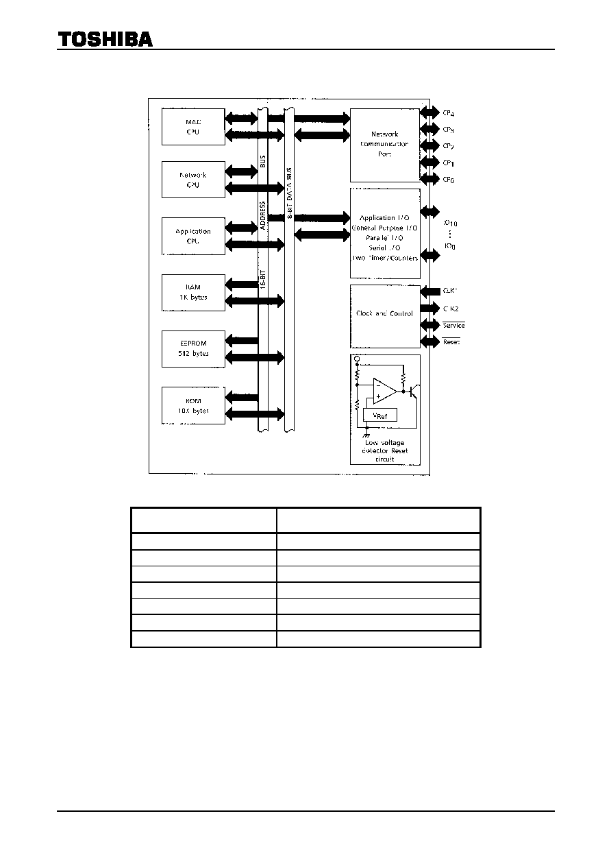
BLOCK DIAGRAM
ITEM
TMPN3120B1AM
CPU 8-bit
CPU◊3
RAM 1,024
bytes
ROM 10,240
bytes
EEPROM 512
bytes
16-bit Timer / Counter
2 channels
External Memory Interface
Not available
Package 32-pin
SOP
TMPN3120B1AM
2001-02-21 4/8
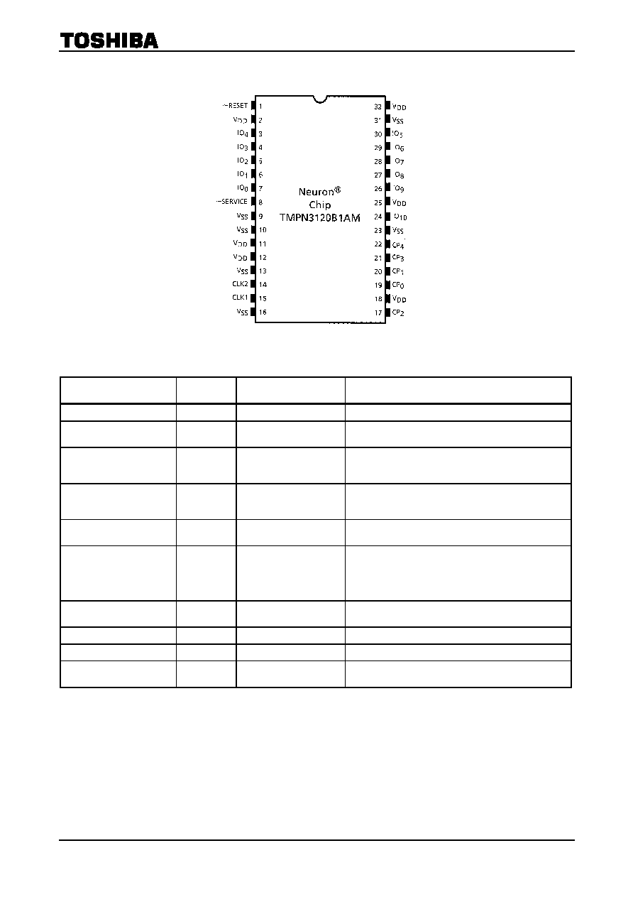
PIN ASSIGNMENT
PIN FUNCTION
PIN No.
PIN NAME
I / O
PIN FUNCTION
15
CLK1
Input
Oscillator connection, or external clock input.
14 CLK2
Output
Oscillator connection. Leave open when external clock is
input to CLK1.
1 ~RESET
I / O
(built-in configurable
pull-up)
Reset pin. (Active low)
8 ~SERVICE
I / O
(built-in configurable
pull-up)
Service pin. Indicator output during operation.
7~4 IO
0
~IO
3
I / O
Large current sink capacity (20mA).
General I / O port.
3, 30~28
IO
4
~IO
7
I / O
(built-in configurable
pull-up)
General I / O port. One of IO
4
to IO
7
can be specified as
No.1 timer / counter input. Output signal can be output to
IO
0
.
IO
4
can be used as the No.2 timer / counter input with
IO
1
as output.
27, 26, 24
IO
8
~IO
10
I / O
General I / O port. Can be used for serial communication
with other device.
2, 11, 12, 18, 25, 32
V
DD
Input
Power input (5.0V Typ.)
9, 10, 13, 16, 23, 31
V
SS
Input
Power input (0V GND)
19, 20, 17, 21, 22
CP
0
~CP
4
I / O
Bidirectional port for communications. Supports several
communications protocols by specifying mode.
* : The ~SERVICE and IO
4
to IO
7
terminals are programmable pull-ups.
All V
DD
terminals must be externally connected.
All V
SS
terminals must be externally connected.
TMPN3120B1AM
2001-02-21 5/8
MAXIMUM RATINGS
( V
SS
= 0V, V
SS
typ.)
CHARACTERISTICS SYMBOL RATING
UNIT
Power Supply Voltage
V
DD
-0.3~7.0 V
Input Voltage
V
IN
-0.3~V
DD
+0.3 V
Power Dissipation
PD
800
mW
Storage Temperature
T
stg
-65~150 ∞C
OPERATING CONDITIONS
ITEM SYMBOL
MIN
TYP.
MAX
UNIT
Operating Voltage
V
DD
4.5
5.0
5.5
V
V
IH
2.0
V
DD
V
Input Voltage ( TTL )
V
IL
V
SS
0.8 V
V
IH
V
DD
-
0.8
V
DD
V
Input Voltage ( CMOS )
V
IL
V
SS
0.8 V
Operating Frequency
f
osc
0.625
10 MHz
Operating Temperature
T
opr
-
40
85
∞C
ELECTRICAL CHARACTERISTICS
DC characteristic
( V
DD
= 5.0 V
±
10%, V
SS
= 0 V, Ta =
-
40~85∞C )
( Above operating conditions apply unless otherwise states. )
CHARACTERISTICS SYMBOL
PINS
TEST
CONDITION MIN
MAX
UNIT
I
OL
=20mA 0
0.8
V
LOW Output Voltage (1)
V
OL
(1)
IO
0
~IO
3
I
OL
=10mA 0
0.4
V
I
OL
=20mA 0 0.8
V
LOW Output Voltage (2)
V
OL
(2)
~SERVICE
Duty
cycle=50%
I
OL
=10mA 0 0.4
V
LOW Output Voltage (3)
V
OL
(3)
CP
2
, CP
3
I
OL
=40mA 0
1.0
V
LOW Output Voltage (4)
V
OL
(4)
Others (Note 1)
I
OL
=1.4mA 0
0.4
V
HIGH Output Voltage (1)
V
OH
(1)
IO
0
~IO
3
I
OH
=-1.4mA
V
DD
-0.4
V
DD
V
HIGH Output Voltage (2)
V
OH
(2)
~SERVICE
I
OH
=-1.4mA
V
DD
-0.4
V
DD
V
HIGH Output Voltage (3)
V
OH
(3)
CP
2
, CP
3
I
OH
=-40mA
V
DD
-1.0
V
DD
V
HIGH Output Voltage (4)
V
OH
(4)
Others (Note 1)
I
OH
=-1.4mA
V
DD
-0.4
V
DD
V
Input Current
I
IN
(Note 2)
V
IN
=V
SS
~V
DD
-10 +10 µA
Pull-up Current
I
PU
IO
4
~IO
7
~SERVICE,
~RESET (Note 3)
V
IN
=0V
-30
-300
µA
Low-voltage Detection Level
V
LVD
V
DD
3.8
4.5
V
Note1 : Output voltage characteristics exclude the ~RESET pin and CLK2 pin.
Note2 : Excludes pull-up input pins.
Note3 : The IO
4
to IO
7
and ~SERVICE pins have programmable pull-ups. ~RESET has a fixed pull-up.

TMPN3120B1AM
2001-02-21 6/8
ITEM SYMBOL
TYP.
MAX
UNIT
10 MHz
Clock 17
30
5 MHz
Clock 9
15
2.5 MHz Clock
6
8
1.25 MHz Clock
4
5
Operating
Mode
Current
Consumption
0.625 MHz Clock
I
DD (OP)
2 3
mA
Sleep Mode Current
Consumption
I
DD (SLP)
16 100 µA
Note:
Test conditions for current dissipation
V
DD
=5V, all output=with no load, all input=0.2V or below or V
DD
-0.2V, programmable pull-up=off, crystal
oscillator clock input, differential receiver disabled.
The current value ( typ. ) is a typical value when Ta=25∞C
The current value ( max ) applies to the rated temperature range at V
DD
=5.5V.
200µA ( typ. ) to 600µA ( max ) is added to the current of the differential receiver when the receiver is
enabled.
The differential receiver is enabled by either of the following conditions :
When the Neuron chip is in Run mode and the communication ports are in Differential mode.
When the Neuron chip is in Sleep mode, the communication ports are in Differential mode, and the
Comm Port Wakeup is not masked.

TMPN3120B1AM
2001-02-21 7/8
l Echelon, Neuron, LON, LonTalk, LonBuilder, NodeBuilder, L
ON
W
ORKS
, 3150, 3120 and LonManager are the
registered trade marks of America's Echelon Inc.
l The Neuron Chip is manufactured by Toshiba under license from Echelon Corporation, USA. A licensing
agreement between the customer and Echelon Corporation must be concluded before purchasing any of the
neuron chip products.
l The Neuron chip itself does not include the I
2
C object function. You need the "I
2
C Library" deliveried by
Echelon.
The Neuron chip and the I
2
C Library do not convey nor imply a right under any I
2
C patent rights of Philips
Electronics N.V. ( "Philips" ) to make, use or sell any product employing such patent rights. Please refer all
questions with respect to I
2
C patents and licenses to Philips at:
Mr. Gert-Jan Hessenlmann
Corporate Intellectual Property
Philips International B.V.
Prof. Holstlaan 6
Building WAH 1-100
P.O. Box 220
5600 AE, Eindhoven, The Netherlands
Phone : +31 40 274 32 61
Fax :
+31 40 274 34 89
E-mail : Gert.Jan.Hesselmann@philips.com.
TMPN3120B1AM
2001-02-21 8/8
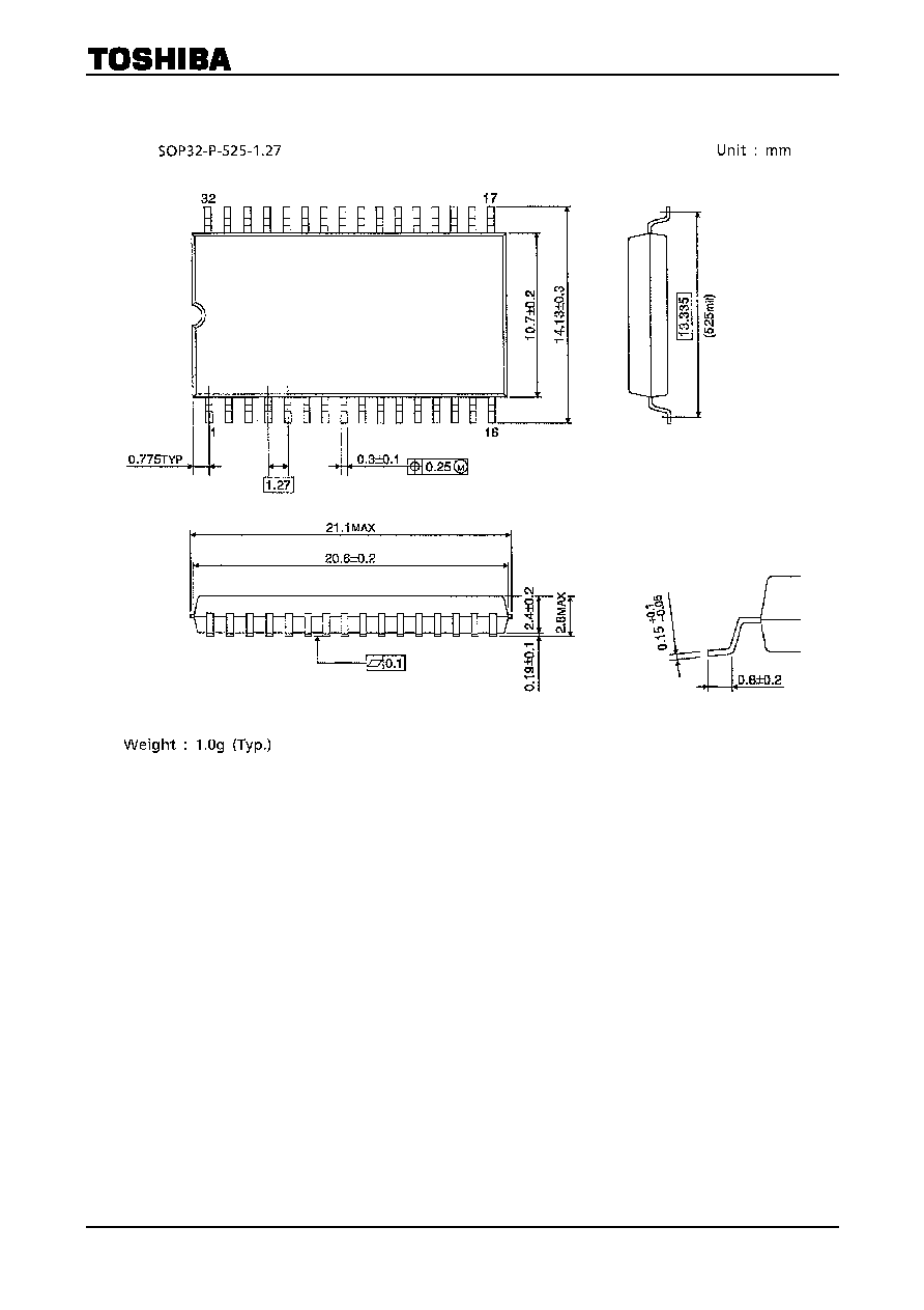
PACKCAGE DIMENSIONS