TPCA8014-H
2004-6-25
1
TOSHIBA Field Effect Transistor Silicon N Channel MOS Type (Ultra High speed U-MOSIII)
TPCA8014-H
High Speed and High Efficiency DC-DC Converters
Notebook PC Applications
Portable Equipment Applications
∑
Small footprint due to small and thin package
∑
High speed switching
∑
Small gate charge: Qsw = 7.4 nC (typ.)
∑
Low drain-source ON resistance: R
DS (ON)
= 10.5 mO (typ.)
∑
High forward transfer admittance: |Y
fs
| = TBD S (typ.)
∑
Low leakage current: I
DSS
= 10 µA (max) (V
DS
= 40 V)
∑
Enhancement mode: V
th
= 1.1 to 2.3 V (V
DS
= 10 V, I
D
= 1 mA)
Maximum Ratings
(Ta
=
25∞C)
Characteristics
Symbol
Rating
Unit
Drain-source voltage
V
DSS
40
V
Drain-gate voltage (R
GS
=
20 k
)
V
DGR
40
V
Gate-source voltage
V
GSS
±
20
V
DC
(Note 1)
I
D
30
Drain current
Pulsed (Note 1)
I
DP
90
A
Drain power dissipation (Tc=25
)
P
D
45
W
Drain power dissipation
(t
=
10 s)
(Note 2a)
P
D
2.8
W
Drain power dissipation
(t
=
10 s)
(Note 2b)
P
D
1.6
W
Single pulse avalanche energy
(Note 3)
E
AS
84
mJ
Avalanche current
I
AR
30
A
Repetitive avalanche energy
(Tc=25
) (Note 4)
E
AR
TBD
mJ
Channel temperature
T
ch
150
∞C
Storage temperature range
T
stg
-
55 to 150
∞C
Note: For (Note 1), (Note 2), (Note 3), (Note 4), please refer to the next
page.
This transistor is an electrostatic sensitive device. Please handle with caution.
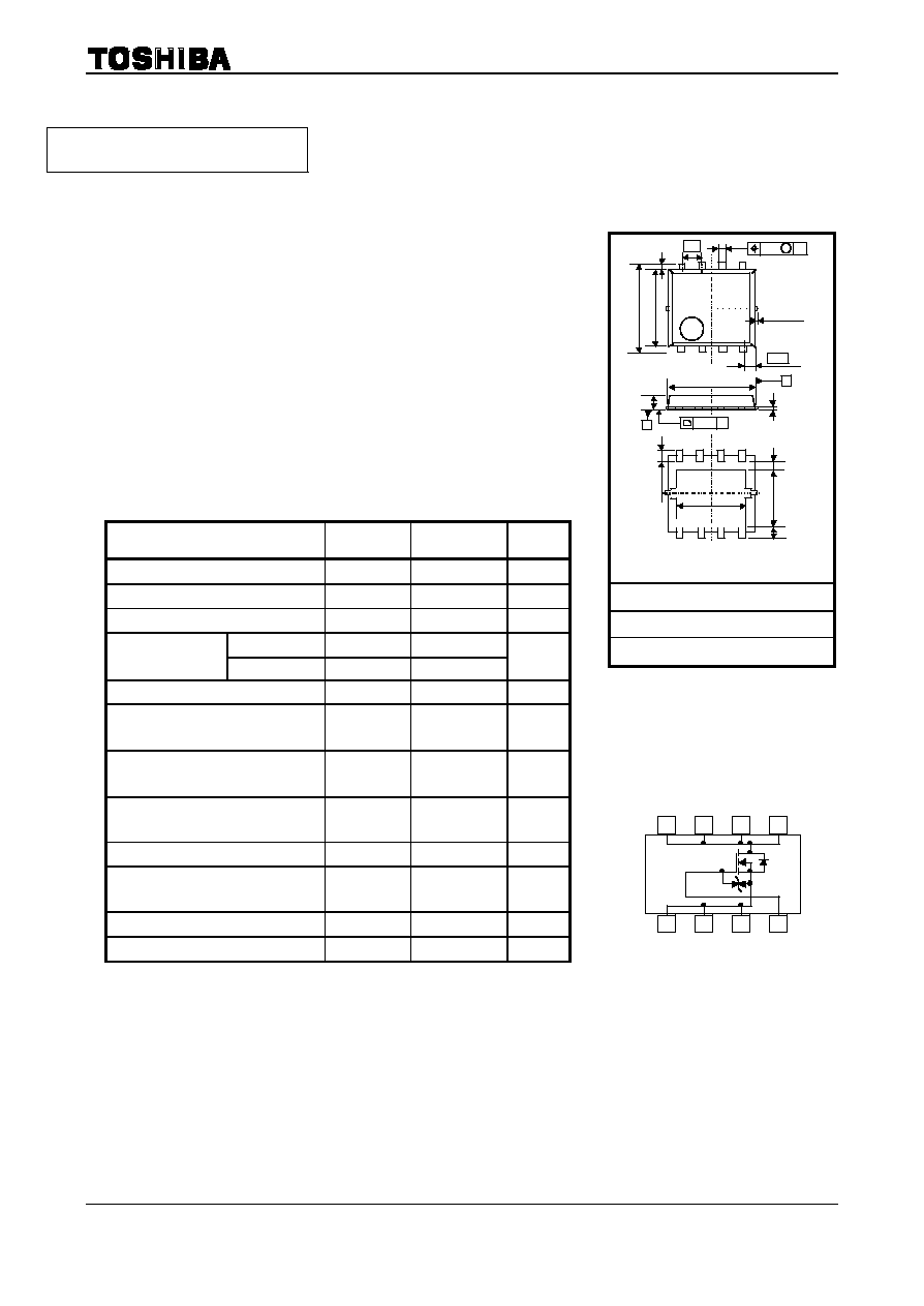
Unit: mm
0.5±0.1
6.0±0.3
1.27
0.4±0.1
5.0±0.2
0.595
0.05 M A
1
4
5
8
0.15±0.05
0.8±0.1
1.1±0.2
4.25±0.2
0.6±0.1
3.5±0.2
1
4
5
8
5.0±0.2
0.95±0.05
S
0.05 S
A
0.166±0.05
JEDEC
?
JEITA
?
TOSHIBA
2-5Q1A
Weight: 0.080 g (typ.)
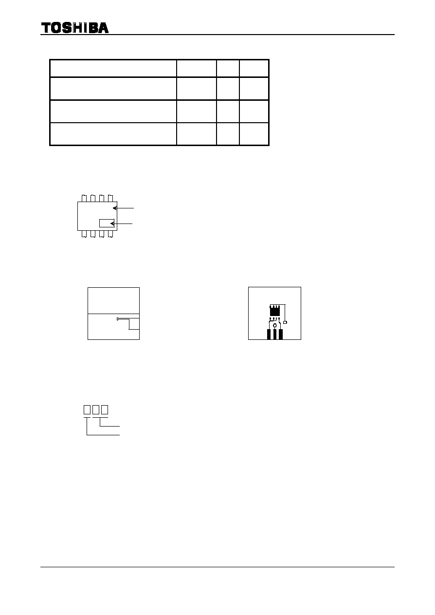
Circuit Configuration
8
6
1
2
3
7
5
4
1,2,3SOURCE 4GATE
5,6,7,8DRAIN
TENTATIVE
TPCA8014-H
2004-6-25
2
Thermal Characteristics
Characteristics
Symbol
Max
Unit
Thermal resistance, channel to case
(Tc=25
)
R
th (ch-c)
2.78
∞C/W
Thermal resistance, channel to ambient
(t
=
10 s)
(Note 2a)
R
th (ch-a)
44.6
∞C/W
Thermal resistance, channel to ambient
(t
=
10 s)
(Note 2b)
R
th (ch-a)
78.1
∞C/W
Marking
(Note 5)
Note 1: Please use devices on condition that the channel temperature is below 150∞C.
Note 2: (a) Device mounted on a glass-epoxy board (a)
(b) Device mounted on a glass-epoxy board (b)
Note 3: V
DD
=
24 V, T
ch
=
25∞C (initial), L
=
0.1 mH, R
G
=
25
,
I
AR
=
30 A
Note 4: Repetitive rating: pulse width limited by max channel temperature
Note 5:
(a)
FR-4
25.4
◊
25.4
◊
0.8
(Unit: mm)
(b)
FR-4
25.4
◊
25.4
◊
0.8
(Unit: mm)
*
Weekly code: (Three digits)
Week of manufacture
(01 for first week of year, continues up to 52 or 53)
Year of manufacture
(One low-order digits of calendar year)
Type
TPCA
8014-H
Lot No.
TPCA8014-H
2004-6-25
3
Electrical Characteristics
(Ta
=
25∞C)
Characteristics
Symbol
Test Condition
Min
Typ.
Max
Unit
Gate leakage current
I
GSS
V
GS
=
±
16 V, V
DS
=
0 V
±
10
µ
A
Drain cut-OFF current
I
DSS
V
DS
=
40 V, V
GS
=
0 V
10
µ
A
V
(BR) DSS
I
D
=
10 mA, V
GS
=
0 V
40
Drain-source breakdown voltage
V
(BR) DSX
I
D
=
10 mA, V
GS
=
-
20 V
25
V
Gate threshold voltage
V
th
V
DS
=
10 V, I
D
=
1 mA
1.1
2.3
V
V
GS
=
10 V , I
D
=
15 A
7.0
9.5
Drain-source ON resistance
R
DS (ON)
V
GS
=
4.5 V , I
D
=
15 A
10.5
15
m
Forward transfer admittance
|Y
f s
|
V
DS
=
10 V , I
D
=
15 A
TBD
TBD
S
Input capacitance
C
iss
1365
Reverse transfer capacitance
C
rss
110
Output capacitance
C
oss
500
pF
Gate resistance
R
g
V
DS
=
10 V , V
GS
=
0 V , f
=
1 MHz
1.0
Rise time
t
r
5
Turn-ON time
t
on
11
Fall time
t
f
3
Switching time
Turn-OFF time
t
off
Duty
<
=
1%, t
w
=
10
µ
s
18
ns
V
DD
-
32 V, V
GS
=
10 V , I
D
=
30 A
22
Total gate charge
(gate-source plus gate-drain)
Q
g
V
DD
-
32 V, V
GS
=
5 V , I
D
=
30 A
12
Gate-source charge 1
Q
gs1
5.1
Gate-drain ("miller") charge
Q
gd
4.9
Gate switch charge
Q
SW
V
DD
-
32 V, V
GS
=
10 V , I
D
=
30 A
7.4
nC
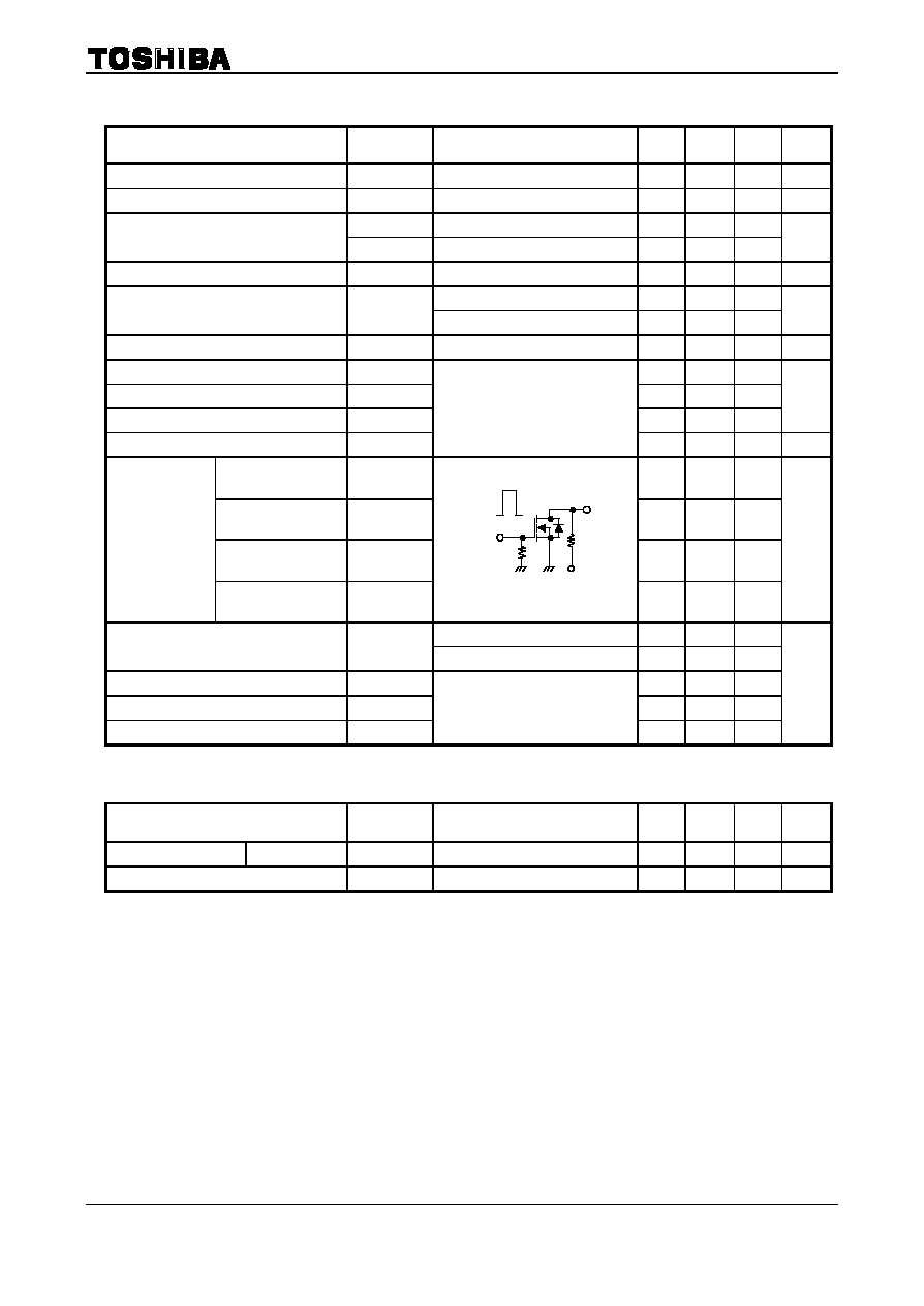
Source-Drain Ratings and Characteristics
(Ta
=
25∞C)
Characteristics
Symbol
Test Condition
Min
Typ.
Max
Unit
Drain reverse current
Pulse (Note 1)
I
DRP
90
A
Forward voltage (diode)
V
DSF
I
DR
=
30 A, V
GS
=
0 V
-
1.2
V
R
L
=
1.33
V
DD
-
20 V
0 V
V
GS
10 V
4.7
I
D
=
15 A
V
OUT
TPCA8014-H
2004-6-25
4
∑
The information contained herein is subject to change without notice.
∑
The information contained herein is presented only as a guide for the applications of our products. No
responsibility is assumed by TOSHIBA for any infringements of patents or other rights of the third parties which
may result from its use. No license is granted by implication or otherwise under any patent or patent rights of
TOSHIBA or others.
∑
TOSHIBA is continually working to improve the quality and reliability of its products. Nevertheless, semiconductor
devices in general can malfunction or fail due to their inherent electrical sensitivity and vulnerability to physical
stress. It is the responsibility of the buyer, when utilizing TOSHIBA products, to comply with the standards of
safety in making a safe design for the entire system , and to avoid situations in which a malfunction or failure of
such TOSHIBA products could cause loss of human life, bodily injury or damage to property.
In developing your designs, please ensure that TOSHIBA products are used within specified operating ranges as
set forth in the most recent TOSHIBA products specifications. Also, please keep in mind the precautions and
conditions set forth in the "Handling Guide for Semiconductor Devices," or "TOSHIBA Semiconductor Reliability
Handbook" etc..
∑
The TOSHIBA products listed in this document are intended for usage in general electronics applications
(computer, personal equipment, office equipment, measuring equipment, industrial robotics, domestic appliances,
etc.). These TOSHIBA products are neither intended nor warranted for usage in equipment that requires
extraordinarily high quality and/or reliability or a malfunction or failure of which may cause loss of human life or
bodily injury ("Unintended Usage"). Unintended Usage include atomic energy control instruments, airplane or
spaceship instruments, transportation instruments, traffic signal instruments, combustion control instruments,
medical instruments, all types of safety devices, etc.. Unintended Usage of TOSHIBA products listed in this
document shall be made at the customer's own risk.
∑
TOSHIBA products should not be embedded to the downstream products which are prohibited to be produced
and sold, under any law and regulations.
030619EAA
RESTRICTIONS ON PRODUCT USE