 | –≠–ª–µ–∫—Ç—Ä–æ–Ω–Ω—ã–π –∫–æ–º–ø–æ–Ω–µ–Ω—Ç: TK2019 | –°–∫–∞—á–∞—Ç—å:  PDF PDF  ZIP ZIP |

T r i p a t h T e c h n o l o g y, I n c . - T e c h n i c a l I n f o r m a t i o n
1
TK2019 ≠ MC/2.1/10-03
TK2019
STEREO 20W (4
) CLASS-TTM DIGITAL AUDIO AMPLIFIER
DRIVER USING DIGITAL POWER PROCESSING (DPPTM)
TECHNOLOGY
P r e l i m i n a r y I n f o r m a t i o n R e v i s i o n 2 . 1 ≠ O c t o b e r 2 0 0 3
G E N E R A L D E S C R I P T I O N
T h e T K 2 0 1 9 ( T C 2 0 0 1 / T P S 1 0 3 5 c h i p s e t ) i s a s t e r e o s i n g l e e n d e d 2 0 W
c o n t i n u o u s a v e r a g e p o w e r p e r c h a n n e l , C l a s s - T D i g i t a l A u d i o P o w e r
A m p l i f i e r u s i n g T r i p a t h ' s p r o p r i e t a r y D i g i t a l P o w e r P r o c e s s i n g
T M
t e c h n o l o g y .
T h e T K 2 0 1 9 c h i p s e t c o n s i s t s o f 1 T C 2 0 0 1 a n d 2 T P S 1 0 3 5 ' s t o o b t a i n a
s i n g l e e n d e d s t e r e o c o n f i g u r a t i o n . C l a s s - T a m p l i f i e r s o f f e r b o t h t h e a u d i o
f i d e l i t y o f C l a s s - A B a n d t h e p o w e r e f f i c i e n c y o f C l a s s - D a m p l i f i e r s .
A P P L I C A T I O N S
5.1-Channel powered DVD player
Mini/Micro Component Systems
Home Theater
Stereo applications (4 / 8)
B E N E F I T S
Single Supply Operation
Very High Efficiency
Wide Dynamic Range
Compact layout
F E A T U R E S
Class-T Architecture
High Output power
20W @ 4
, 10% THD+N Single Ended
11W @ 8
, 10% THD+N Single Ended
Audiophile Quality Sound
0.03% THD+N @ 11W 4
Single Ended
0.03% THD+N @ 6W 8
Single Ended
High Efficiency
92% @ 20W 4 Single Ended
93% @ 11W 8 Single Ended
Dynamic Range >100 dB

T r i p a t h T e c h n o l o g y, I n c . - T e c h n i c a l I n f o r m a t i o n
2
TK2019 ≠ MC/2.1/10-03
A B S O L U T E M A X I M U M R A T I N G S ≠ T C 2 0 0 1
(Note 1)
SYMBOL PARAMETER
Value
UNITS
V
5
5V Power Supply
6
V
Vlogic Input
Logic
Level
V
5
+0.3V V
TA
Operating Free-air Temperature Range
-40 to 85
∞C
T
STORE
Storage Temperature Range
-55 to 150
∞C
T
JMAX
Maximum Junction Temperature
150
∞C
ESD
HB
ESD Susceptibility ≠ Human Body Model (Note 2), all pins
2000
V
Note 1: Absolute Maximum Ratings indicate limits beyond which damage to the device may occur.
See the table below for Operating Conditions.
Note 2: Human body model, 100pF discharged through a 1.5K
resistor.
A B S O L U T E M A X I M U M R A T I N G S ≠ T P S 1 0 3 5
(Note 1)
SYMBOL PARAMETER
Value
UNITS
V
CC
Power Supply
26
V
Vlogic Input
Logic
Level
5.5
V
T
A
Operating Free-air Temperature Range
-40 to 85
∞C
T
STORE
Storage Temperature Range
-40 to 150
∞C
T
JMAX
Maximum Junction Temperature
150
∞C
ESD
HB
ESD Susceptibility ≠ Human Body Model (Note 2), all pins except 1, 8
Pins 1, 8
2000
400
V
ESD
MM
ESD Susceptibility ≠ Machine model (Note 3), all pins
200
V
Note 3: Machine model, 220pF ≠ 240pF discharged through all pins.
O P E R A T I N G C O N D I T I O N S ≠ T C 2 0 0 1
SYMBOL PARAMETER MIN.
TYP.
MAX.
UNITS
V5
Supply Voltage
4.5
5
5.5
V
V
HI
Logic Input High
V5-1.0
V
V
LO
Logic Input Low
1
V
T
A
Operating Temperature Range
-40
25
85
∞C
O P E R A T I N G C O N D I T I O N S ≠ T P S 1 0 3 5
SYMBOL PARAMETER MIN.
TYP.
MAX.
UNITS
V
CC
Power Supply
8
25
V
V
HI
Logic Input High
TBD
V
V
LO
Logic Input Low
TBD
V
T
A
Operating Temperature Range
-40
25
85
∞C
T H E R M A L C H A R A C T E R I S T I C S
TC2001
SYMBOL PARAMETER
Value
UNITS
JA
Junction-to-ambient Thermal Resistance (still air)
80
∞C/W

T r i p a t h T e c h n o l o g y, I n c . - T e c h n i c a l I n f o r m a t i o n
3
TK2019 ≠ MC/2.1/10-03
TPS1035
SYMBOL PARAMETER
Value
UNITS
JA
Junction-to-Ambient Thermal Resistance
50
∞C/W
JC
Junction-to-case Thermal Resistance
8
∞C/W
E L E C T R I C A L C H A R A C T E R I S T I C S ≠ T C 2 0 0 1
SYMBOL PARAMETER MIN.
TYP.
MAX.
UNITS
I5
Supply Current
60
mA
fsw
Switching Frequency (adjustable via CFB)
600
650
kHz
V
IN
Input
Sensitivity
0
1.5
V
V
OUTHI
High Output Voltage
V5-0.5
V
V
OUTLO
Low Output Voltage
100
mV
R
IN
Input
Impedance
2
k
Input
DC
Bias
2.5
V
E L E C T R I C A L C H A R A C T E R I S T I C S ≠ T K 2 0 1 9
T
A
= 25
∞C. See Application/Test Circuit. Unless otherwise noted, the supply voltage is V
DD
= 24V.
SYMBOL PARAMETER
CONDITIONS MIN.
TYP.
MAX.
UNITS
I
q
Quiescent Current
(No load, Mute = 0V)
V
DD
= 24V
V5 = 5V
20
27
60
mA
mA
I
MUTE
Mute Supply Current
(No load, TC2001 Mute = 5V,
TPS1035 Sleep = 5V)
V
DD
= 24V
V5 = 5V
2
7
µA
mA
V
IH
High-level input voltage (MUTE)
I
IH
= See Mute Control Section
3.5
V
V
IL
Low-level input voltage (MUTE)
I
IL
= See Mute Control Section
1.0
V
I
SC
Short circuit current limit
V
DD
= 24V, T=25
o
C
7.5
A
I
VPPSENSE
VPPSENSE Threshold Currents
Over-voltage turn on (muted)
Over-voltage turn off (mute off)
Under-voltage turn off (mute off)
Under-voltage turn on (muted)
138
62
162
154
79
72
178
87
µA
µA
µA
µA
V
VPPSENSE
Threshold Voltages with
R
VPPSENSE
= 187K
(Note 4, Note 5)
Over-voltage turn on (muted)
Over-voltage turn off (mute off)
Under-voltage turn off (mute off)
Under-voltage turn on (muted)
25.8
11.6
30.3
28.8
14.8
13.5
33.3
16.3
V
V
V
V
Note 4: These supply voltages are calculated using the IVPPSENSE values shown in the Electrical Characteristics
table. The typical voltage values shown are calculated using a RVPPSENSE value of 187kohm without any
tolerance variation. The minimum and maximum voltage limits shown include either a +1% or ≠1% (+1% for
Over-voltage turn on and Under-voltage turn off, -1% for Over-voltage turn off and Under-voltage turn on)
variation of RVPPSENSE off the nominal value. These voltage specifications are examples to show both
typical and worst case voltage ranges for a given RVPPSENSE resistor values of 187kohm. Please refer to
the Application Information section for a more detailed description of how to calculate the over and under
voltage trip voltages for a given resistor value.
Note 5: The fact that the over-voltage turn on specifications exceed the absolute maximum of 26V for the TK2019
does not imply that the part will work at these elevated supply voltages. It also does not imply that the
TK2019 is tested or guaranteed at these supply voltages. The supply voltages are simply a calculation based
on the process spread of the IVPPSENSE currents (see note 7). The supply voltage must be maintained
below the absolute maximum of 26V or permanent damage to the TK2019 may occur.

T r i p a t h T e c h n o l o g y, I n c . - T e c h n i c a l I n f o r m a t i o n
4
TK2019 ≠ MC/2.1/10-03
P E R F O R M A N C E C H A R A C T E R I S T I C S ≠ T K 2 0 1 9
T
A
= 25
∞C. Unless otherwise noted, V
DD
= 24V, f=1kHz, and the measurement bandwidth is 20kHz.
SYMBOL PARAMETER
CONDITIONS MIN.
TYP.
MAX.
UNITS
P
OUT
Output Power
(Continuous Average/Channel)
(Note 13)
V
DD
= 24V, R
L
= 8
THD+N = 0.03%
THD+N = 1.0%
THD+N = 10.0%
V
DD
= 24V, R
L
= 4
THD+N = 0.03%
THD+N = 1.0%
THD+N = 10.0%
6
8
11
11
15
20
W
W
W
W
W
W
THD + N Total Harmonic Distortion Plus
Noise
P
OUT
= 5W/Channel, R
L
= 8
V
CC
= 24V
P
OUT
= 10W/Channel, R
L
= 4
V
CC
= 24V
0.025
0.025
%
%
IHF-IM IHF
Intermodulation
Distortion 19kHz, 20kHz, 1:1 (IHF), R
L
= 4
P
OUT
= 2.5W/Channel
0.01 %
SNR Signal-to-Noise
Ratio
A-Weighted
0dB = 10W/Channel, R
L
= 8
102
dB
CS Channel
Separation
0dB = 6.5W, R
L
= 4
, f=1kHz
72 dB
A
V
Amplifier
Gain
P
OUT
= 5W/Channel, R
L
= 8
,
See Application / Test Circuit
10 V/V
A
VERROR
Channel to Channel Gain Error
P
OUT
= 5W/Channel, R
L
= 8
See Application / Test Circuit
0.5
dB
Power Efficiency
P
OUT
= 11W/Channel, R
L
= 8
P
OUT
= 20W/Channel, R
L
= 4
93
92
%
%
e
N
Output Noise Voltage
A-Weighted, input AC grounded,
R
FBC
= 9.1k
, R
FBB
= 1k
75
µV
T r i p a t h T e c h n o l o g y, I n c . - T e c h n i c a l I n f o r m a t i o n
5
TK2019 ≠ MC/2.1/10-03
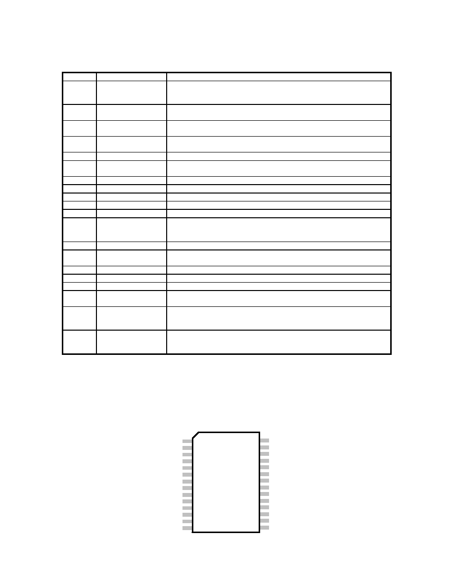
T C 2 0 0 1 A U D I O S I G N A L P R O C E S S O R P I N D E S C R I P T I O N S
Pin
Function
Description
1
BIASCAP
Bandgap reference times two (typically 2.5VDC). Used to set the
common mode voltage for the input op amps. This pin is not capable of
driving external circuitry
.
2, 6
FBKGND2,
FBKGND1
Ground Kelvin feedback (Channels 1 & 2)
3
DCMP
Internal mode selection. This pin must be grounded for proper device
operation.
4, 7
FBKOUT2,
FBKOUT1
Switching feedback (Channels 1 & 2)
5
VPWR
Test pin. Must be left floating.
8
HMUTE
Logic output. A logic high indicates both amplifiers are muted, due to the
mute pin state, or a "fault".
9, 12
Y1, Y2
Non-inverted switching modulator outputs.
10, 11
Y1B, Y2B
Inverted switching modulator outputs.
13 NC
No
connect
14, 16
OCD2, OCD1
Over Current Detect pins. These pins should be tied to ground.
15
REF
Internal bandgap reference voltage; approximately 1.2 VDC.
17
VNNSENSE
Negative supply voltage sense input. This pin is used for both over and
under voltage sensing for the VNN supply. Not used on the TK2019.
Connect this pin to AGND through a 10k
resistor.
18
OVRLDB
A logic low output indicates the input signal has overloaded the amplifier.
19
VPPSENSE
Positive supply voltage sense input. This pin is used for both over and
under voltage sensing for the VPP supply.
20 AGND
Analog
Ground.
21
V5
5 Volt power supply input.
22, 27
OAOUT1, OAOUT2
Input stage output pins.
23, 28
INV1, INV2
Single-ended inputs. Inputs are a "virtual" ground of an inverting opamp
with approximately 2.4VDC bias.
24
MUTE
When set to logic high, both amplifiers are muted and in idle mode.
When low (grounded), both amplifiers are fully operational. If left floating,
the device stays in the mute mode. Ground if not used.
25, 26
BBM1, BBM0
Break-before-make timing control to prevent shoot-through in the output
MOSFETs. When using with the TPS1035, these pins should both be
set to 5V.
T C 2 0 0 1 A U D I O S I G N A L P R O C E S S O R P I N O U T
REF
VNNSENSE
VPPSENSE
AGND
OAOUT1
MUTE
BBM1
BBM0
OAOUT2
INV2
FBKGND2
OCD2
Y2
Y2B
Y1B
Y1
HMUTE
FBKOUT1
FBKGND1
VPW R
FBKOUT2
DCMP
1
15
14
13
11
10
12
9
8
7
6
5
4
3
2
28-pin SOIC
(Top View)
16
17
18
BIASCAP
INV1
V5
OVRLDB
OCD1
NC
21
20
19
22
23
24
25
26
27
28